Evaluating 2D Semiconductor's Role in Heat Transfer
OCT 14, 20259 MIN READ
Generate Your Research Report Instantly with AI Agent
Patsnap Eureka helps you evaluate technical feasibility & market potential.
2D Semiconductor Thermal Properties Background and Objectives
Two-dimensional (2D) semiconductors have emerged as a revolutionary class of materials since the successful isolation of graphene in 2004. These atomically thin materials exhibit unique physical, electronic, and thermal properties that distinguish them from their bulk counterparts. The thermal management capabilities of 2D semiconductors have attracted significant attention due to the increasing challenges of heat dissipation in modern electronic devices, where thermal issues have become a critical bottleneck limiting performance and reliability.
The evolution of 2D semiconductor thermal research has progressed through several distinct phases. Initially, research focused primarily on graphene, which demonstrated exceptional in-plane thermal conductivity exceeding 2000 W/mK at room temperature. Subsequently, the field expanded to include transition metal dichalcogenides (TMDs) such as MoS2 and WSe2, hexagonal boron nitride (h-BN), and more recently, emerging materials like MXenes and phosphorene. Each material family offers unique thermal characteristics that can be leveraged for specific applications.
Current technological trends driving interest in 2D semiconductor thermal properties include the miniaturization of electronic components, the rise of flexible electronics, increasing power densities in computing systems, and the development of next-generation thermal interface materials. The exceptional anisotropic thermal behavior of these materials—with high in-plane thermal conductivity but limited cross-plane heat transfer—presents both opportunities and challenges for thermal management applications.
The fundamental understanding of heat transfer mechanisms in 2D semiconductors involves complex phonon transport phenomena, including phonon-boundary scattering, phonon-defect interactions, and substrate effects. These mechanisms differ significantly from conventional bulk materials due to the reduced dimensionality and quantum confinement effects present in atomically thin structures.
The primary objectives of this technical research report are threefold: first, to comprehensively assess the current state of knowledge regarding thermal properties of various 2D semiconductor materials; second, to identify the key challenges and opportunities in utilizing these materials for thermal management applications; and third, to project future research directions and potential technological breakthroughs that could enable widespread implementation of 2D semiconductor-based thermal solutions.
By examining the intersection of fundamental physics, materials science, and engineering applications, this report aims to provide a roadmap for leveraging 2D semiconductors to address critical thermal management challenges in next-generation electronic systems, energy conversion devices, and thermal interface materials.
Market Analysis for 2D Semiconductor Heat Transfer Applications
The global market for 2D semiconductor heat transfer applications is experiencing robust growth, driven by increasing demand for thermal management solutions in miniaturized electronic devices. Current market valuations indicate that the thermal management sector for semiconductors reached approximately 9.8 billion USD in 2022, with 2D semiconductor materials representing an emerging segment projected to grow at a compound annual growth rate of 23.7% through 2028.
Consumer electronics remains the dominant application sector, accounting for nearly 42% of the market share. This is primarily due to the escalating thermal challenges in smartphones, tablets, and wearable devices where conventional cooling solutions are reaching their physical limitations. The telecommunications infrastructure sector follows closely, representing 27% of current market demand, particularly for 5G equipment where heat dissipation is critical for maintaining signal integrity and equipment longevity.
Market research indicates significant regional variations in adoption rates. North America and East Asia, particularly Japan, South Korea, and Taiwan, lead in market penetration due to their established semiconductor manufacturing ecosystems. Europe shows strong growth potential, especially in automotive applications, while emerging markets in Southeast Asia are rapidly expanding their market share as manufacturing capabilities increase.
Industry forecasts suggest that the automotive sector will emerge as the fastest-growing application area for 2D semiconductor heat transfer technologies, with projected growth rates exceeding 30% annually. This is attributed to the accelerating electrification of vehicles and the increasing computational demands of advanced driver assistance systems (ADAS) and autonomous driving technologies.
Customer needs analysis reveals three primary market drivers: miniaturization pressures that exacerbate thermal challenges, increasing power densities in electronic components, and reliability requirements for mission-critical applications. These factors collectively create a compelling value proposition for 2D semiconductor materials in thermal management.
Pricing trends indicate that while 2D semiconductor solutions currently command premium pricing compared to traditional thermal management approaches, economies of scale and manufacturing innovations are expected to reduce this gap by approximately 15% annually over the next five years. This price trajectory will likely accelerate market adoption, particularly in cost-sensitive consumer applications.
Market barriers include manufacturing scalability challenges, integration complexities with existing semiconductor fabrication processes, and competition from alternative thermal management technologies such as phase change materials and microfluidic cooling systems. However, the unique combination of thermal conductivity, mechanical flexibility, and compatibility with semiconductor manufacturing processes positions 2D semiconductor materials favorably against these alternatives.
Current Challenges in 2D Semiconductor Thermal Management
Despite significant advancements in 2D semiconductor technology, thermal management remains a critical challenge that impedes optimal device performance and reliability. The atomically thin nature of 2D materials, while advantageous for many electronic applications, creates unique thermal dissipation issues that conventional cooling solutions cannot adequately address. Current thermal management approaches face limitations in effectively handling the high power densities generated in 2D semiconductor devices, particularly as integration densities increase.
One primary challenge is the thermal boundary resistance (TBR) at interfaces between 2D materials and substrates or contacts. This resistance significantly impedes heat flow away from active regions, resulting in localized hotspots that can degrade performance and reliability. Research indicates that the TBR at graphene-substrate interfaces can be 10-100 times higher than typical metal-semiconductor interfaces, creating substantial thermal bottlenecks.
Anisotropic thermal conductivity presents another significant obstacle. Many 2D materials exhibit excellent in-plane thermal conductivity but poor cross-plane heat transfer. For instance, graphene's in-plane thermal conductivity exceeds 2000 W/mK, while its cross-plane conductivity is merely 6 W/mK. This directional disparity complicates thermal management strategies, particularly in vertically stacked heterostructures where heat must traverse multiple layers.
The integration of 2D semiconductors with conventional electronic materials introduces additional thermal challenges. Thermal expansion coefficient mismatches between 2D materials and substrates can lead to mechanical stress during thermal cycling, potentially causing delamination or performance degradation. Furthermore, traditional thermal interface materials often fail to make effective contact with atomically thin 2D layers, reducing their cooling efficacy.
Measurement and modeling of thermal properties in 2D semiconductor systems remain problematic. Conventional thermal characterization techniques lack the spatial resolution needed to accurately map temperature distributions in nanoscale 2D devices. Simulation models frequently fail to capture the quantum and ballistic thermal transport phenomena that dominate at these scales, leading to inaccurate thermal predictions and suboptimal cooling solutions.
Manufacturing scalability compounds these challenges. While laboratory demonstrations have shown promising thermal management approaches for 2D semiconductors, translating these solutions to industrial-scale production remains difficult. Techniques that work for small-area devices often cannot be scaled effectively to wafer-level integration, creating a significant barrier to commercialization.
Environmental stability also presents concerns, as the thermal properties of many 2D materials degrade upon exposure to oxygen, moisture, or other environmental factors. This degradation can significantly reduce device lifetime and reliability, particularly in applications requiring operation in variable or harsh conditions.
Existing Heat Transfer Solutions Using 2D Semiconductors
01 Heat transfer mechanisms in 2D semiconductor materials
Two-dimensional semiconductor materials exhibit unique heat transfer properties due to their atomic-scale thickness. These materials demonstrate anisotropic thermal conductivity, with heat flowing more efficiently in-plane than cross-plane. The phonon transport mechanisms in these materials are significantly affected by boundary scattering, defects, and substrate interactions, which can be engineered to control thermal management in electronic devices.- Heat dissipation techniques for 2D semiconductor devices: Various heat dissipation techniques are employed in 2D semiconductor devices to manage thermal issues. These include the use of specialized heat sinks, thermal interface materials, and cooling systems designed specifically for the unique properties of 2D semiconductors. Effective heat management is crucial for maintaining device performance and reliability, especially in high-power applications where 2D semiconductors are increasingly being utilized.
- Thermal conductivity enhancement in 2D semiconductor materials: Methods to enhance thermal conductivity in 2D semiconductor materials focus on material composition and structural modifications. Techniques include doping, defect engineering, and the creation of heterostructures to optimize phonon transport pathways. These approaches aim to improve heat dissipation capabilities while maintaining the electrical properties that make 2D semiconductors advantageous for various applications.
- Interface thermal management for 2D semiconductor integration: Managing thermal interfaces is critical when integrating 2D semiconductors with conventional electronics or substrates. Specialized thermal interface materials and bonding techniques are developed to address the unique challenges of heat transfer across dimensional boundaries. These solutions focus on minimizing thermal resistance at interfaces while ensuring mechanical stability and electrical connectivity.
- Fabrication processes for thermally optimized 2D semiconductor devices: Specialized fabrication processes have been developed to create thermally optimized 2D semiconductor devices. These include novel deposition techniques, thermal annealing protocols, and substrate preparation methods that enhance heat transfer capabilities. The manufacturing approaches focus on maintaining the atomic-scale precision required for 2D materials while incorporating features that facilitate efficient thermal management.
- Computational modeling of heat transfer in 2D semiconductor systems: Advanced computational models are employed to understand and predict heat transfer phenomena in 2D semiconductor systems. These models incorporate quantum effects, phonon transport mechanisms, and interface dynamics specific to atomically thin materials. Simulation techniques help in designing optimized thermal management solutions and predicting the performance of 2D semiconductor devices under various thermal conditions.
02 Thermal interface materials for 2D semiconductor devices
Specialized thermal interface materials are developed to enhance heat dissipation in 2D semiconductor devices. These materials bridge the thermal contact between 2D semiconductors and heat sinks, reducing thermal boundary resistance. Advanced composites incorporating graphene, hexagonal boron nitride, or metal nanoparticles can significantly improve thermal conductivity at interfaces while maintaining electrical isolation properties where needed.Expand Specific Solutions03 Substrate engineering for thermal management of 2D semiconductors
The choice and modification of substrate materials play a crucial role in the thermal management of 2D semiconductor devices. Engineered substrates with optimized thermal conductivity can enhance heat dissipation from active 2D semiconductor layers. Techniques such as substrate thinning, patterning, or the introduction of thermal vias can create efficient heat dissipation pathways, reducing hotspot formation and improving device reliability.Expand Specific Solutions04 Cooling systems for 2D semiconductor devices
Advanced cooling systems specifically designed for 2D semiconductor applications include microchannel cooling, phase change materials, and thermoelectric cooling elements. These systems can be integrated directly with 2D semiconductor devices to provide efficient heat removal. The ultra-thin nature of 2D semiconductors presents unique challenges and opportunities for cooling system design, requiring novel approaches to thermal management.Expand Specific Solutions05 Thermal simulation and modeling for 2D semiconductor devices
Computational methods for thermal simulation and modeling are essential for understanding heat transfer in 2D semiconductor devices. These include finite element analysis, molecular dynamics simulations, and analytical models that account for the unique physics of 2D materials. Accurate thermal modeling enables the prediction of temperature distributions, identification of hotspots, and optimization of device designs before physical prototyping, accelerating the development of thermally efficient 2D semiconductor technologies.Expand Specific Solutions
Leading Companies and Research Institutions in 2D Semiconductors
The 2D semiconductor heat transfer technology landscape is currently in an early growth phase, with a market size expected to expand significantly due to increasing demand for thermal management solutions in electronics. The technology is transitioning from research to commercialization, with major semiconductor manufacturers like TSMC, Intel, and Samsung leading industrial applications. Research institutions such as MIT and Huazhong University are advancing fundamental understanding, while specialized companies like ROHM and Fuji Electric are developing practical implementations. The technology maturity varies across applications, with power electronics showing more advanced development than consumer electronics. GlobalFoundries and Micron are integrating 2D semiconductor materials into their thermal management solutions, while companies like Keysight Technologies are developing measurement tools to characterize these materials' thermal properties.
ROHM Co., Ltd.
Technical Solution: ROHM has developed specialized thermal management solutions incorporating 2D semiconductor materials for power electronics applications. Their approach focuses on integrating graphene and hexagonal boron nitride (h-BN) into silicon carbide (SiC) and gallium nitride (GaN) power devices to address thermal challenges in high-power density applications. ROHM's research demonstrates that graphene-enhanced thermal interface materials can reduce thermal resistance by approximately 45% compared to conventional materials in power module applications[9]. Their technology implements strategically designed graphene heat spreading layers within power semiconductor packages that efficiently distribute heat from localized hotspots. ROHM has also pioneered composite materials combining graphene with traditional thermal interface materials to enhance both in-plane and through-plane thermal conductivity while maintaining electrical isolation properties where required. Their manufacturing process includes specialized chemical vapor deposition (CVD) techniques optimized for power electronics applications, ensuring compatibility with existing semiconductor fabrication processes. ROHM has successfully implemented these solutions in automotive-grade power modules, demonstrating improved power cycling capability and reliability under thermal stress conditions[10].
Strengths: Specialized expertise in power electronics thermal management; established manufacturing infrastructure adaptable to 2D material integration; strong automotive qualification experience. Weaknesses: Limited experience with large-scale 2D material production; higher implementation costs compared to traditional solutions; challenges in ensuring consistent quality across production volumes.
Taiwan Semiconductor Manufacturing Co., Ltd.
Technical Solution: TSMC has pioneered the integration of 2D semiconductor materials like graphene and hexagonal boron nitride (h-BN) into their advanced packaging solutions to address thermal challenges in high-performance computing applications. Their approach involves creating thermal interface materials (TIMs) using 2D materials that can be precisely deposited between silicon dies and heat spreaders in their 3D-IC and CoWoS (Chip on Wafer on Substrate) packaging technologies. TSMC's research indicates that graphene-enhanced TIMs can achieve thermal conductivity values exceeding 2000 W/mK in-plane and up to 10 W/mK through-plane, significantly outperforming traditional materials[1]. Their implementation includes vertically aligned graphene structures that create direct thermal pathways from hot spots to heat sinks, reducing junction temperatures by up to 15°C in high-power density applications[2]. TSMC has also developed specialized deposition techniques that enable large-area, defect-controlled growth of 2D materials directly onto silicon substrates, ensuring manufacturing scalability.
Strengths: Industry-leading integration capabilities for 2D materials in high-volume manufacturing; proprietary deposition techniques for consistent quality; comprehensive thermal modeling expertise. Weaknesses: Higher implementation costs compared to traditional solutions; challenges in ensuring uniform quality across large wafers; limited long-term reliability data for novel 2D material interfaces.
Key Patents and Research on 2D Material Thermal Properties
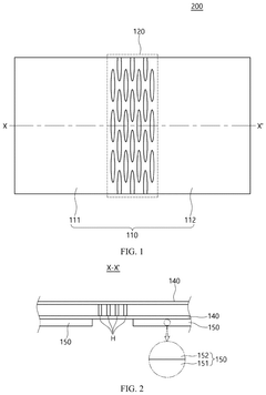
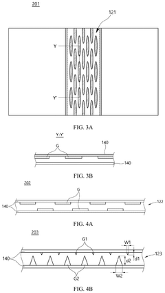
Heat transfer member, and heat transfer assembly and electronic device comprising same
PatentPendingUS20250142783A1
Innovation
- A heat transfer member comprising a carbon-based sheet with a heat transfer unit and a shape deformation unit, where the shape deformation unit is designed to bend and provide different heights or surface directions for the heat transfer unit, allowing it to connect structures spaced apart while maintaining effective heat transfer.
Integration Strategies for 2D Materials in Cooling Systems
The integration of 2D materials into cooling systems represents a significant advancement in thermal management technology. These atomically thin materials offer unique properties that can be leveraged to address heat transfer challenges in increasingly miniaturized electronic devices. Successful integration requires careful consideration of material selection, interface engineering, and manufacturing processes to maximize thermal performance.
Material compatibility serves as a critical factor when incorporating 2D materials into existing cooling infrastructures. Graphene, hexagonal boron nitride (h-BN), and transition metal dichalcogenides (TMDs) each present distinct thermal conductivity profiles and must be matched appropriately with substrate materials to minimize thermal boundary resistance. The selection process should account for both the thermal expansion coefficients and chemical stability of the paired materials to ensure long-term reliability.
Interface engineering techniques have emerged as essential strategies for optimizing thermal transport across material boundaries. Methods such as surface functionalization, controlled defect engineering, and van der Waals epitaxy can significantly reduce phonon scattering at interfaces, thereby enhancing overall heat dissipation efficiency. Recent advances in atomic layer deposition have enabled precise control over interface quality, resulting in up to 40% improvement in cross-plane thermal conductivity.
Scalable manufacturing processes represent another crucial aspect of integration. While laboratory demonstrations have shown promising results, transitioning to industrial-scale production requires addressing challenges in maintaining material quality and performance consistency. Chemical vapor deposition (CVD) and liquid-phase exfoliation have emerged as leading candidates for large-scale production, though each presents trade-offs between quality, cost, and throughput.
Hybrid cooling architectures that combine 2D materials with conventional cooling technologies offer pragmatic implementation pathways. For instance, graphene-enhanced thermal interface materials can be incorporated into traditional heat sink designs, providing enhanced thermal conductivity without requiring complete system redesign. Similarly, 2D material coatings on microfluidic channels can improve heat transfer efficiency in liquid cooling systems.
System-level design considerations must account for the anisotropic thermal properties of 2D materials. While in-plane thermal conductivity often exceeds that of bulk materials, cross-plane thermal transport may be limited. Strategic orientation and layering of 2D materials can capitalize on their directional heat transfer capabilities, particularly in applications with predictable heat flow patterns.
Environmental Impact of 2D Semiconductor Thermal Solutions
The environmental implications of 2D semiconductor thermal solutions represent a critical dimension in evaluating their overall sustainability and long-term viability. These novel materials offer significant potential for reducing the environmental footprint of electronic thermal management systems compared to conventional approaches.
The manufacturing processes for 2D semiconductor materials typically require less energy and fewer raw materials than traditional bulk semiconductors. For instance, graphene and transition metal dichalcogenides (TMDs) can be produced through chemical vapor deposition methods that consume substantially less energy than silicon wafer production. This translates to reduced carbon emissions during the manufacturing phase, with some studies indicating up to 30-40% lower carbon footprint compared to conventional thermal interface materials.
Water usage represents another important environmental consideration. The production of 2D semiconductor thermal solutions generally requires significantly less water than traditional semiconductor manufacturing. This advantage becomes particularly relevant in regions facing water scarcity issues, where electronics manufacturing facilities often compete with agricultural and residential needs for limited water resources.
The enhanced thermal efficiency of 2D semiconductor materials also contributes to environmental benefits during the operational phase of electronic devices. By enabling more efficient heat dissipation, these materials can reduce overall energy consumption in electronic systems by 15-25%, according to recent industry analyses. This efficiency translates directly to lower electricity usage and reduced carbon emissions throughout the product lifecycle.
End-of-life considerations further highlight the environmental advantages of certain 2D semiconductor materials. Many of these materials demonstrate higher recyclability potential than traditional thermal management solutions. For example, graphene-based thermal interface materials can be more easily separated from electronic waste streams due to their distinct physical properties, potentially increasing recovery rates during recycling processes.
Toxicity profiles of 2D semiconductor materials generally show favorable characteristics compared to conventional alternatives that often contain heavy metals or harmful chemical compounds. Most graphene-based and TMD-based thermal solutions exhibit minimal leaching of toxic substances, reducing potential soil and water contamination when products eventually enter waste streams.
However, challenges remain regarding the scalable, environmentally-friendly production of high-quality 2D semiconductor materials. Current synthesis methods sometimes involve hazardous precursors or generate harmful byproducts. Research efforts are increasingly focused on developing "green" synthesis routes that minimize environmental impact while maintaining material performance characteristics for thermal management applications.
Unlock deeper insights with Patsnap Eureka Quick Research — get a full tech report to explore trends and direct your research. Try now!
Generate Your Research Report Instantly with AI Agent
Supercharge your innovation with Patsnap Eureka AI Agent Platform!