

Patents Shaping 2D Semiconductor Innovation Pathways
OCT 14, 20259 MIN READ
Generate Your Research Report Instantly with AI Agent
Patsnap Eureka helps you evaluate technical feasibility & market potential.
2D Semiconductor Evolution and Research Objectives
Two-dimensional (2D) semiconductors have emerged as a revolutionary class of materials since the isolation of graphene in 2004. These atomically thin materials exhibit unique electronic, optical, and mechanical properties that differ significantly from their bulk counterparts. The evolution of 2D semiconductors has progressed through several distinct phases, beginning with graphene exploration, followed by transition metal dichalcogenides (TMDs) like MoS2 and WS2, and more recently expanding to include novel materials such as phosphorene, silicene, and MXenes.
Patent activity in this domain reveals an accelerating innovation trajectory, with filing rates increasing exponentially since 2010. Initial patents focused primarily on graphene production methods, while recent filings have shifted toward application-specific implementations and heterostructure development. This patent landscape provides valuable insights into both technological maturity and strategic research directions being pursued by industry leaders.
The fundamental research objectives in 2D semiconductor development center on addressing several persistent challenges. Material synthesis at industrial scale remains problematic, with current methods struggling to produce large-area, defect-free samples with consistent properties. Patent analysis indicates significant investment in chemical vapor deposition (CVD) optimization and novel exfoliation techniques to overcome these limitations.
Contact engineering represents another critical research focus, as the interface between 2D materials and conventional electronics continues to present performance bottlenecks. Recent patents have proposed innovative approaches to reducing contact resistance through edge-contact architectures and interfacial engineering strategies.
Stability and encapsulation technologies have emerged as essential research priorities, with numerous patents targeting protection mechanisms against environmental degradation. These innovations aim to extend device lifetimes and preserve the intrinsic properties of 2D materials in practical applications.
Looking forward, research objectives are increasingly oriented toward heterogeneous integration - combining different 2D materials into functional stacks with tailored properties. Patent trends suggest growing interest in automated assembly techniques and interface engineering to realize the full potential of these "van der Waals heterostructures."
The convergence of fundamental materials science with application-driven engineering is shaping the evolution of 2D semiconductor research. Patent analysis reveals a clear trajectory toward more sophisticated device architectures, with particular emphasis on quantum computing, neuromorphic systems, and ultra-low power electronics as target applications driving innovation in this dynamic field.
Market Applications and Demand Analysis for 2D Semiconductors
The 2D semiconductor market is experiencing robust growth driven by increasing demand for advanced electronic devices with enhanced performance and energy efficiency. Current market projections indicate that the global 2D semiconductor market will reach significant valuation by 2030, with a compound annual growth rate exceeding traditional semiconductor segments. This growth trajectory is directly correlated with the expanding patent landscape that shapes innovation pathways in this field.
Primary market applications for 2D semiconductors span multiple high-value sectors. In consumer electronics, 2D materials like graphene, molybdenum disulfide, and hexagonal boron nitride are revolutionizing next-generation displays, flexible electronics, and ultra-compact computing devices. Patent analytics reveal that major technology companies are heavily investing in 2D semiconductor intellectual property for smartphones, wearables, and IoT devices, recognizing their potential to overcome silicon's physical limitations.
The automotive industry represents another significant market, with growing patent activity focused on sensors, battery technology, and lightweight electronic components. 2D semiconductors offer superior properties for advanced driver-assistance systems and electric vehicle infrastructure, with patent filings showing increased interest in thermal management applications and high-frequency electronics for autonomous driving systems.
Healthcare and biomedical applications constitute an emerging market segment with substantial growth potential. Patent trends indicate rising interest in biosensors, diagnostic devices, and implantable electronics utilizing 2D semiconductors. The exceptional sensitivity and biocompatibility of certain 2D materials make them ideal candidates for next-generation medical devices, with several breakthrough patents focusing on real-time health monitoring systems.
Energy sector applications represent another expanding market, particularly in photovoltaics, energy storage, and power electronics. Patent analysis shows increasing activity in 2D material applications for solar cells with improved efficiency and flexible form factors. Additionally, patents related to energy harvesting using 2D materials are gaining prominence as sustainability concerns drive market demand.
Regional market analysis reveals that Asia-Pacific currently dominates both patent filings and market share, with China, South Korea, and Japan leading in commercial applications. North America follows closely, with significant patent portfolios focused on fundamental innovations and novel applications. Europe shows growing market potential, particularly in specialized industrial applications and automotive electronics.
Customer demand analysis indicates that miniaturization, power efficiency, and novel functionalities are the primary market drivers. Patent trends align with these demands, showing increased focus on manufacturing scalability and integration with existing semiconductor technologies. This correlation between market needs and patent development suggests a maturing ecosystem poised for commercial breakthrough in the coming decade.
Global 2D Semiconductor Development Status and Barriers
The global landscape of 2D semiconductor development presents a complex interplay of technological advancement and persistent challenges. Currently, research institutions and companies across North America, Europe, and Asia are making significant strides in developing 2D semiconductor materials beyond graphene, including transition metal dichalcogenides (TMDs), hexagonal boron nitride (h-BN), and black phosphorus. These materials exhibit exceptional electronic, optical, and mechanical properties that could potentially revolutionize semiconductor applications.
Despite promising progress, several substantial barriers impede widespread commercialization. Material synthesis remains a critical challenge, with current methods struggling to produce large-area, high-quality 2D semiconductor films with consistent properties. The scalable production of these materials faces significant yield and reproducibility issues, particularly when transitioning from laboratory to industrial-scale manufacturing processes.
Integration compatibility presents another major obstacle. Incorporating 2D semiconductors into existing CMOS technology requires overcoming interface issues, contact resistance problems, and developing new processing techniques that don't compromise the intrinsic properties of these atomically thin materials. The semiconductor industry's established infrastructure is optimized for silicon, creating significant barriers to entry for novel 2D materials.
Device stability and reliability constitute persistent concerns, as many 2D semiconductors demonstrate sensitivity to environmental factors such as oxygen, moisture, and temperature fluctuations. This vulnerability necessitates advanced encapsulation techniques and protective measures that add complexity to device fabrication and potentially impact performance characteristics.
The intellectual property landscape surrounding 2D semiconductors is increasingly competitive and fragmented. Patent analysis reveals concentrated activity in specific application areas, with major technology companies and research institutions establishing strategic patent portfolios. This fragmentation creates potential barriers for new entrants and complicates technology licensing and commercialization pathways.
Standardization remains underdeveloped, with inconsistent characterization methods and performance metrics across the research community. This lack of standardization hinders meaningful comparison between different materials and devices, slowing industry-wide adoption and commercialization efforts.
Funding disparities are evident globally, with certain regions benefiting from substantial government and private investment while others struggle to maintain competitive research programs. These disparities influence the geographic distribution of expertise and innovation capacity, potentially leading to imbalanced development of the technology worldwide.
Current Patent-Protected 2D Semiconductor Solutions
01 Novel 2D semiconductor materials and fabrication methods
Research focuses on developing new two-dimensional semiconductor materials with enhanced properties for electronic applications. These innovations include methods for growing high-quality 2D semiconductor layers, techniques for controlling thickness and composition, and approaches for integrating these materials into device structures. The advancements aim to overcome limitations of traditional semiconductors by exploiting the unique electronic, optical, and mechanical properties of atomically thin materials.- Novel 2D semiconductor materials and fabrication methods: Innovations in developing new two-dimensional semiconductor materials and their fabrication techniques are advancing the field. These include methods for growing high-quality 2D semiconductor layers, exfoliation techniques, and novel synthesis approaches. These innovations focus on creating atomically thin materials with enhanced electronic properties, improved carrier mobility, and better stability for next-generation electronic applications.
- 2D semiconductor device architectures and integration: Advanced device architectures utilizing 2D semiconductors are being developed for various applications. These innovations include novel transistor designs, heterojunction structures, and integration methods with conventional semiconductor technologies. The focus is on leveraging the unique properties of 2D materials to create devices with improved performance, reduced power consumption, and enhanced functionality for computing and sensing applications.
- AI and computational methods for 2D semiconductor innovation: Artificial intelligence and computational methods are accelerating innovation in 2D semiconductors. These approaches include machine learning algorithms for material discovery, property prediction, and optimization of fabrication processes. Computational tools help researchers identify promising new 2D materials, predict their behavior, and design optimal device structures before experimental validation, significantly reducing development time and costs.
- Intellectual property strategies for 2D semiconductor technologies: Strategic approaches to intellectual property management are emerging for 2D semiconductor technologies. These include patent portfolio development, licensing strategies, and IP valuation methods specific to emerging semiconductor technologies. As the field matures, companies and research institutions are developing comprehensive IP strategies to protect innovations, secure competitive advantages, and facilitate technology transfer in this rapidly evolving domain.
- Collaborative innovation ecosystems for 2D semiconductor development: Collaborative innovation ecosystems are forming to accelerate 2D semiconductor development. These include research partnerships between academia and industry, open innovation platforms, and specialized innovation hubs. These collaborative approaches enable sharing of resources, expertise, and infrastructure to overcome technical challenges, reduce development costs, and accelerate the commercialization of 2D semiconductor technologies.
02 Device architectures utilizing 2D semiconductors
Innovative device architectures leverage the unique properties of 2D semiconductors to create next-generation electronic components. These designs include novel transistor structures, memory devices, sensors, and optoelectronic components that benefit from the atomically thin nature of 2D materials. The architectures focus on optimizing performance metrics such as carrier mobility, on/off ratios, and power consumption while addressing challenges related to contacts, interfaces, and integration with conventional electronics.Expand Specific Solutions03 Computational methods for 2D semiconductor innovation
Advanced computational approaches accelerate the discovery and optimization of 2D semiconductor materials and devices. These methods include machine learning algorithms, materials informatics, quantum mechanical simulations, and predictive modeling techniques that enable rapid screening of potential material candidates and device configurations. By reducing the need for extensive experimental testing, these computational tools significantly shorten development cycles and identify promising innovation pathways.Expand Specific Solutions04 Integration of 2D semiconductors with existing technologies
Strategies for integrating 2D semiconductor materials with conventional semiconductor technologies and manufacturing processes are crucial for commercial adoption. These approaches include developing compatible deposition techniques, transfer methods, and interface engineering to combine 2D materials with silicon and other established platforms. The integration pathways focus on preserving the advantageous properties of 2D materials while leveraging existing infrastructure and manufacturing capabilities.Expand Specific Solutions05 Business models and commercialization strategies for 2D semiconductors
Novel business approaches and commercialization strategies are being developed to bring 2D semiconductor innovations to market. These include intellectual property management frameworks, technology transfer mechanisms, partnership models, and investment strategies tailored to the unique challenges of emerging semiconductor technologies. The business innovations address the high capital requirements, long development cycles, and market uncertainties associated with introducing disruptive semiconductor materials.Expand Specific Solutions
Leading Companies and Research Institutions in 2D Semiconductors
The 2D semiconductor innovation landscape is currently in an early growth phase, characterized by rapid technological advancements and expanding market applications. The global market is projected to grow significantly as these materials offer superior performance in next-generation electronics. Leading semiconductor manufacturers like TSMC, Samsung, and Intel are actively developing 2D semiconductor technologies, with Asian companies particularly dominant in patent filings. Companies including SMIC, ChangXin Memory, and Yangtze Memory are investing heavily in research, while established players like Micron, SK hynix, and GlobalFoundries are integrating 2D materials into existing product lines. Academic institutions such as Tsinghua University, MIT, and National Taiwan University collaborate with industry partners to accelerate commercialization, creating a competitive ecosystem where intellectual property protection through patents is increasingly critical for market positioning.
Taiwan Semiconductor Manufacturing Co., Ltd.
Technical Solution: TSMC在2D半导体领域的专利创新主要集中在原子层沉积(ALD)和化学气相沉积(CVD)技术上,用于制造单原子层或少数原子层厚度的2D材料。公司开发了专有的晶圆级转移技术,能够将大面积2D材料如石墨烯和二硫化钼(MoS2)整合到现有的CMOS工艺中[1]。TSMC的专利组合还包括针对2D材料界面工程的创新方法,通过表面钝化和界面调控技术减少界面缺陷和接触电阻[3]。公司还开发了专门针对2D半导体的低温制造工艺,保持材料的本征特性同时实现大规模集成[5]。最近,TSMC的专利还涵盖了2D半导体与传统硅基技术的异质集成方案,为未来的混合电子系统奠定基础。
优势:拥有业界领先的制造工艺能力和设备,能够实现2D材料的精确沉积和图案化;具备成熟的晶圆级生产线可快速将实验室技术转化为量产;与学术界和材料供应商建立了广泛的合作网络。劣势:2D半导体的量产仍面临成本高昂的挑战;材料一致性和可靠性问题在大规模生产中尚未完全解决;与传统硅基器件的兼容性仍需进一步优化。
Samsung Electronics Co., Ltd.
Technical Solution: 三星在2D半导体专利创新方面采取了多元化策略,重点开发基于石墨烯和过渡金属二硫族化合物(TMDCs)的新型器件结构。公司的专利组合包括用于大面积单晶2D材料生长的专有化学气相沉积(CVD)技术,实现了晶畴尺寸超过100微米的高质量材料[2]。三星还开发了创新的层间转移技术,能够精确控制2D材料的堆叠顺序和取向,形成具有特定电子特性的范德华异质结构[4]。在器件应用方面,三星的专利涵盖了基于2D半导体的柔性电子器件、超低功耗晶体管和高灵敏度传感器等多个领域。特别值得注意的是,三星开发了专有的接触工程技术,显著降低了金属-2D半导体界面的接触电阻,这一直是限制2D器件性能的关键因素[6]。
优势:垂直整合的业务模式使三星能够从材料研发到终端应用进行全链条创新;在柔性电子和可穿戴设备领域拥有丰富经验,为2D半导体的应用提供了明确方向;强大的专利组合覆盖了从材料合成到器件制造的完整技术链。劣势:2D半导体技术的商业化进程较慢,投资回报周期长;在某些专业2D材料合成技术上仍依赖外部合作伙伴;面临来自专业研究机构和初创公司的激烈专利竞争。
Key Patent Analysis and Technological Breakthroughs
2d semiconducting nanomaterials with tailored electronic properties for high-performance transistors
PatentPendingIN202341065994A
Innovation
- The solution involves synthesizing 2D transition metal dichalcogenides using modified chemical vapor deposition and refining doping techniques to achieve uniform doping, creating heterostructures, and employing solution-based synthesis methods for scalable production, while integrating these materials into innovative device architectures to optimize performance and stability.
Semiconductor devices including two-dimensional material and methods of fabrication thereof
PatentActiveUS20220384441A1
Innovation
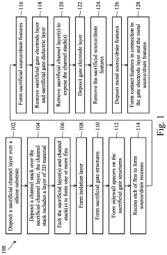
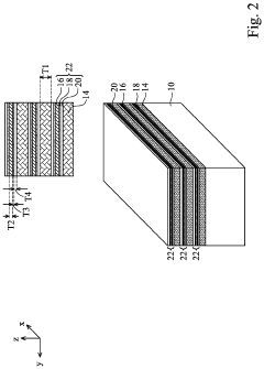
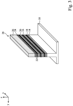
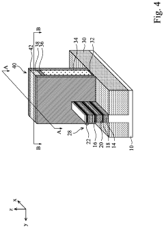
- The use of two-dimensional (2D) material nanosheets as channels in transistors, formed by alternately depositing sacrificial layers and channel stacks, which include a 2D material layer sandwiched between interfacial and high-k dielectric layers, enables higher mobility and reduced dimensions, allowing for increased drive current and integration density.
IP Strategy and Patent Landscape for 2D Semiconductors
The patent landscape for 2D semiconductors reveals a rapidly evolving intellectual property environment that demands strategic attention from industry players. Patent filings in this domain have experienced exponential growth since 2010, with a notable acceleration after 2015 when practical applications of 2D materials began demonstrating commercial potential. This growth trajectory indicates the technology's transition from purely academic research to industrial development.
Key patent holders currently include major technology corporations such as Samsung, IBM, and Intel, which collectively control approximately 35% of the global patent portfolio. However, academic institutions like MIT, Stanford University, and the Chinese Academy of Sciences have established significant IP positions, particularly in fundamental material properties and synthesis methods. This creates a complex licensing landscape that companies must navigate carefully.
Geographic distribution of patents shows interesting patterns, with the United States leading in application-specific patents while East Asian countries, particularly South Korea and China, dominate in manufacturing process innovations. European entities hold fewer patents but often focus on highly specialized applications with significant commercial potential.
Patent analysis reveals several strategic clusters forming around critical technology areas. These include synthesis and manufacturing methods (28% of patents), device architecture (23%), integration with conventional silicon technology (19%), and application-specific implementations (30%). The concentration of recent filings suggests that control over manufacturing scalability and integration techniques may become the determining factor for market leadership.
Freedom-to-operate challenges are emerging as the patent landscape becomes increasingly dense. Cross-licensing agreements between major players have begun to appear, indicating recognition of the need for collaborative approaches to commercialization. For new entrants, strategic patent acquisition or partnership with established patent holders may be necessary to avoid infringement risks.
Defensive patenting strategies are also evident, with companies securing broad claims around potential applications even before demonstrating technical feasibility. This approach aims to establish early barriers to competition in anticipation of future market development. Companies without robust patent portfolios may find themselves at a significant disadvantage as the technology matures toward mass-market applications.
Material Science Advancements Enabling 2D Semiconductor Development
The evolution of 2D semiconductors has been significantly propelled by breakthroughs in materials science. These advancements have transformed theoretical concepts into practical applications, enabling the development of ultra-thin semiconductor devices with exceptional properties. The foundation of this progress lies in novel synthesis methods that have overcome previous limitations in creating high-quality, large-area 2D semiconductor materials.
Chemical vapor deposition (CVD) techniques have undergone substantial refinement, as evidenced by patents focusing on controlled growth environments and precursor delivery systems. These innovations have addressed critical challenges in maintaining crystalline uniformity across larger substrates, essential for commercial viability. Molecular beam epitaxy (MBE) approaches have similarly advanced, with patented technologies enabling atomic-level precision in layering different 2D materials.
Defect engineering has emerged as another crucial area of materials science advancement. Patents reveal sophisticated methods for managing atomic vacancies, substitutions, and edge states that significantly influence carrier mobility and optical properties. These controlled defects can be strategically introduced to enhance specific performance characteristics rather than merely being minimized.
Substrate engineering represents a third pillar of materials science progress. Patent literature demonstrates innovative approaches to substrate preparation, including novel transfer techniques that preserve the integrity of 2D materials during device fabrication. The development of specialized substrates with tailored surface properties has enabled better lattice matching and reduced interfacial contamination.
Doping methodologies have also evolved substantially, with patents describing precise techniques for introducing carrier concentrations without disrupting the delicate 2D structure. These methods include plasma-assisted processes, intercalation approaches, and molecular adsorption techniques that offer unprecedented control over electrical properties.
Encapsulation and passivation technologies represent another critical advancement area, with patented solutions addressing the environmental sensitivity of many 2D materials. These protective strategies have extended device lifetimes while preserving the unique properties that make 2D semiconductors attractive for next-generation electronics.
The convergence of these materials science advancements has created a robust foundation for 2D semiconductor commercialization. Patent activity in this domain continues to accelerate, with increasing focus on scalable production methods and integration techniques compatible with existing semiconductor manufacturing infrastructure.
Unlock deeper insights with Patsnap Eureka Quick Research — get a full tech report to explore trends and direct your research. Try now!
Generate Your Research Report Instantly with AI Agent
Supercharge your innovation with Patsnap Eureka AI Agent Platform!