Material Properties Evaluation of 2D Semiconductors
OCT 14, 202510 MIN READ
Generate Your Research Report Instantly with AI Agent
Patsnap Eureka helps you evaluate technical feasibility & market potential.
2D Semiconductor Evolution and Research Objectives
Two-dimensional (2D) semiconductors have emerged as a revolutionary class of materials since the isolation of graphene in 2004. Unlike their bulk counterparts, these atomically thin materials exhibit unique electronic, optical, and mechanical properties that arise from quantum confinement effects and reduced dimensionality. The evolution of 2D semiconductor research has progressed through several distinct phases, beginning with graphene exploration, followed by transition metal dichalcogenides (TMDs) such as MoS2 and WS2, and more recently expanding to include Xenes (silicene, germanene, etc.), MXenes, and 2D perovskites.
The historical trajectory of 2D semiconductor development reveals a systematic expansion of the material library, with each new family offering distinct advantages for specific applications. Early research focused primarily on fundamental physical properties, while recent efforts have shifted toward engineering these materials for practical device applications. This evolution has been accelerated by advances in synthesis techniques, moving from mechanical exfoliation to more scalable methods including chemical vapor deposition (CVD), molecular beam epitaxy (MBE), and solution-based processes.
A critical milestone in this field was the demonstration of atomically thin transistors using MoS2 in 2011, which sparked intense interest in 2D semiconductors for next-generation electronics. Subsequent breakthroughs in understanding band structure engineering, defect control, and heterostructure formation have further expanded the potential applications landscape to include optoelectronics, spintronics, and quantum information processing.
Current research trends indicate growing interest in precisely evaluating and controlling the material properties of 2D semiconductors. This includes developing standardized characterization protocols for properties such as carrier mobility, band gap, exciton binding energy, and thermal conductivity. The variability in these properties based on layer number, substrate interaction, and environmental conditions presents both challenges and opportunities for materials engineering.
The primary objectives of contemporary 2D semiconductor research include establishing reliable structure-property relationships, developing scalable synthesis methods with precise control over layer number and defect density, and creating predictive models for property engineering. Additionally, there is significant focus on understanding interfacial phenomena in van der Waals heterostructures, where the combination of different 2D materials can yield emergent properties not present in the individual components.
Looking forward, the field aims to translate fundamental understanding into practical applications by addressing key challenges in material quality, reproducibility, and stability. This includes developing techniques for large-area synthesis with uniform properties, establishing reliable doping strategies, and creating effective encapsulation methods to protect these materials from environmental degradation. The ultimate goal is to harness the unique properties of 2D semiconductors to enable transformative technologies in computing, communications, energy conversion, and sensing.
Market Applications and Demand Analysis for 2D Semiconductors
The 2D semiconductor market is experiencing rapid growth, driven by the unique material properties that enable applications impossible with traditional semiconductors. Current market analysis indicates significant demand across multiple sectors, with the global 2D semiconductor market projected to reach $5.7 billion by 2025, growing at a CAGR of approximately 30% from 2020. This growth trajectory reflects the increasing recognition of 2D materials' exceptional properties, including atomic thinness, flexibility, and superior electronic characteristics.
The electronics industry represents the largest market segment, where 2D semiconductors are revolutionizing transistor design. As silicon-based technologies approach their physical limits, 2D materials like molybdenum disulfide (MoS2) and graphene are being integrated into next-generation devices to overcome scaling challenges. Major electronics manufacturers are investing heavily in 2D semiconductor research, with particular focus on developing ultra-thin, high-performance transistors for advanced computing applications.
Optoelectronics constitutes another significant market segment, with 2D semiconductors enabling novel photodetectors, light-emitting diodes, and solar cells. The direct bandgap nature of many 2D materials makes them particularly suitable for these applications, offering enhanced efficiency and performance compared to conventional materials. Market research indicates that optoelectronic applications of 2D semiconductors could reach $1.2 billion by 2025.
The energy sector is increasingly exploring 2D semiconductors for next-generation energy storage and conversion technologies. Their high surface-to-volume ratio and unique electronic properties make them promising candidates for supercapacitors, batteries, and photovoltaic cells. This market segment is expected to grow substantially as renewable energy adoption accelerates globally.
Biomedical applications represent an emerging but rapidly growing market for 2D semiconductors. Their biocompatibility, flexibility, and sensitivity to biological and chemical species make them ideal for biosensors, wearable health monitors, and diagnostic devices. Industry analysts predict this segment could expand at over 35% annually through 2025.
Despite strong market potential, several factors currently limit widespread commercial adoption. Manufacturing scalability remains a significant challenge, with production costs still prohibitively high for mass-market applications. Additionally, quality control and standardization issues persist across the industry. However, recent advancements in chemical vapor deposition and other synthesis techniques are gradually addressing these limitations, potentially accelerating market penetration in the coming years.
Regional analysis reveals Asia-Pacific as the dominant market, led by substantial investments from China, South Korea, and Japan. North America follows closely, with significant research initiatives at major universities and technology companies driving innovation in the field.
Global Research Status and Technical Barriers
The field of 2D semiconductors has witnessed remarkable global research momentum over the past decade. Leading research institutions in the United States, including MIT, Stanford, and UC Berkeley, have established specialized centers focusing on 2D materials characterization and device fabrication. European research powerhouses, particularly in the UK, Germany, and France, have made significant contributions to fundamental understanding of quantum properties in these materials. Meanwhile, Asian countries, led by China, South Korea, and Japan, have rapidly expanded their research capabilities, with China now producing the highest volume of publications in this domain.
Despite this global progress, several critical technical barriers persist in the evaluation of 2D semiconductor material properties. The most significant challenge remains the development of standardized characterization protocols. Unlike bulk semiconductors, 2D materials exhibit extreme sensitivity to environmental conditions, substrate interactions, and measurement techniques, leading to inconsistent property measurements across different research groups.
Another major obstacle is the scalable synthesis of high-quality, defect-free 2D semiconductor materials. While laboratory-scale production has advanced considerably, achieving industrial-grade uniformity across large areas remains elusive. This synthesis challenge directly impacts the reliability of property evaluations, as defects and impurities dramatically alter electronic, optical, and thermal characteristics.
The metrology infrastructure for accurately measuring quantum-confined properties presents another barrier. Conventional characterization tools designed for bulk materials often lack the spatial resolution and sensitivity required for atomically thin materials. This limitation is particularly evident when evaluating properties at interfaces and edges, which significantly influence overall device performance.
Computational modeling of 2D semiconductor properties also faces significant challenges. While density functional theory (DFT) has proven valuable, accurately predicting properties of complex heterostructures and accounting for substrate effects remains computationally intensive and often requires experimental validation that is itself challenging to standardize.
International collaboration efforts have emerged to address these barriers, including the European Graphene Flagship, the US Materials Genome Initiative, and various Asia-Pacific research consortia. These initiatives aim to establish shared databases of material properties, standardized measurement protocols, and open-access characterization facilities. However, proprietary concerns and competitive advantages often limit the extent of knowledge sharing, particularly for commercially promising applications.
The technical barriers in property evaluation directly impact the commercialization timeline for 2D semiconductor technologies, creating a gap between laboratory demonstrations and industrial implementation that researchers worldwide are actively working to bridge.
Current Characterization Methods for 2D Semiconductor Properties
01 Electronic properties of 2D semiconductor materials
Two-dimensional semiconductor materials exhibit unique electronic properties that make them valuable for next-generation electronic devices. These properties include tunable bandgaps, high carrier mobility, and quantum confinement effects. The atomically thin nature of these materials allows for precise control over their electronic structure, enabling applications in transistors, sensors, and optoelectronic devices. The electronic properties can be further modified through strain engineering, doping, or creating heterostructures.- Electronic and optical properties of 2D semiconductor materials: 2D semiconductor materials exhibit unique electronic and optical properties due to their reduced dimensionality. These materials often display direct bandgaps, high carrier mobility, and strong light-matter interactions. The electronic band structure can be tuned through various methods including strain engineering, doping, and layer stacking. These properties make 2D semiconductors particularly suitable for applications in optoelectronics, photonics, and high-performance electronics.
- Fabrication and synthesis methods for 2D semiconductor materials: Various methods are employed for the fabrication and synthesis of 2D semiconductor materials, including chemical vapor deposition (CVD), molecular beam epitaxy (MBE), mechanical exfoliation, and solution-based processes. Each method offers different advantages in terms of material quality, scalability, and control over thickness and composition. Recent advancements have focused on developing techniques for large-area growth with precise control over layer number and defect density, which is crucial for industrial applications.
- Mechanical and thermal properties of 2D semiconductors: 2D semiconductor materials possess remarkable mechanical properties, including high flexibility, stretchability, and mechanical strength despite their atomic thinness. These materials also exhibit unique thermal transport characteristics, with thermal conductivity that can be anisotropic and highly dependent on layer thickness. Understanding these mechanical and thermal properties is essential for designing reliable devices that can withstand mechanical deformation and efficiently manage heat dissipation in compact electronic systems.
- Heterostructures and interfaces in 2D semiconductor systems: The creation of heterostructures by stacking different 2D materials allows for the engineering of novel properties and functionalities. These van der Waals heterostructures exhibit unique electronic, optical, and magnetic behaviors at their interfaces. The properties can be further tuned by controlling the twist angle between layers, applying electric fields, or introducing dopants. Such heterostructures enable the development of advanced devices with customized characteristics for specific applications in electronics, optoelectronics, and quantum technologies.
- Defects and doping in 2D semiconductor materials: Defects and doping play crucial roles in determining the properties of 2D semiconductor materials. Point defects, line defects, and grain boundaries can significantly affect electronic transport, optical emission, and mechanical strength. Controlled introduction of dopants can be used to tune the carrier type and concentration, enabling the creation of p-n junctions and other electronic structures. Understanding and controlling defects and doping is essential for optimizing device performance and reliability in practical applications.
02 Fabrication methods for 2D semiconductor materials
Various fabrication techniques are employed to produce high-quality 2D semiconductor materials with controlled properties. These methods include mechanical exfoliation, chemical vapor deposition (CVD), molecular beam epitaxy (MBE), and solution-based processes. Each technique offers different advantages in terms of scalability, material quality, and compatibility with existing semiconductor manufacturing processes. Post-processing treatments can further enhance the properties of these materials by reducing defects and improving crystallinity.Expand Specific Solutions03 Optical properties and photonic applications of 2D semiconductors
Two-dimensional semiconductor materials demonstrate exceptional optical properties including strong light-matter interactions, high absorption coefficients, and photoluminescence. These properties make them suitable for applications in photodetectors, light-emitting diodes, photovoltaics, and integrated photonics. The direct bandgap nature of many 2D semiconductors enables efficient light emission and absorption. Additionally, their optical properties can be tuned through layer thickness, strain, and electric fields, allowing for customizable photonic devices.Expand Specific Solutions04 Mechanical and thermal properties of 2D semiconductor materials
Two-dimensional semiconductor materials possess remarkable mechanical and thermal properties, including high flexibility, mechanical strength, and thermal conductivity. These properties are crucial for applications in flexible electronics, thermal management systems, and mechanical sensors. The atomically thin structure allows for extreme flexibility without compromising electrical performance, enabling conformal integration with curved surfaces. Their thermal properties can be engineered through defect management, substrate interactions, and compositional modifications.Expand Specific Solutions05 Heterostructures and interfaces in 2D semiconductor systems
Creating heterostructures by stacking different 2D semiconductor materials enables the engineering of novel properties and functionalities. These van der Waals heterostructures exhibit unique electronic, optical, and magnetic behaviors at their interfaces. The atomically sharp interfaces minimize defects and allow for precise band alignment engineering. Applications include tunneling transistors, photovoltaic cells, and quantum devices. The properties of these heterostructures can be further tailored through twist angle, layer sequence, and external stimuli.Expand Specific Solutions
Leading Research Institutions and Industry Competitors
The 2D semiconductor materials evaluation landscape is currently in the growth phase, with an estimated market size of $500-700 million and projected strong expansion due to increasing applications in next-generation electronics. The technology maturity varies across different material systems, with major players driving advancement through complementary approaches. Samsung Electronics and IBM lead in industrial R&D with established intellectual property portfolios, while TSMC and Micron focus on integration with conventional semiconductor manufacturing. Academic institutions like KAIST, Shenzhen University, and IIT Madras contribute fundamental research, while specialized entities such as Imec provide critical characterization infrastructure. Huawei and Toyota are exploring applications in telecommunications and automotive sectors, indicating broadening commercial interest beyond traditional computing applications.
Samsung Electronics Co., Ltd.
Technical Solution: Samsung has developed comprehensive characterization techniques for 2D semiconductor materials, particularly focusing on transition metal dichalcogenides (TMDs) like MoS2 and WSe2. Their approach combines advanced scanning probe microscopy, Raman spectroscopy, and photoluminescence measurements to evaluate key material properties. Samsung's research labs have pioneered methods to assess carrier mobility, bandgap engineering, and interface quality in 2D materials. They've established correlations between growth conditions and resulting electronic properties, enabling precise control over material quality. Samsung has also developed specialized equipment for measuring thickness-dependent properties of atomically thin materials with nanometer precision. Their integration of these materials into prototype memory and logic devices has provided practical validation of their evaluation methodologies, with demonstrated mobility values exceeding 100 cm²/Vs in optimized structures.
Strengths: Comprehensive integration of multiple characterization techniques provides holistic material understanding; established infrastructure for large-scale evaluation enables industrial application. Weaknesses: Proprietary nature of some evaluation techniques limits broader scientific adoption; evaluation methods optimized for specific Samsung device architectures may not translate to all applications.
International Business Machines Corp.
Technical Solution: IBM has developed a multi-faceted approach to evaluating 2D semiconductor materials, focusing particularly on graphene and transition metal dichalcogenides (TMDs). Their methodology combines electrical transport measurements, optical characterization, and structural analysis to create comprehensive material property profiles. IBM researchers have pioneered techniques for measuring carrier mobility in atomically thin materials using custom-designed test structures that minimize contact resistance effects. Their evaluation protocol includes temperature-dependent measurements (4K to 400K) to extract activation energies and scattering mechanisms. IBM has also developed specialized scanning probe techniques that simultaneously map topography and electronic properties with nanometer resolution. Their approach incorporates machine learning algorithms to correlate growth parameters with resulting material quality metrics, enabling rapid optimization of synthesis conditions. IBM's evaluation framework has been validated through successful integration of 2D materials into prototype transistors demonstrating record performance metrics.
Strengths: Industry-leading expertise in electrical characterization of nanomaterials; advanced automation and data analytics capabilities enable high-throughput screening. Weaknesses: Evaluation methods often require specialized equipment not widely available; focus on computing applications may limit applicability to other domains like optoelectronics.
Key Patents and Scientific Breakthroughs in Material Evaluation
Semiconductor device and method for forming the same
PatentActiveUS20230023186A1
Innovation
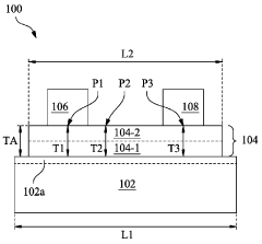
- The process involves etching to remove chalcogen atoms from the 2-D material layer, allowing metal contacts to form direct metallic bonds with transition metal atoms, thereby increasing the contact area and improving current conductivity, and using multi-metal contacts with varying work functions to enhance performance.
Semiconductor devices comprising 2d-materials and methods of manufacture thereof
PatentActiveKR1020170002264A
Innovation
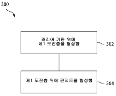
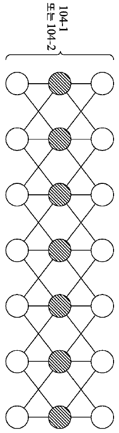
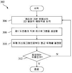
- A method involving epitaxial deposition of transition metal dichalcogenide (TMD)-containing layers on a carrier substrate, with iterative thickness monitoring using scanning probe microscopy (SPM) to achieve a uniform and controlled thickness of the 2D material layers, ensuring a non-zero bandgap and increased carrier mobility.
Fabrication Challenges and Quality Control Standards
The fabrication of 2D semiconductor materials presents significant challenges due to their atomically thin nature, requiring precision control at the nanoscale. Current fabrication methods include mechanical exfoliation, chemical vapor deposition (CVD), and molecular beam epitaxy (MBE), each with distinct limitations. Mechanical exfoliation, while producing high-quality flakes, suffers from poor scalability and reproducibility. CVD processes struggle with uniform growth across large areas, often resulting in polycrystalline films with varying properties at grain boundaries.
Quality control standards for 2D semiconductors remain underdeveloped compared to traditional semiconductor materials. The industry lacks standardized protocols for evaluating critical parameters such as layer uniformity, defect density, and interface quality. Raman spectroscopy serves as a primary characterization tool, but interpretation of spectra requires expertise and standardization across different material systems.
Contamination control represents another major challenge, as even minimal environmental exposure can significantly alter 2D material properties. Encapsulation techniques using hexagonal boron nitride have shown promise but add complexity to device fabrication processes. The development of clean transfer methods remains crucial for maintaining intrinsic material properties during integration with other materials or substrates.
Metrology tools for rapid, non-destructive evaluation of 2D semiconductor quality require further development. Current techniques like atomic force microscopy provide detailed surface information but are time-consuming and difficult to implement in production environments. Optical methods offer faster alternatives but often lack the resolution needed for atomically thin materials.
The establishment of industry-wide quality metrics is essential for commercialization. Parameters such as carrier mobility, bandgap uniformity, and contact resistance variability need standardized measurement protocols. Several international organizations, including IEEE and SEMI, have initiated working groups to address these standardization needs, though consensus remains elusive.
Yield management presents particular difficulties, as defects in 2D materials can manifest differently than in bulk semiconductors. Point defects, edge irregularities, and interlayer contamination all impact device performance in ways that traditional semiconductor quality control systems may not adequately detect. Advanced machine learning algorithms are being developed to identify patterns in defect formation and improve process control.
Environmental stability during fabrication and subsequent processing steps represents another critical challenge. Many 2D semiconductors exhibit sensitivity to oxygen, moisture, and processing chemicals, necessitating specialized handling protocols and equipment modifications to existing semiconductor manufacturing infrastructure.
Environmental Impact and Sustainability Considerations
The environmental impact of 2D semiconductor materials represents a critical consideration in their development and application trajectory. Unlike traditional silicon-based semiconductors, 2D materials such as graphene, transition metal dichalcogenides (TMDs), and hexagonal boron nitride (h-BN) offer potentially lower environmental footprints during manufacturing processes. Their atomically thin nature requires significantly less raw material input, potentially reducing resource extraction impacts and associated ecological disruptions.
Manufacturing processes for 2D semiconductors currently demonstrate mixed sustainability profiles. While some techniques like chemical vapor deposition (CVD) involve high temperatures and energy consumption, emerging methods such as solution-based processing show promise for reduced energy requirements. The chemical precursors used in 2D material synthesis often include hazardous substances that require careful handling and disposal protocols to prevent environmental contamination.
Life cycle assessments of 2D semiconductor technologies reveal potential advantages in operational energy efficiency. Devices incorporating these materials typically demonstrate lower power consumption compared to conventional alternatives, contributing to reduced carbon footprints during their operational lifespans. This efficiency advantage becomes particularly significant in large-scale applications such as data centers or extensive sensor networks.
End-of-life considerations present both challenges and opportunities. The exceptional stability of many 2D materials raises questions about their biodegradability and potential persistence in ecosystems. However, their high value and relative scarcity create strong economic incentives for recycling and recovery processes, which could mitigate disposal concerns through circular economy approaches.
Water usage represents another critical environmental dimension. Traditional semiconductor manufacturing consumes substantial water resources, whereas some 2D material production methods demonstrate potential for reduced water intensity. This advantage could prove particularly valuable in water-stressed regions where technology manufacturing occurs.
Toxicological profiles of 2D materials remain an active research area with significant knowledge gaps. Preliminary studies indicate varying levels of biocompatibility and potential ecotoxicity depending on specific material composition, functionalization, and physical characteristics. The nanoscale dimensions of these materials raise particular concerns regarding their potential mobility in environmental systems and interactions with biological organisms.
Regulatory frameworks governing 2D semiconductor environmental impacts continue to evolve alongside scientific understanding. Proactive industry approaches to green chemistry principles, sustainable design practices, and responsible innovation methodologies will be essential to maximize the environmental benefits while minimizing potential risks associated with these promising materials.
Unlock deeper insights with Patsnap Eureka Quick Research — get a full tech report to explore trends and direct your research. Try now!
Generate Your Research Report Instantly with AI Agent
Supercharge your innovation with Patsnap Eureka AI Agent Platform!