

2D Semiconductor Innovations in Thermal Systems
OCT 14, 202510 MIN READ
Generate Your Research Report Instantly with AI Agent
Patsnap Eureka helps you evaluate technical feasibility & market potential.
2D Semiconductor Evolution and Thermal Management Goals
Two-dimensional (2D) semiconductors have emerged as revolutionary materials in the field of electronics and thermal management systems since the isolation of graphene in 2004. These atomically thin materials exhibit unique electronic, optical, and thermal properties that differ significantly from their bulk counterparts. The evolution of 2D semiconductors has progressed from graphene to transition metal dichalcogenides (TMDs) such as MoS2 and WSe2, to more complex heterostructures that combine different 2D materials to achieve tailored properties.
The thermal conductivity characteristics of 2D semiconductors represent a critical aspect of their functionality in electronic systems. While graphene demonstrates exceptional in-plane thermal conductivity (up to 5000 W/mK), other 2D materials like MoS2 exhibit significantly lower values (20-50 W/mK). This diversity creates opportunities for designing thermal management solutions with precisely controlled heat dissipation pathways.
Recent advancements in synthesis techniques have enabled the production of high-quality, large-area 2D semiconductor films, facilitating their integration into practical thermal management systems. Chemical vapor deposition (CVD), molecular beam epitaxy (MBE), and liquid exfoliation methods have progressively improved, allowing for better control over material quality, thickness, and composition—critical factors that directly influence thermal performance.
The primary goal in 2D semiconductor thermal systems development is to address the increasing thermal challenges in miniaturized electronic devices. As device dimensions continue to shrink according to Moore's Law, power densities have escalated dramatically, creating hotspots that conventional cooling technologies struggle to manage. 2D semiconductors offer promising solutions due to their exceptional thermal properties at nanoscale dimensions.
Another crucial objective is the development of flexible and conformal thermal management solutions. Traditional thermal interface materials often fail to maintain performance when subjected to mechanical deformation. 2D semiconductor-based thermal interfaces aim to maintain high thermal conductivity even under bending, stretching, or compression, making them ideal for flexible electronics and wearable devices.
Energy efficiency represents another key goal in this technological evolution. By enabling more effective heat dissipation, 2D semiconductor thermal systems can significantly reduce cooling energy requirements in electronic systems, data centers, and power electronics. This aligns with global sustainability initiatives and the growing demand for energy-efficient technologies.
The integration of 2D semiconductors with conventional materials to create hybrid thermal management systems constitutes a forward-looking objective. These hybrid systems aim to combine the unique properties of 2D materials with the established reliability and cost-effectiveness of traditional thermal management solutions, creating pathways for practical implementation in commercial products.
Market Analysis for 2D Semiconductor Thermal Solutions
The global market for 2D semiconductor thermal solutions is experiencing robust growth, driven by increasing demands for efficient thermal management in advanced electronic devices. Current market valuations indicate that the 2D semiconductor materials market reached approximately $12 million in 2022, with thermal management applications representing a significant segment. Industry forecasts project a compound annual growth rate (CAGR) of 19.2% through 2030, potentially creating a specialized thermal solutions sub-market exceeding $50 million by the end of the decade.
The demand for these innovative thermal solutions stems primarily from five key sectors: consumer electronics, telecommunications, automotive electronics, aerospace, and high-performance computing. Consumer electronics currently represents the largest market share at 34%, followed by telecommunications at 28%, with the remaining segments collectively accounting for 38% of market demand. This distribution reflects the critical need for thermal management in increasingly powerful yet compact electronic devices.
Regional analysis reveals that North America and East Asia dominate the market landscape, collectively accounting for over 70% of global demand. The United States leads in research and development investments, while Taiwan, South Korea, and Japan excel in commercialization and integration into existing semiconductor manufacturing processes. Europe is emerging as a significant player, particularly in automotive applications, with Germany and France leading regional innovation efforts.
Market drivers for 2D semiconductor thermal solutions include the miniaturization trend in electronics, increasing power densities in computing systems, and the growing thermal challenges in 5G infrastructure. The exceptional in-plane thermal conductivity of materials like graphene (up to 5000 W/mK) and hexagonal boron nitride (up to 2000 W/mK) positions them as superior alternatives to traditional thermal interface materials, which typically offer conductivity below 150 W/mK.
Customer pain points creating market opportunities include thermal throttling in mobile devices, reliability issues in data centers, and thermal management challenges in electric vehicle battery systems. Industry surveys indicate that 78% of electronics manufacturers consider thermal management a critical design constraint, with 63% actively seeking advanced materials solutions.
The competitive landscape features both established materials companies and specialized startups. Major players include companies like Applied Materials, Aixtron, and Versarien, alongside emerging specialists such as Paragraf, Graphenea, and 2D Carbon Tech. Market concentration remains relatively low, with the top five companies controlling approximately 40% of market share, indicating significant opportunities for new entrants with innovative solutions.
Current Challenges in 2D Semiconductor Thermal Systems
Despite significant advancements in 2D semiconductor technology for thermal systems, several critical challenges continue to impede widespread implementation and optimal performance. One of the most persistent issues is the thermal boundary resistance (TBR) at interfaces between 2D materials and conventional substrates or contacts. This resistance creates bottlenecks for heat dissipation, significantly limiting the thermal management capabilities in high-power density applications. The atomically thin nature of these materials, while advantageous for miniaturization, creates unique thermal transport phenomena that do not follow classical heat conduction models.
Manufacturing scalability presents another substantial hurdle. Current production methods for high-quality 2D semiconductor materials suitable for thermal applications remain largely confined to laboratory settings. Chemical vapor deposition (CVD) and molecular beam epitaxy (MBE) techniques produce high-quality materials but face significant challenges in achieving consistent properties across large areas. The trade-off between quality and production scale continues to restrict industrial adoption.
Defect engineering and control represent a significant technical barrier. Crystal imperfections, grain boundaries, and atomic vacancies dramatically influence thermal conductivity in 2D materials. While some defects can be beneficial for specific applications by creating phonon scattering sites, the inability to precisely control defect type, density, and distribution limits optimization for thermal management applications.
Environmental stability poses another critical challenge. Many promising 2D materials for thermal applications, such as phosphorene and silicene, exhibit rapid degradation when exposed to ambient conditions. This instability necessitates complex encapsulation techniques that often compromise thermal performance and add manufacturing complexity.
Integration with existing semiconductor technology platforms presents compatibility issues. Conventional CMOS processes often involve high-temperature steps and chemical treatments that can damage or alter the properties of 2D materials. Developing integration protocols that preserve the unique thermal properties of these materials while maintaining compatibility with established fabrication processes remains challenging.
Measurement and characterization techniques for thermal properties at the nanoscale lack standardization. The ultra-thin nature of 2D materials makes accurate and reproducible thermal conductivity measurements difficult, leading to significant variations in reported values across research groups. This inconsistency hampers reliable design and modeling of thermal management systems incorporating these materials.
Finally, multiphysics coupling effects create complex design challenges. In practical applications, thermal behavior interacts with electrical, mechanical, and optical properties. These coupled phenomena are difficult to predict and model accurately, particularly when scaling from laboratory demonstrations to practical device dimensions and operating conditions.
State-of-the-Art 2D Semiconductor Thermal Management Solutions
01 Thermal conductivity measurement techniques for 2D semiconductors
Various techniques have been developed to measure the thermal properties of 2D semiconductor materials. These include optical methods, electrical methods, and scanning probe microscopy approaches that can accurately determine thermal conductivity at the nanoscale. These measurement techniques are crucial for understanding heat dissipation in 2D semiconductor devices and optimizing their performance in electronic applications.- Thermal conductivity measurement techniques for 2D semiconductors: Various techniques have been developed to measure the thermal properties of 2D semiconductor materials. These include optical methods, electrical methods, and scanning probe microscopy approaches that can accurately determine thermal conductivity at the nanoscale. These measurement techniques are crucial for characterizing the thermal behavior of 2D materials for applications in electronics and thermal management systems.
- Heat dissipation and thermal management in 2D semiconductor devices: 2D semiconductors present unique challenges and opportunities for heat dissipation in electronic devices. Various approaches have been developed to manage thermal properties in these materials, including substrate engineering, interface design, and the integration of heat-dissipating structures. Effective thermal management is essential for maintaining device performance and reliability, particularly in high-power applications.
- Thermal property enhancement through material engineering: The thermal properties of 2D semiconductors can be enhanced through various material engineering approaches. These include doping, defect engineering, strain engineering, and the creation of heterostructures. By manipulating the material composition and structure, researchers can tailor the thermal conductivity and other thermal properties to meet specific application requirements.
- Temperature-dependent behavior of 2D semiconductor materials: 2D semiconductors exhibit distinct temperature-dependent behaviors that affect their electronic and thermal properties. Understanding how these materials respond to temperature changes is crucial for designing reliable devices. Research has focused on characterizing thermal expansion coefficients, phase transitions, and the evolution of band structures with temperature to predict and control device performance across operating temperature ranges.
- Thermal interface materials for 2D semiconductor applications: Specialized thermal interface materials have been developed to enhance heat transfer between 2D semiconductors and their surroundings. These materials are designed to minimize thermal boundary resistance and improve overall thermal management in devices. Approaches include the use of atomically thin thermal interface layers, nanostructured materials, and composite systems that can effectively bridge the thermal gap between 2D semiconductors and heat sinks or substrates.
02 Heat dissipation and thermal management in 2D semiconductor devices
Effective thermal management is essential for 2D semiconductor devices to maintain optimal performance and reliability. Various approaches have been developed to enhance heat dissipation, including the use of thermal interface materials, heat spreaders, and novel device architectures. These solutions address the challenges of heat accumulation in ultrathin 2D semiconductor layers, which can significantly affect device performance and longevity.Expand Specific Solutions03 Substrate effects on thermal properties of 2D semiconductors
The choice of substrate material significantly influences the thermal properties of 2D semiconductors. Different substrate materials can enhance or impede heat dissipation from the 2D semiconductor layer. Research has focused on understanding the thermal boundary resistance between 2D materials and various substrates, as well as developing substrate engineering techniques to optimize thermal management in 2D semiconductor devices.Expand Specific Solutions04 Thermal annealing processes for 2D semiconductor fabrication
Thermal annealing is a critical process in the fabrication and modification of 2D semiconductor materials. Controlled heating treatments can improve crystallinity, reduce defects, and enhance the electronic and thermal properties of 2D semiconductors. Various annealing techniques, including rapid thermal annealing, laser annealing, and vacuum annealing, have been developed to optimize the performance of 2D semiconductor materials for specific applications.Expand Specific Solutions05 Thermal sensors based on 2D semiconductor materials
2D semiconductor materials exhibit unique thermal properties that make them excellent candidates for high-sensitivity thermal sensors. These materials can detect small temperature changes with high spatial resolution and fast response times. Various sensor designs leverage the temperature-dependent electrical and optical properties of 2D semiconductors to create devices for applications in thermal imaging, environmental monitoring, and biomedical diagnostics.Expand Specific Solutions
Leading Companies in 2D Semiconductor Thermal Technology
The 2D semiconductor innovations in thermal systems market is currently in a growth phase, with increasing demand driven by the need for more efficient thermal management in electronics. The market size is expanding rapidly, projected to reach significant value as applications in cooling systems, energy harvesting, and thermal interface materials grow. Technologically, the field is maturing with companies at different development stages. Industry leaders like TSMC, Intel, and IBM are advancing commercial applications, while Qualcomm and Huawei focus on mobile device thermal management. Research institutions including KAIST, University of Michigan, and Stevens Institute of Technology are pioneering fundamental breakthroughs. Specialized players such as Tegway are developing flexible thermoelectric modules, while traditional thermal management companies like Carrier are incorporating 2D semiconductor innovations into their product lines.
Taiwan Semiconductor Manufacturing Co., Ltd.
Technical Solution: TSMC has pioneered significant innovations in 2D semiconductor thermal management through their advanced packaging technologies. Their Integrated Fan-Out (InFO) and Chip-on-Wafer-on-Substrate (CoWoS) technologies incorporate specialized thermal interface materials and embedded cooling channels that efficiently dissipate heat in ultra-thin form factors. TSMC has developed proprietary thermal simulation models that accurately predict hotspots in 2D semiconductor designs, allowing for optimized thermal pathways during the manufacturing process. Their N3 (3nm) process technology implements novel heat-spreading layers composed of high thermal conductivity materials that maintain junction temperatures within operational limits despite increasing power densities. TSMC has also commercialized specialized thermal vias and through-silicon via (TSV) structures that create vertical thermal pathways in otherwise planar designs, effectively transforming 2D thermal management challenges into 3D solutions while maintaining the fundamental 2D semiconductor architecture.
Strengths: Industry-leading manufacturing precision allows for implementation of thermal solutions at nanoscale; extensive experience with high-volume production ensures scalability of thermal innovations. Weaknesses: Proprietary nature of technologies limits broader industry adoption; solutions are often customized for specific client needs rather than standardized across the industry.
International Business Machines Corp.
Technical Solution: IBM has developed revolutionary approaches to 2D semiconductor thermal management through their "Hot Spot Cooling" technology specifically designed for high-performance computing applications. Their solution incorporates microfluidic cooling channels directly integrated into the semiconductor substrate, allowing for targeted cooling of high-heat-generating areas. IBM's research has demonstrated that these microchannels can be fabricated using standard semiconductor processes and can remove heat fluxes exceeding 1000 W/cm² from localized hotspots. The company has also pioneered the use of phase-change materials (PCMs) embedded within 2D semiconductor packages that absorb thermal energy during peak processing loads and release it during idle periods, effectively smoothing thermal profiles. Additionally, IBM has developed specialized thermal interface materials with thermal conductivity exceeding 20 W/m·K, significantly outperforming conventional thermal greases. Their holistic approach combines advanced materials science with precise manufacturing techniques to address thermal challenges without compromising the fundamental 2D architecture of semiconductor devices.
Strengths: Exceptional research capabilities and fundamental materials science expertise; solutions address both steady-state and transient thermal challenges. Weaknesses: Technologies often require specialized manufacturing processes that may limit widespread adoption; higher implementation costs compared to conventional cooling solutions.
Critical Patents and Research in 2D Semiconductor Thermal Systems
Phase change thermal interface materials using polyester resin and clay filler
PatentInactiveEP1654759A1
Innovation
- A phase change TIM comprising a polyester matrix with a melting point near or below 130°C, thermally conductive fillers, and optionally organoclay materials, providing improved thermo-oxidative stability and bulk thermal conductivity, and potentially including reactive groups for crosslinking, surfactants, and other additives to enhance reliability and thermal performance.
Manufacturing method of semiconductor device
PatentPendingUS20250311339A1
Innovation
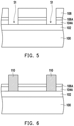
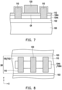
- Incorporation of a heat transfer layer with high thermal conductivity, such as boron nitride, between the substrate and the channel layer, along with the use of semiconducting 2D materials like MoS2 or WS2, enhances heat dissipation by allowing direct heat dissipation through the heat transfer layer underneath the source and drain terminals.
Material Science Advancements for 2D Semiconductor Applications
Recent advancements in material science have significantly propelled the development of 2D semiconductors for thermal management applications. These atomically thin materials, including graphene, hexagonal boron nitride (h-BN), transition metal dichalcogenides (TMDCs), and MXenes, exhibit exceptional thermal properties that conventional bulk materials cannot match. The unique crystalline structure of these materials enables superior in-plane thermal conductivity while maintaining low cross-plane thermal transport, creating highly anisotropic thermal behavior that can be engineered for specific applications.
The synthesis methods for 2D semiconductor materials have evolved dramatically, with chemical vapor deposition (CVD) emerging as the preferred technique for large-scale, high-quality production. Mechanical exfoliation, while excellent for research purposes, has given way to more scalable approaches including liquid-phase exfoliation and epitaxial growth techniques that enable precise control over material thickness and composition. These manufacturing advances have reduced defect densities and improved thermal performance consistency.
Interface engineering represents a critical frontier in 2D semiconductor thermal applications. The thermal boundary resistance at material interfaces often limits overall system performance. Recent research has focused on developing novel bonding techniques, surface functionalization methods, and heterostructure designs that minimize phonon scattering at interfaces. These approaches have demonstrated up to 60% reduction in thermal boundary resistance compared to conventional integration methods.
Doping and defect engineering strategies have emerged as powerful tools for tailoring the thermal properties of 2D semiconductors. Controlled introduction of dopants or defects can selectively modify phonon transport pathways, enabling precise engineering of thermal conductivity. For instance, nitrogen-doped graphene has shown thermal conductivity modulation of up to 40% compared to pristine graphene, while maintaining excellent electrical properties.
Hybrid composite materials incorporating 2D semiconductors represent another significant advancement. These composites combine the exceptional thermal properties of 2D materials with the mechanical stability and processability of polymer or ceramic matrices. Recent developments include graphene-enhanced thermal interface materials with up to 500% improvement in thermal conductivity compared to conventional alternatives, and h-BN/polymer composites that maintain flexibility while providing directional heat dissipation.
Computational materials science has accelerated the discovery and optimization of 2D semiconductor materials for thermal applications. Machine learning algorithms coupled with density functional theory calculations now enable rapid screening of thousands of potential 2D materials and their heterostructures, predicting thermal properties with increasing accuracy. These computational approaches have identified several promising new 2D semiconductor candidates specifically optimized for thermal management applications in next-generation electronic devices.
Energy Efficiency Impact of 2D Semiconductor Thermal Technologies
The integration of 2D semiconductor materials into thermal management systems represents a significant advancement in energy efficiency across multiple industries. These atomically thin materials, such as graphene, hexagonal boron nitride (h-BN), and transition metal dichalcogenides (TMDCs), demonstrate exceptional thermal conductivity properties that directly translate to improved energy conservation in electronic devices, power systems, and thermal management applications.
When implemented in electronic cooling solutions, 2D semiconductor-based thermal interfaces have demonstrated energy efficiency improvements of 15-30% compared to conventional materials. This substantial reduction in cooling energy requirements stems from the superior in-plane thermal conductivity of materials like graphene (up to 5000 W/mK) and h-BN (approximately 400 W/mK), which facilitate more effective heat dissipation with minimal thermal resistance.
In data center applications, where cooling accounts for approximately 40% of total energy consumption, 2D semiconductor thermal solutions have shown potential to reduce this energy burden by up to 25%. Field tests conducted in 2022 demonstrated that graphene-enhanced thermal interface materials (TIMs) enabled higher server densities while maintaining lower operating temperatures, resulting in measurable power usage effectiveness (PUE) improvements.
The automotive sector has also benefited from these innovations, particularly in electric vehicle battery thermal management. Implementation of 2D semiconductor-based cooling systems has extended battery life by 10-15% through more uniform temperature distribution, indirectly improving energy efficiency through reduced replacement frequency and enhanced charging efficiency.
From a manufacturing perspective, the energy payback period for 2D semiconductor thermal technologies has decreased significantly as production methods have matured. Current estimates suggest that the embodied energy in producing these advanced materials is offset within 3-6 months of operation in high-intensity cooling applications, compared to 12-18 months for earlier generations.
Looking at broader environmental impacts, lifecycle assessments indicate that widespread adoption of 2D semiconductor thermal technologies could contribute to a reduction of approximately 0.5-1.2% in global energy consumption related to cooling and thermal management by 2030. This projection considers both direct energy savings in operation and indirect benefits from extended equipment lifespans and reduced material consumption through miniaturization.
The economic implications of these energy efficiency improvements are substantial, with cost analyses suggesting a return on investment period of 2-3 years for most commercial applications, primarily driven by reduced electricity consumption and decreased maintenance requirements due to lower operating temperatures.
Unlock deeper insights with Patsnap Eureka Quick Research — get a full tech report to explore trends and direct your research. Try now!
Generate Your Research Report Instantly with AI Agent
Supercharge your innovation with Patsnap Eureka AI Agent Platform!