

Advanced Coating Techniques for 2D Semiconductor Applications
OCT 14, 20259 MIN READ
Generate Your Research Report Instantly with AI Agent
Patsnap Eureka helps you evaluate technical feasibility & market potential.
2D Semiconductor Coating Background and Objectives
Two-dimensional (2D) semiconductors have emerged as revolutionary materials in the field of electronics and optoelectronics since the isolation of graphene in 2004. These atomically thin materials, including transition metal dichalcogenides (TMDs) like MoS2, WS2, and WSe2, as well as black phosphorus and hexagonal boron nitride (h-BN), exhibit unique electronic, optical, and mechanical properties that differ significantly from their bulk counterparts. The ultrathin nature of these materials creates quantum confinement effects that result in direct bandgaps, enhanced carrier mobility, and exceptional flexibility, making them promising candidates for next-generation electronic devices.
The evolution of 2D semiconductor technology has progressed from initial fundamental research to potential commercial applications over the past decade. Early research focused primarily on graphene's extraordinary properties, but attention has since expanded to a broader family of 2D materials with diverse characteristics. This technological progression has been driven by advances in synthesis methods, characterization techniques, and device fabrication processes, enabling increasingly sophisticated applications in transistors, sensors, photovoltaics, and quantum computing.
Coating techniques represent a critical aspect of 2D semiconductor development and application. These materials are extremely sensitive to environmental factors due to their high surface-to-volume ratio, making protective coatings essential for maintaining their intrinsic properties and ensuring device reliability. Additionally, functional coatings can enhance or modify the properties of 2D semiconductors, enabling new functionalities and applications that would otherwise be unattainable.
The primary objectives of advanced coating research for 2D semiconductors include developing techniques that provide effective environmental protection while preserving the unique properties of the underlying 2D materials. Researchers aim to create uniform, defect-free coatings with precisely controlled thickness down to the atomic level. These coatings must maintain strong adhesion to the 2D substrate while minimizing interfacial defects and avoiding damage to the delicate 2D structure during the deposition process.
Furthermore, the field is moving toward multifunctional coatings that not only protect but also enhance the performance of 2D semiconductor devices. This includes coatings that can modify electronic properties through doping, improve optical characteristics, facilitate integration with conventional electronics, or enable new sensing capabilities. The ultimate goal is to develop scalable, industry-compatible coating processes that can be integrated into existing semiconductor manufacturing workflows.
Recent technological trends indicate a growing focus on atomic layer deposition (ALD), molecular beam epitaxy (MBE), and solution-based coating methods that offer precise control over coating thickness and composition. These advanced techniques are expected to play a crucial role in overcoming current limitations and enabling the full potential of 2D semiconductor technologies in commercial applications.
Market Analysis for 2D Semiconductor Coatings
The global market for 2D semiconductor coatings is experiencing rapid growth, driven by the increasing demand for miniaturized electronic devices with enhanced performance capabilities. Current market valuations indicate that the 2D semiconductor coating sector reached approximately 450 million USD in 2022, with projections suggesting a compound annual growth rate of 18-20% through 2028. This growth trajectory is primarily fueled by applications in next-generation computing, telecommunications, and sensing technologies.
Consumer electronics represents the largest application segment, accounting for roughly 35% of the market share. The demand for thinner, more efficient devices with longer battery life continues to drive adoption of advanced 2D semiconductor coatings in smartphones, tablets, and wearable technology. Manufacturers are increasingly willing to invest in premium coating solutions that enable device miniaturization while maintaining or improving performance metrics.
The automotive sector has emerged as the fastest-growing market segment, with an estimated growth rate of 24% annually. This surge is attributed to the rapid development of electric vehicles and autonomous driving systems, which require high-performance semiconductor components capable of operating reliably under challenging conditions. Protective coatings for 2D semiconductors that enhance durability against temperature fluctuations and environmental factors are particularly sought after in this segment.
Geographically, Asia-Pacific dominates the market with approximately 60% share, led by manufacturing powerhouses in South Korea, Taiwan, and China. North America follows with roughly 25% market share, driven primarily by research and development activities and high-tech manufacturing in the United States. Europe accounts for about 12% of the market, with Germany and the Netherlands showing the strongest growth potential.
Market analysis reveals several key demand drivers for advanced coating techniques. First, there is increasing pressure for coatings that enable precise layer control at the atomic level, with uniformity requirements becoming more stringent as device dimensions shrink. Second, manufacturers are seeking coating solutions that can be applied at lower temperatures to prevent damage to temperature-sensitive 2D materials. Third, there is growing demand for environmentally friendly coating processes that reduce the use of toxic chemicals and minimize waste.
Industry surveys indicate that customers are willing to pay premium prices for coating technologies that demonstrably improve device performance, with particular emphasis on solutions that enhance carrier mobility, reduce interface defects, and improve thermal management. The market shows a clear preference for scalable coating techniques that can transition smoothly from laboratory to high-volume manufacturing environments.
Global Advanced Coating Technology Landscape
The global advanced coating technology landscape for 2D semiconductor applications has evolved significantly over the past decade, with major technological hubs emerging across North America, East Asia, and Europe. The United States maintains leadership in research innovation through institutions like MIT, Stanford, and national laboratories, while companies such as Applied Materials and Lam Research dominate equipment manufacturing for atomic layer deposition (ALD) and chemical vapor deposition (CVD) systems.
East Asia, particularly South Korea, Japan, and Taiwan, has established strong manufacturing capabilities for coating technologies. Samsung and TSMC have developed proprietary coating processes optimized for their semiconductor fabrication lines, investing heavily in ultra-thin film deposition techniques essential for 2D semiconductor integration. China has rapidly expanded its research infrastructure, focusing on cost-effective coating solutions and alternative materials.
European contributions center around precision engineering and specialized coating equipment, with companies like ASML (Netherlands) and Aixtron (Germany) providing critical tools for advanced semiconductor manufacturing. Research clusters in Switzerland and Finland have pioneered low-temperature coating methods particularly suitable for delicate 2D materials.
The global landscape shows distinct regional specializations: North America leads in fundamental innovation and equipment design; East Asia excels in high-volume manufacturing implementation; and Europe focuses on precision instrumentation and specialized coating solutions. This distribution has created a complex interdependent ecosystem where breakthroughs in one region quickly influence development in others.
Recent years have witnessed increased collaboration through international research consortia and joint ventures between equipment manufacturers and semiconductor producers. The COVID-19 pandemic temporarily disrupted supply chains but simultaneously accelerated investment in localized coating technology development, particularly in Europe and North America, to reduce dependency on single-region manufacturing.
Emerging economies, particularly India and Brazil, are beginning to establish research capabilities in specialized coating technologies, though they remain primarily technology consumers rather than developers. The global distribution of patents related to 2D semiconductor coating shows concentration in five countries: US (34%), South Korea (22%), Japan (18%), China (15%), and Germany (7%).
This geographical distribution highlights both the competitive and collaborative nature of advanced coating technology development, with specialized knowledge clusters forming around specific technical challenges while maintaining global knowledge exchange networks.
Current Advanced Coating Solutions for 2D Materials
01 Chemical Vapor Deposition (CVD) for 2D Semiconductor Coating
Chemical Vapor Deposition (CVD) is a widely used technique for coating 2D semiconductors. This process involves the deposition of gaseous reactants onto a substrate to form thin films with controlled thickness and composition. CVD allows for the growth of high-quality, uniform 2D semiconductor layers with excellent electrical properties. The technique can be modified with different precursors and process parameters to achieve specific material characteristics and is particularly effective for large-area applications.- Chemical Vapor Deposition (CVD) for 2D Semiconductor Coatings: Chemical Vapor Deposition (CVD) is a widely used technique for coating 2D semiconductors. This process involves the deposition of gaseous reactants onto a substrate to form thin films with precise thickness control. CVD enables the growth of high-quality, uniform 2D semiconductor layers with excellent crystallinity and minimal defects. The technique can be modified through temperature, pressure, and precursor adjustments to optimize the coating properties for specific applications in electronics and optoelectronics.
- Atomic Layer Deposition (ALD) for Ultrathin Films: Atomic Layer Deposition (ALD) is a specialized coating technique for creating ultrathin films on 2D semiconductors with atomic-level precision. This self-limiting process deposits materials one atomic layer at a time through sequential exposure to different precursors. ALD offers exceptional conformality and thickness control, making it ideal for creating high-quality dielectric layers, protective coatings, and functional interfaces on 2D semiconductor materials. The technique operates at relatively low temperatures, minimizing damage to the underlying 2D semiconductor structure.
- Solution-Based Coating Methods for 2D Semiconductors: Solution-based coating techniques provide cost-effective and scalable approaches for depositing 2D semiconductor materials. These methods include spin coating, dip coating, spray coating, and inkjet printing of 2D material dispersions or precursor solutions. Solution processing enables large-area deposition on various substrates, including flexible platforms, and can be performed under ambient conditions. The technique allows for the incorporation of additives to enhance film properties and can be combined with post-deposition treatments to improve crystallinity and electrical performance.
- Physical Vapor Deposition (PVD) Techniques: Physical Vapor Deposition (PVD) encompasses several techniques for coating 2D semiconductors, including thermal evaporation, sputtering, and pulsed laser deposition. These methods involve the physical transfer of material from a source to a substrate in a vacuum environment. PVD offers precise control over film thickness and composition, enabling the creation of high-purity coatings with excellent adhesion. The technique is particularly valuable for depositing metal contacts and functional layers on 2D semiconductor devices without chemical reactions that might damage the underlying material.
- Transfer and Lamination Methods for 2D Semiconductor Integration: Transfer and lamination techniques enable the integration of pre-grown 2D semiconductor films onto target substrates. These methods involve growing 2D materials on a donor substrate, followed by separation and transfer to the desired substrate using polymer supports or direct stamping approaches. The techniques allow for the creation of heterostructures by stacking different 2D materials and enable integration with substrates that may not be compatible with direct growth methods. Advanced transfer methods preserve the quality of the 2D materials while achieving precise positioning for device fabrication.
02 Atomic Layer Deposition (ALD) for Precise Coating Control
Atomic Layer Deposition (ALD) offers exceptional precision in coating 2D semiconductors by depositing materials one atomic layer at a time. This technique enables precise thickness control at the angstrom level and produces highly conformal coatings even on complex geometries. ALD is particularly valuable for creating ultra-thin dielectric layers, interface engineering, and fabricating complex heterostructures with 2D semiconductors. The self-limiting nature of ALD reactions ensures excellent uniformity and reproducibility across large substrates.Expand Specific Solutions03 Solution-Based Coating Methods for 2D Semiconductors
Solution-based coating techniques provide cost-effective and scalable approaches for depositing 2D semiconductor materials. These methods include spin coating, dip coating, spray coating, and inkjet printing, which utilize liquid-phase exfoliated 2D materials or their precursors. Solution processing enables room-temperature deposition on flexible substrates and is compatible with roll-to-roll manufacturing. These techniques are particularly advantageous for large-area electronics, flexible devices, and applications requiring patterned deposition of 2D semiconductors.Expand Specific Solutions04 Physical Vapor Deposition (PVD) Techniques
Physical Vapor Deposition (PVD) encompasses various techniques such as thermal evaporation, sputtering, and pulsed laser deposition for coating 2D semiconductors. These methods involve the physical transfer of material from a source to a substrate under vacuum conditions. PVD techniques offer good control over film thickness and composition while maintaining the structural integrity of 2D materials. They are particularly useful for creating metal contacts on 2D semiconductors and fabricating heterostructures with sharp interfaces.Expand Specific Solutions05 Advanced Characterization and Quality Control for 2D Semiconductor Coatings
Advanced characterization techniques are essential for quality control and optimization of 2D semiconductor coatings. These include scanning probe microscopy, electron microscopy, spectroscopic methods, and electrical measurements to assess coating uniformity, thickness, defect density, and electronic properties. Real-time monitoring during deposition enables process optimization and ensures reproducibility. Machine learning algorithms can be integrated with characterization data to predict optimal coating parameters and detect defects, improving the overall quality and performance of 2D semiconductor devices.Expand Specific Solutions
Leading Companies in Advanced Coating Industry
The advanced coating techniques for 2D semiconductor applications market is currently in a growth phase, characterized by increasing demand for high-performance semiconductor devices. The market size is expanding rapidly, driven by applications in electronics, optoelectronics, and energy sectors. Regarding technical maturity, industry leaders like Taiwan Semiconductor Manufacturing Co. and Applied Materials have established sophisticated coating processes, while companies such as KoMiCo and SPTS Technologies are developing specialized solutions for 2D materials. Research institutions including Huawei Technologies and The Regents of the University of California are advancing fundamental coating technologies. The competitive landscape features traditional semiconductor giants competing with specialized coating firms and materials companies like DuPont and BASF, creating a dynamic ecosystem balancing innovation with commercial scalability.
Taiwan Semiconductor Manufacturing Co., Ltd.
Technical Solution: TSMC has developed atomic layer deposition (ALD) techniques specifically optimized for 2D semiconductor materials. Their approach involves precise control of precursor pulse and purge times to achieve uniform, conformal coatings on 2D materials like MoS2 and graphene. TSMC's advanced coating process utilizes plasma-enhanced ALD (PEALD) with low-temperature processing (below 300°C) to prevent damage to the delicate 2D structures while ensuring excellent interface quality. The company has also pioneered selective area deposition techniques that enable patterned growth of dielectric materials on 2D semiconductors without requiring additional lithography steps. Their research demonstrates high-k dielectric integration with atomically thin channels, achieving equivalent oxide thickness below 1nm while maintaining mobility values above 30 cm²/Vs for transition metal dichalcogenide-based devices.
Strengths: Industry-leading process control with sub-nanometer precision; compatibility with existing semiconductor manufacturing infrastructure; demonstrated scalability to 300mm wafers. Weaknesses: Higher implementation costs compared to conventional techniques; process complexity requires sophisticated equipment and expertise; some processes still face challenges with throughput optimization.
Applied Materials, Inc.
Technical Solution: Applied Materials has developed the "Precision Materials Engineering" platform specifically for 2D semiconductor coating applications. This system employs modified chemical vapor deposition (CVD) techniques with precise gas flow control to achieve atomic-level uniformity across large substrates. Their proprietary "FlexALD" technology enables selective deposition of dielectric and metallic films on 2D materials with thickness control at the sub-angstrom level. The company's approach incorporates in-situ plasma treatment capabilities that can functionalize 2D material surfaces without introducing defects, thereby improving adhesion and interface quality. Applied Materials has also pioneered low-temperature processing methods (150-250°C) that preserve the intrinsic properties of 2D semiconductors while enabling conformal coating of high-k dielectrics and metal contacts. Their integrated metrology systems provide real-time feedback for process optimization, ensuring consistent film quality across production runs.
Strengths: Comprehensive equipment ecosystem supporting multiple deposition techniques; extensive process library optimized for various 2D materials; strong integration with downstream manufacturing steps. Weaknesses: High capital equipment costs; some processes still require customization for specific 2D material systems; throughput limitations for certain high-precision coating applications.
Key Patents and Innovations in Coating Technologies
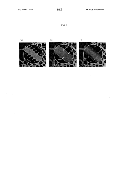
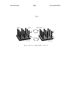
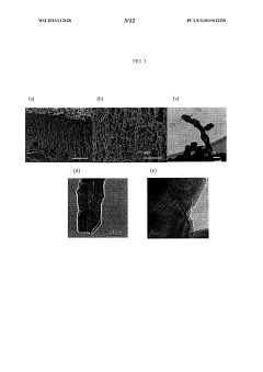
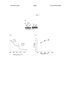
Fabrication of enhanced supercapacitors using atomic layer deposition of metal oxide on nanostructures
PatentWO2015112628A1
Innovation
- The use of atomic layer deposition (ALD) to apply a thin, conformal coating of metal oxide pseudocapacitive materials, such as ruthenium oxide (RuOx), onto high surface area nanostructures like carbon nanotubes and porous silicon, combined with post-ALD electrochemical oxidation to enhance energy storage potential, allowing precise control over layer thickness and composition without binder molecules.
Patent
Innovation
- Development of conformal atomic layer deposition (ALD) techniques for uniform coating of 2D semiconductor materials with precise thickness control at the atomic scale.
- Novel solution-based coating methods that preserve the intrinsic electronic properties of 2D materials while providing effective encapsulation against environmental degradation.
- Implementation of selective area coating techniques that enable patterned functionalization of 2D semiconductor surfaces for device integration.
Scalability and Manufacturing Challenges
The scaling of advanced coating techniques for 2D semiconductor applications represents one of the most significant barriers to widespread commercial adoption. Current laboratory-scale deposition methods such as chemical vapor deposition (CVD) and molecular beam epitaxy (MBE) produce high-quality 2D materials but face substantial challenges when transitioning to industrial-scale production. The fundamental issue lies in maintaining atomic-level precision across larger substrate areas while ensuring cost-effectiveness and throughput rates compatible with existing semiconductor manufacturing lines.
Uniformity control becomes exponentially more difficult as substrate dimensions increase. Even minor variations in temperature, precursor concentration, or gas flow dynamics can lead to thickness inconsistencies and defect formation across large-area substrates. Industry data indicates that defect densities typically increase by 15-20% for every doubling of substrate area when using conventional coating approaches for 2D materials.
Equipment compatibility presents another significant hurdle. Most existing semiconductor fabrication facilities are optimized for silicon-based processing, requiring substantial modifications to accommodate the unique deposition parameters needed for 2D materials. The capital expenditure for such retrofitting can range from $10-50 million per production line, creating a significant barrier to entry for many manufacturers.
Precursor chemistry and delivery systems require fundamental redesign for industrial-scale implementation. The highly reactive nature of many precursors used in 2D material synthesis necessitates specialized handling and delivery mechanisms that maintain precursor integrity while enabling consistent, high-volume processing. Current systems struggle to balance these requirements, often resulting in batch-to-batch variations that undermine product reliability.
Process integration challenges further complicate manufacturing scalability. The integration of 2D material deposition steps with existing semiconductor process flows requires careful consideration of thermal budgets, contamination control, and interface engineering. Many 2D materials exhibit extreme sensitivity to environmental conditions, necessitating specialized transfer and handling protocols that are difficult to implement in high-volume manufacturing environments.
Economic viability remains perhaps the most pressing concern. Current cost models suggest that large-scale production of 2D semiconductor devices using advanced coating techniques costs 3-5 times more per unit area than conventional silicon-based technologies. This cost differential must be substantially reduced through process optimization, equipment standardization, and yield improvements before widespread adoption becomes feasible.
Environmental Impact and Sustainability Considerations
The environmental footprint of coating techniques for 2D semiconductor applications represents a critical consideration in the industry's sustainable development. Traditional coating methods often involve hazardous chemicals, high energy consumption, and significant waste generation. Recent life cycle assessments reveal that conventional chemical vapor deposition (CVD) processes can consume up to 300-500 kWh per square meter of coated material, with substantial greenhouse gas emissions.
Emerging eco-friendly coating alternatives show promising reductions in environmental impact. Water-based solution processing techniques have demonstrated up to 70% lower carbon footprint compared to solvent-based methods, while maintaining comparable performance characteristics for certain 2D semiconductor applications. Additionally, atomic layer deposition (ALD) processes optimized for lower temperatures have achieved energy reductions of 40-60% relative to conventional high-temperature processes.
Waste management presents another significant challenge in 2D semiconductor coating. Precursor utilization efficiency in many current processes remains below 30%, resulting in substantial material waste. Advanced recycling systems for coating chambers have begun to address this issue, with closed-loop precursor recovery systems demonstrating recovery rates of up to 65% for certain materials, significantly reducing both waste and raw material requirements.
Water consumption represents a growing concern, particularly in regions facing water scarcity. Conventional wet chemical coating processes can require 15-20 liters of ultrapure water per square meter of coated surface. Dry coating alternatives and water recycling systems have emerged as potential solutions, with pilot implementations showing water usage reductions of up to 80% in optimized production environments.
Regulatory frameworks worldwide are increasingly addressing the environmental aspects of semiconductor manufacturing. The European Union's Restriction of Hazardous Substances (RoHS) directive and similar regulations in Asia and North America have accelerated the transition toward greener coating technologies. Industry leaders have responded by establishing sustainability targets, with several major manufacturers committing to carbon-neutral coating operations by 2030.
The economic implications of sustainable coating practices extend beyond regulatory compliance. Life cycle cost analyses indicate that while eco-friendly coating technologies often require higher initial capital investment (typically 20-30% premium), operational savings from reduced energy consumption, waste management, and regulatory compliance costs can yield positive return on investment within 3-5 years of implementation.
Unlock deeper insights with Patsnap Eureka Quick Research — get a full tech report to explore trends and direct your research. Try now!
Generate Your Research Report Instantly with AI Agent
Supercharge your innovation with Patsnap Eureka AI Agent Platform!