

2D Semiconductors in Emerging Aerospace Technologies
OCT 14, 202510 MIN READ
Generate Your Research Report Instantly with AI Agent
Patsnap Eureka helps you evaluate technical feasibility & market potential.
2D Semiconductors Background and Aerospace Applications
Two-dimensional (2D) semiconductors represent a revolutionary class of materials characterized by their atomic-scale thickness, typically consisting of one to few atomic layers. Since the groundbreaking isolation of graphene in 2004, the field has expanded to include transition metal dichalcogenides (TMDs) like MoS2 and WSe2, hexagonal boron nitride (h-BN), and other layered materials. These atomically thin semiconductors exhibit unique quantum confinement effects that dramatically alter their electronic, optical, and mechanical properties compared to their bulk counterparts.
The aerospace industry presents particularly demanding operational environments, requiring materials and components that can withstand extreme temperatures, radiation exposure, and mechanical stress while maintaining minimal weight. Traditional silicon-based semiconductors face significant limitations in these harsh conditions, creating a technological gap that 2D semiconductors are uniquely positioned to address.
2D semiconductors offer exceptional strength-to-weight ratios, with mechanical flexibility that enables integration into curved or complex aerospace structures. Their atomic thinness facilitates unprecedented miniaturization of electronic components, critical for reducing payload weight in spacecraft and aircraft systems. Many 2D materials demonstrate remarkable thermal stability and radiation hardiness, making them suitable candidates for space applications where conventional semiconductors would rapidly degrade.
In aerospace sensing applications, 2D materials exhibit extraordinary sensitivity to environmental changes. MoS2-based sensors can detect minute concentrations of gases relevant to cabin air quality monitoring and propulsion system diagnostics. The direct bandgap nature of many TMDs enables efficient light emission and absorption, supporting advanced optoelectronic systems for communication and navigation in aerospace platforms.
Power management represents another critical aerospace application. 2D semiconductor-based transistors demonstrate excellent switching characteristics and low power consumption, addressing the stringent energy efficiency requirements of spacecraft and satellite systems. Their potential for room-temperature operation reduces the need for cooling systems, further decreasing weight and power demands.
The radiation tolerance of certain 2D materials, particularly MoS2 and h-BN, offers significant advantages for long-duration space missions where cumulative radiation damage typically limits the operational lifespan of conventional electronics. Initial studies indicate that some 2D semiconductors can maintain functionality after radiation exposure levels that would render silicon-based devices inoperable.
Emerging aerospace applications include flexible avionics displays, ultra-lightweight solar cells for spacecraft power generation, and high-frequency communication systems capable of withstanding the extreme conditions of space. The integration of 2D semiconductors with traditional aerospace materials like carbon fiber composites is creating multifunctional structures that simultaneously provide structural support and electronic functionality.
Market Analysis for 2D Semiconductors in Aerospace
The global market for 2D semiconductors in aerospace applications is experiencing significant growth, driven by the unique properties these materials offer for extreme aerospace environments. Current market valuations indicate the 2D semiconductor sector for aerospace specifically reached approximately $450 million in 2022, with projections suggesting a compound annual growth rate of 24.3% through 2030, potentially reaching $2.1 billion by the end of the decade.
Demand is primarily concentrated in three aerospace subsectors: satellite communications, aircraft avionics, and space exploration systems. The satellite communications segment currently dominates with roughly 42% market share, as 2D semiconductor-based components offer significant advantages in reducing satellite weight while improving signal processing capabilities. This is particularly valuable as the small satellite constellation market continues its rapid expansion.
Regional analysis reveals North America leads with 38% of the global market share, followed by Europe at 29% and Asia-Pacific at 24%. The remaining 9% is distributed across other regions. The North American dominance stems from substantial aerospace defense budgets and the concentration of major aerospace manufacturers and research institutions in the region.
Key market drivers include the increasing miniaturization requirements for aerospace electronics, growing demand for radiation-hardened components, and the push for more fuel-efficient aircraft through weight reduction. The superior thermal management properties of 2D semiconductors address critical challenges in aerospace applications where traditional silicon-based semiconductors face performance limitations.
Market barriers include high production costs, with current manufacturing processes for aerospace-grade 2D semiconductors costing 4-6 times more than traditional semiconductors. Additionally, certification and qualification processes for aerospace components using novel materials typically require 3-5 years, creating significant market entry delays.
Customer segmentation shows defense contractors represent 47% of end-users, commercial aerospace manufacturers account for 31%, and space agencies comprise 22%. The remaining market consists of specialized research institutions and emerging private space companies.
Pricing trends indicate a gradual decrease of approximately 18% annually in production costs as manufacturing processes mature, though this remains insufficient to achieve price parity with traditional semiconductors in the near term. However, the performance benefits continue to justify the premium pricing for critical aerospace applications.
The competitive landscape is characterized by strategic partnerships between 2D semiconductor material suppliers and aerospace systems integrators, with vertical integration becoming increasingly common as companies seek to secure supply chains for these critical materials.
Current State and Challenges of 2D Semiconductors
The global landscape of 2D semiconductor research and development has witnessed remarkable progress in recent years, with significant advancements in material synthesis, characterization, and device fabrication. Currently, graphene remains the most extensively studied 2D material, followed by transition metal dichalcogenides (TMDs) such as MoS2, WS2, and WSe2. These materials have demonstrated exceptional electronic, optical, and mechanical properties that make them particularly attractive for aerospace applications.
In the United States, research institutions like MIT, Stanford, and national laboratories are leading efforts in developing high-performance 2D semiconductor devices for extreme environments. The European Union, through initiatives like the Graphene Flagship program, has established comprehensive research networks focused on translating 2D materials from laboratory to industrial applications. Meanwhile, China has significantly increased its research output and patent filings in this domain over the past five years, particularly in graphene-based technologies.
Despite promising progress, several critical challenges impede the widespread adoption of 2D semiconductors in aerospace technologies. The primary technical obstacle remains the scalable production of high-quality, defect-free 2D materials with consistent properties. Current synthesis methods like chemical vapor deposition (CVD) and mechanical exfoliation face limitations in producing large-area, uniform films required for practical aerospace applications.
Integration challenges present another significant hurdle. Incorporating 2D materials into conventional semiconductor manufacturing processes requires addressing issues of contamination, interface quality, and thermal management. The aerospace industry's stringent reliability requirements further complicate this integration, as devices must maintain performance under extreme conditions including radiation exposure, temperature fluctuations, and mechanical stress.
Stability and reliability concerns constitute a major constraint for aerospace implementation. Many 2D materials exhibit sensitivity to environmental factors such as oxygen and moisture, potentially compromising long-term performance in space environments. Additionally, the radiation hardness of 2D semiconductor devices remains insufficiently characterized for mission-critical aerospace applications.
The economic viability of 2D semiconductor technologies presents another challenge. Current production costs remain prohibitively high for mass deployment, with specialized equipment and expertise required throughout the manufacturing process. The aerospace industry's relatively small production volumes compared to consumer electronics further complicates the economic equation.
Standardization issues also persist across the field. The lack of universally accepted characterization methods, quality metrics, and performance benchmarks hinders meaningful comparison between different research efforts and slows industry adoption. This standardization gap is particularly problematic for aerospace applications, where rigorous qualification procedures are essential.
Current Implementation Solutions in Aerospace Systems
01 2D semiconductor materials and fabrication
Two-dimensional semiconductor materials have unique electronic properties due to their atomic-scale thickness. These materials include transition metal dichalcogenides, graphene derivatives, and other layered structures. Fabrication techniques involve exfoliation, chemical vapor deposition, and epitaxial growth methods to create atomically thin layers with controlled properties for electronic applications.- 2D semiconductor materials and fabrication methods: Two-dimensional semiconductor materials, such as transition metal dichalcogenides, graphene, and other atomically thin materials, have unique electronic properties that make them valuable for next-generation electronics. These materials exhibit exceptional carrier mobility, tunable bandgaps, and mechanical flexibility. Various fabrication methods including chemical vapor deposition, mechanical exfoliation, and epitaxial growth are used to produce high-quality 2D semiconductor layers with controlled thickness and composition.
- 2D semiconductor devices and applications: Two-dimensional semiconductors are being integrated into various electronic and optoelectronic devices including field-effect transistors, photodetectors, sensors, and memory devices. These materials enable the development of ultra-thin, flexible, and high-performance devices with improved electrical characteristics. Applications span from next-generation computing systems to wearable electronics, energy harvesting, and quantum information processing, leveraging the unique quantum confinement effects and surface-dominated properties of 2D materials.
- Heterostructures and interfaces of 2D semiconductors: Vertical stacking of different 2D materials creates heterostructures with novel electronic and optical properties not found in individual layers. These heterostructures enable band engineering, interlayer excitons, and enhanced carrier transport. The interfaces between 2D semiconductors and other materials (including 3D materials) play crucial roles in device performance, with research focusing on minimizing contact resistance, controlling band alignment, and engineering interface states to optimize electronic and optoelectronic properties.
- 2D semiconductor processing and integration technologies: Integration of 2D semiconductors into conventional semiconductor manufacturing processes presents unique challenges and opportunities. Specialized techniques for patterning, doping, contact formation, and encapsulation have been developed to preserve the intrinsic properties of 2D materials while enabling their incorporation into complex device architectures. Advanced processing methods include selective area growth, transfer printing, and laser-assisted processing to achieve precise control over material placement and interface quality.
- Quantum effects and modeling of 2D semiconductors: Two-dimensional semiconductors exhibit strong quantum confinement effects that significantly influence their electronic, optical, and thermal properties. Computational modeling and simulation techniques, including density functional theory, molecular dynamics, and quantum transport calculations, are essential for understanding and predicting the behavior of these materials at the atomic scale. These theoretical approaches guide experimental work by providing insights into electronic structure, defect behavior, and transport mechanisms in 2D semiconductor systems.
02 Device integration and architecture
Integration of 2D semiconductors into functional electronic devices requires specialized architectures and interface engineering. These include transistor structures, heterojunctions, and contact designs that leverage the unique properties of 2D materials. Novel device architectures enable improved performance in areas such as switching speed, power consumption, and form factor compared to conventional semiconductor devices.Expand Specific Solutions03 Optoelectronic applications
2D semiconductors exhibit exceptional optical properties that enable advanced optoelectronic applications. These materials feature direct bandgaps, strong light-matter interactions, and tunable optical responses. Applications include photodetectors, light-emitting devices, photovoltaics, and optical sensors with enhanced sensitivity, flexibility, and integration capabilities.Expand Specific Solutions04 Quantum and electronic properties
The quantum confinement effects in 2D semiconductors lead to unique electronic properties that can be exploited for next-generation computing and information processing. These materials exhibit phenomena such as valley polarization, spin-orbit coupling, and quantum confinement that enable novel electronic functionalities. Research focuses on understanding and controlling these quantum properties for applications in quantum computing, spintronics, and valleytronics.Expand Specific Solutions05 Heterostructures and composite materials
Combining different 2D semiconductors into heterostructures or with other materials creates composite systems with enhanced or novel properties. These engineered structures enable band alignment engineering, interlayer coupling effects, and multifunctional capabilities. Applications include high-performance electronics, sensors, energy storage, and conversion devices that benefit from the synergistic properties of the constituent materials.Expand Specific Solutions
Key Industry Players and Research Institutions
The 2D semiconductor market in aerospace technologies is in an early growth phase, characterized by significant R&D investment and emerging commercial applications. The global market is projected to expand rapidly, driven by demands for lightweight, energy-efficient components in next-generation aerospace systems. While technology maturity varies across applications, leading players are advancing the field at different rates. TSMC and Samsung are establishing manufacturing capabilities, while academic institutions like MIT, Manchester University, and Tsinghua University are pioneering fundamental research. Companies including Huawei, IBM, and Micron are developing specialized applications, with GlobalFoundries and Canon focusing on integration with existing semiconductor technologies. This competitive landscape reflects a strategic race to commercialize 2D semiconductor solutions for the unique requirements of aerospace environments.
Taiwan Semiconductor Manufacturing Co., Ltd.
Technical Solution: TSMC has developed advanced fabrication processes specifically for 2D semiconductor materials targeting aerospace applications. Their approach centers on integrating atomically thin materials like MoS2 and WSe2 with their established semiconductor manufacturing infrastructure. TSMC has created specialized deposition systems that can produce uniform 2D material layers across 300mm wafers with industry-leading consistency[5]. Their technology includes proprietary contact engineering methods that overcome the traditional challenges of forming low-resistance electrical connections to 2D materials. For aerospace applications, TSMC has developed radiation-hardened design libraries specifically for 2D semiconductor devices, enabling system designers to create space-qualified circuits using their process technology. They've also pioneered specialized packaging solutions that protect delicate 2D materials while maintaining their flexibility and weight advantages. TSMC's manufacturing approach includes rigorous quality control protocols specifically adapted for the unique challenges of 2D materials, ensuring reliability standards compatible with aerospace requirements[7].
Strengths: TSMC brings unparalleled manufacturing expertise and established quality control systems to 2D semiconductor production, with the capacity to scale production to meet aerospace industry demands. Their established supply chain relationships facilitate integration into existing aerospace systems. Weaknesses: As primarily a contract manufacturer, TSMC depends on designs from customers and partners, potentially limiting their ability to drive innovation independently. Their processes are optimized for traditional silicon, requiring significant adaptation for 2D materials.
Samsung Electronics Co., Ltd.
Technical Solution: Samsung has developed comprehensive 2D semiconductor solutions targeting next-generation aerospace electronics. Their approach leverages transition metal dichalcogenides (TMDs) and graphene derivatives to create ultra-lightweight, flexible electronic components that maintain functionality in extreme space environments. Samsung's technology includes specialized synthesis methods that produce high-quality 2D materials at scales compatible with their established semiconductor manufacturing infrastructure[9]. They've created radiation-hardened memory devices using 2D materials that demonstrate exceptional resistance to single-event upsets caused by cosmic radiation, a critical requirement for space applications. Samsung has pioneered flexible display and sensor technologies using 2D semiconductors that can be integrated into curved surfaces of aerospace vehicles without compromising performance. Their research includes specialized interface engineering techniques that optimize connections between 2D materials and conventional electronics, ensuring reliable signal transmission in aerospace systems. Samsung has also developed energy-efficient computing architectures using 2D semiconductors that significantly reduce power consumption while maintaining processing capabilities needed for autonomous aerospace operations[10].
Strengths: Samsung brings extensive manufacturing infrastructure and supply chain integration capabilities, allowing for potential mass production of 2D semiconductor devices. Their diverse technology portfolio enables comprehensive system solutions rather than just individual components. Weaknesses: Their aerospace-specific experience is more limited compared to dedicated aerospace suppliers, potentially requiring partnerships to navigate certification requirements. The technology remains at relatively early stages of commercialization for aerospace applications.
Critical Patents and Research Breakthroughs
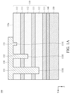
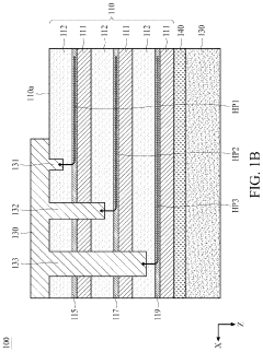
Semiconductor device with multichannel heterostructure and manufacturing method thereof
PatentActiveUS20220140094A1
Innovation
- A semiconductor device with a multichannel heterostructure is developed, featuring alternating semiconductor material layers with conductive fingers that progressively increase or decrease in length to avoid contact with two-dimensional hole gases (2DHGs), allowing for efficient electron hole flow and dispersion through the formation of multiple channels.
Thermally activated memristors, fabricating methods and applications of same
PatentActiveUS10944047B2
Innovation
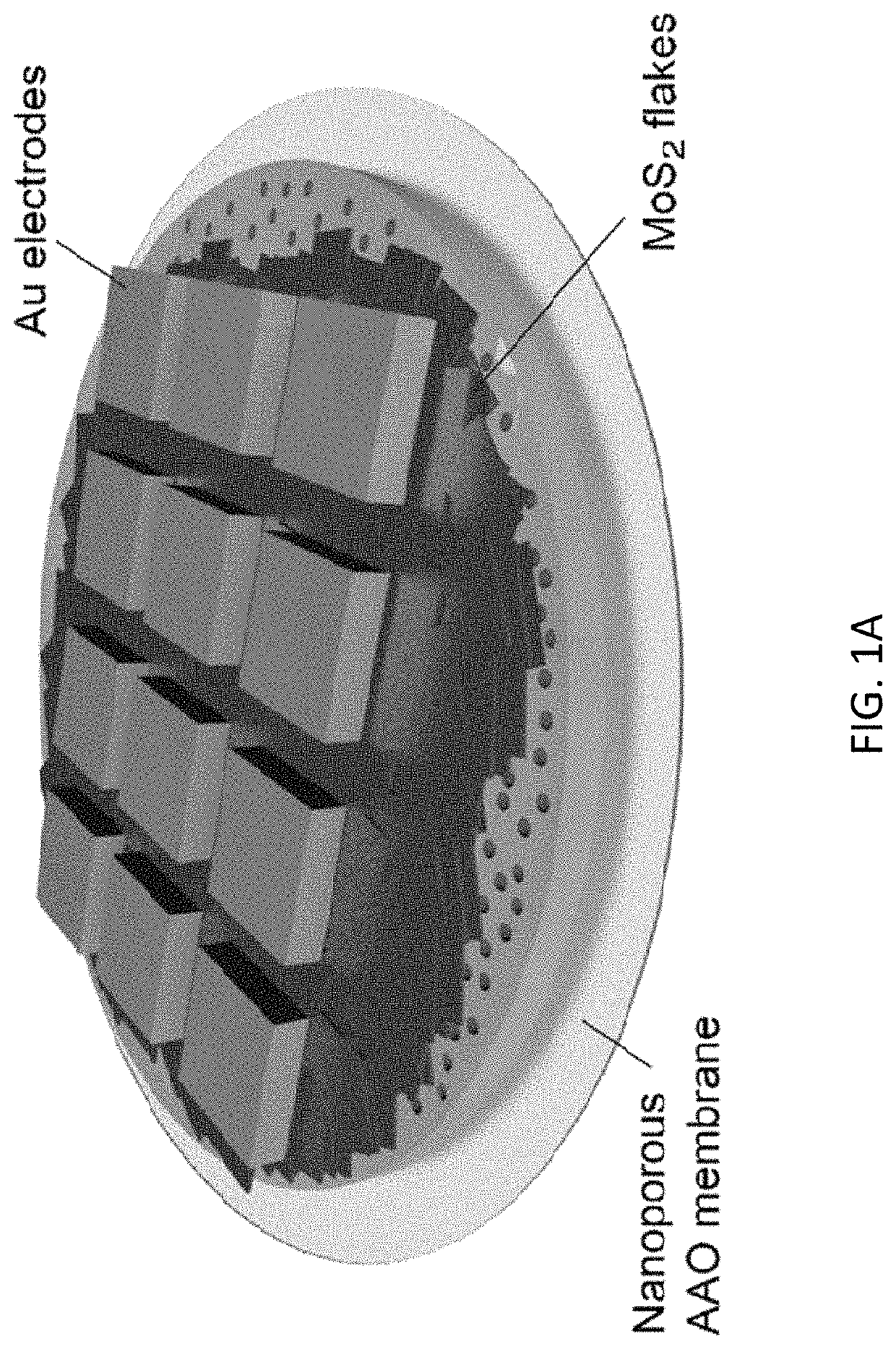
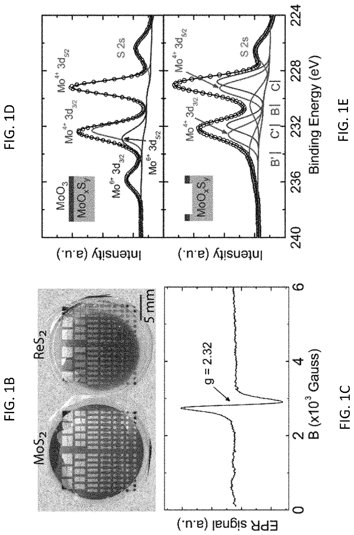
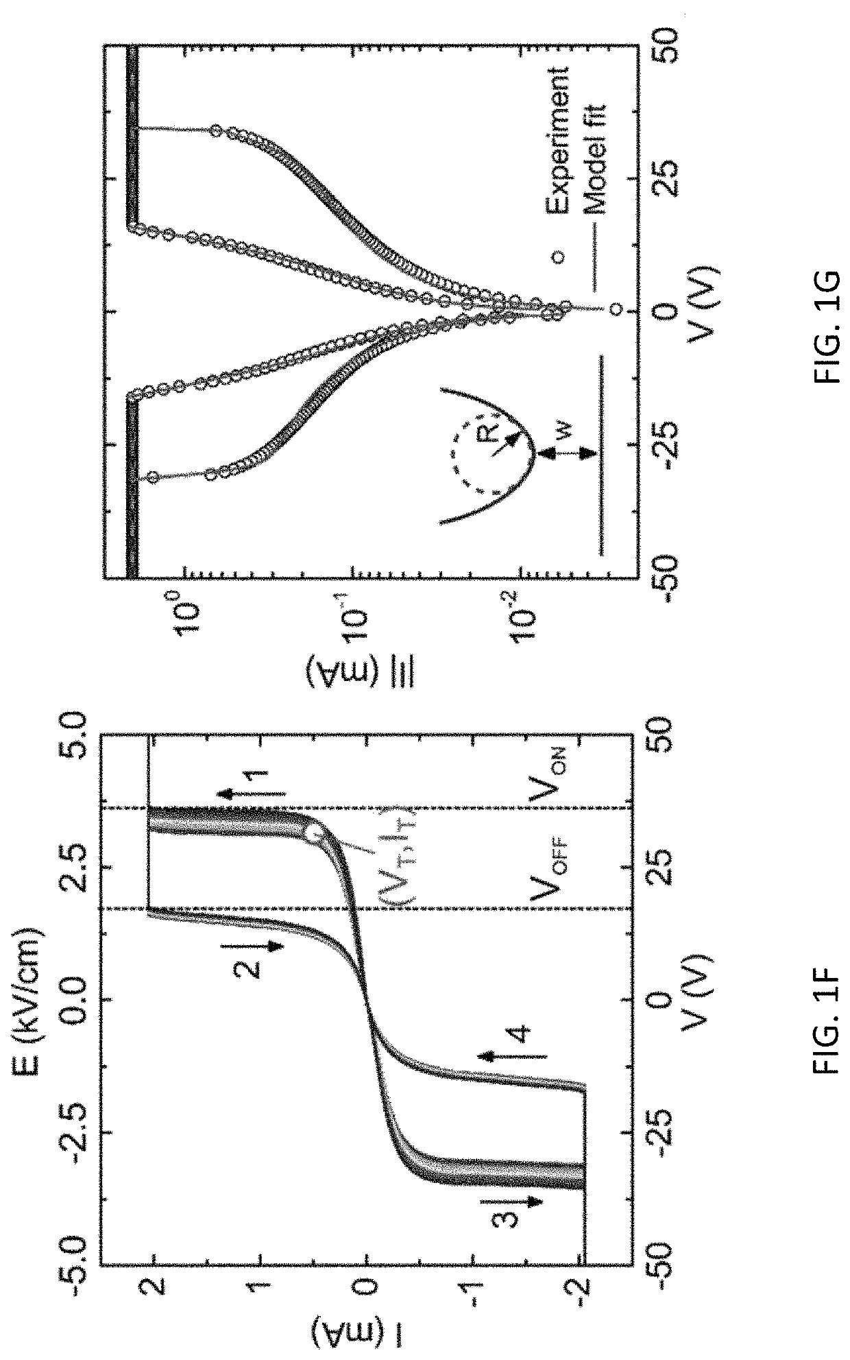
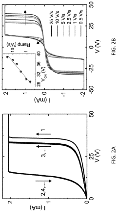
- Thermally activated memristors are fabricated from composite films of solution-processed two-dimensional semiconductors, featuring switching behavior driven by thermally activated electrical discharge between nanosized flakes, allowing for scalable and reproducible manufacturing with excellent stability, and can act as soft or hard thermistors or WORM memory depending on thickness.
Space Environment Reliability and Radiation Hardening
The space environment presents unique challenges for electronic components due to extreme conditions including vacuum, temperature fluctuations, and most critically, radiation exposure. 2D semiconductors demonstrate promising characteristics for aerospace applications, but their reliability in such harsh environments requires thorough evaluation. Initial studies indicate that certain 2D materials, particularly transition metal dichalcogenides (TMDs) like MoS2 and WSe2, exhibit inherent radiation hardness superior to traditional silicon-based semiconductors.
Radiation effects in space can be categorized into Total Ionizing Dose (TID), Single Event Effects (SEEs), and displacement damage. 2D semiconductors show remarkable resilience against TID effects due to their atomically thin nature, which reduces the volume available for charge trapping. Research conducted by NASA and the European Space Agency demonstrates that MoS2-based field-effect transistors maintain operational stability after exposure to gamma radiation doses exceeding 10 Mrad, significantly outperforming conventional silicon technologies.
For SEEs, which result from high-energy particle strikes, 2D materials benefit from reduced charge collection volumes. The ultrathin channel regions in 2D semiconductor devices minimize the cross-section for particle interactions, potentially reducing the occurrence of transient upsets and latchups. However, substrate interactions remain a concern, as secondary particles generated in underlying materials can still induce failures in 2D device structures.
Temperature stability represents another critical aspect of space reliability. The wide bandgap nature of many 2D semiconductors enables operation across broader temperature ranges than silicon. Hexagonal boron nitride (h-BN) encapsulation techniques have proven effective in enhancing the thermal stability of 2D electronic systems, maintaining performance integrity from -150°C to +150°C, encompassing the typical thermal cycling experienced in orbit.
Radiation hardening approaches for 2D semiconductor technologies include both intrinsic and extrinsic strategies. Intrinsically, the selection of specific 2D materials with stronger atomic bonds and defect-resistant structures enhances radiation tolerance. Extrinsically, novel device architectures incorporating radiation-resistant gate dielectrics (such as hafnium oxide) and specialized encapsulation layers provide additional protection.
Recent advancements in heterostructure engineering, where multiple 2D materials are stacked with atomic precision, offer promising pathways for creating radiation-hardened systems. These engineered structures can incorporate sacrificial layers designed to absorb radiation damage while preserving the functionality of critical device components. Preliminary testing on MoS2/h-BN/graphene heterostructures demonstrates functionality retention after proton irradiation at doses equivalent to decades in low Earth orbit.
Supply Chain Security and Material Sourcing Strategies
The aerospace industry's adoption of 2D semiconductors faces unique supply chain challenges that require strategic approaches to material sourcing. Currently, the supply chain for critical 2D materials such as graphene, molybdenum disulfide, and hexagonal boron nitride remains highly concentrated in specific geographic regions, creating significant vulnerabilities. China dominates the production of rare earth elements essential for these advanced materials, while the United States and Europe maintain technological advantages in processing and device fabrication.
Supply chain disruptions during the COVID-19 pandemic revealed critical weaknesses in the aerospace sector's ability to source these specialized materials. The highly specialized nature of 2D semiconductor materials, combined with limited supplier diversity, has created bottlenecks that threaten production continuity for aerospace applications. These vulnerabilities are particularly concerning given the strategic importance of aerospace technologies to national security and defense capabilities.
To address these challenges, leading aerospace manufacturers are implementing multi-sourcing strategies that diversify their supplier networks across different geographic regions. Companies like Lockheed Martin and Boeing have established partnerships with materials science companies in North America, Europe, and select Asian countries to ensure redundancy in their supply chains. These partnerships often include co-development agreements that help stabilize material availability while advancing technical capabilities.
Vertical integration has emerged as another key strategy, with major aerospace corporations acquiring or developing in-house capabilities for critical material production. This approach reduces dependency on external suppliers while providing greater quality control over specialized 2D semiconductor materials. Raytheon Technologies, for example, has invested in proprietary synthesis processes for hexagonal boron nitride, a critical component in high-temperature aerospace electronics.
Stockpiling of essential materials represents a short-term risk mitigation strategy, though this approach faces limitations due to the shelf life of certain precursor chemicals and the rapid pace of material innovation. More sustainable approaches include the development of material recycling and reclamation processes specific to 2D semiconductors, which are beginning to show promise in laboratory settings but require further scaling for industrial implementation.
International cooperation frameworks are also evolving to address supply chain security. The Aerospace Materials Consortium, formed in 2022, brings together industry leaders, academic institutions, and government agencies to coordinate research efforts and establish material standards. These collaborative initiatives aim to create more resilient supply networks while accelerating the commercialization of alternative material sources and synthesis methods.
Unlock deeper insights with Patsnap Eureka Quick Research — get a full tech report to explore trends and direct your research. Try now!
Generate Your Research Report Instantly with AI Agent
Supercharge your innovation with Patsnap Eureka AI Agent Platform!