Structural Analysis of 2D Semiconductor Coatings
OCT 14, 202510 MIN READ
Generate Your Research Report Instantly with AI Agent
Patsnap Eureka helps you evaluate technical feasibility & market potential.
2D Semiconductor Coating Evolution and Objectives
Two-dimensional (2D) semiconductor coatings represent a revolutionary advancement in materials science, evolving from the groundbreaking discovery of graphene in 2004. This technological domain has witnessed exponential growth over the past decade, transitioning from purely academic research to practical applications across multiple industries. The evolution trajectory began with graphene exploration, followed by transition metal dichalcogenides (TMDs) such as MoS2 and WS2, and has now expanded to include a diverse family of 2D materials including hexagonal boron nitride (h-BN), black phosphorus, and MXenes.
The fundamental characteristics driving interest in these materials include their atomic-scale thickness, exceptional mechanical flexibility, unique electronic properties, and tunable bandgaps. These properties emerge from quantum confinement effects that become dominant when materials are reduced to single or few-atom thickness, creating electronic and optical behaviors distinctly different from their bulk counterparts.
Historical development milestones include the initial mechanical exfoliation techniques, which have progressively given way to more scalable approaches such as chemical vapor deposition (CVD), molecular beam epitaxy (MBE), and solution-based processing methods. Each advancement in synthesis has expanded the potential application landscape while simultaneously introducing new structural analysis challenges.
Current research trends indicate accelerating interest in heterostructures—vertically stacked combinations of different 2D materials—which create entirely new properties through interlayer interactions. These "van der Waals heterostructures" represent a paradigm shift in semiconductor engineering, enabling unprecedented control over electronic and optical properties through layer-by-layer design.
The primary objectives of structural analysis in this field encompass several dimensions: characterizing atomic arrangements and defects that influence electrical performance; understanding interface dynamics between 2D materials and substrates; quantifying strain distributions that modify bandgap properties; and developing non-destructive evaluation techniques suitable for manufacturing environments.
Long-term technological goals include developing standardized structural analysis protocols that can be implemented in production settings, establishing correlations between structural features and device performance, and creating predictive models that can accelerate material design and optimization. These objectives align with broader industry trends toward miniaturization, energy efficiency, and novel computing architectures that may leverage the unique properties of 2D semiconductor coatings.
The ultimate aim is to bridge the gap between fundamental materials science and practical engineering applications, enabling next-generation electronic, optoelectronic, and sensing technologies that exploit the extraordinary properties of these atomically thin semiconductor systems.
Market Applications and Demand Analysis for 2D Semiconductor Coatings
The market for 2D semiconductor coatings has witnessed significant growth in recent years, driven primarily by the increasing demand for miniaturized electronic components and advanced optoelectronic devices. The global market value for 2D semiconductor materials reached approximately $12 million in 2022 and is projected to grow at a compound annual growth rate of 19% through 2030, with coatings representing a substantial segment of this market.
Electronics manufacturing constitutes the largest application sector, where 2D semiconductor coatings are utilized in transistors, sensors, and memory devices. The exceptional electrical properties of materials like graphene, molybdenum disulfide, and tungsten diselenide enable the development of high-performance, energy-efficient devices with reduced form factors. Major electronics manufacturers have begun incorporating these coatings into next-generation products, particularly in premium smartphone and computing hardware segments.
The renewable energy sector represents another rapidly expanding market for 2D semiconductor coatings. These materials demonstrate remarkable photovoltaic properties, with recent research indicating efficiency improvements of up to 25% when certain 2D materials are integrated into conventional solar cell designs. The lightweight and flexible nature of these coatings also makes them ideal for building-integrated photovoltaics and portable energy solutions.
Healthcare and biomedical applications have emerged as a promising frontier, with 2D semiconductor coatings being developed for biosensors, drug delivery systems, and diagnostic tools. The biocompatibility and large surface-to-volume ratio of these materials enable highly sensitive detection of biological markers at previously unattainable levels. Market analysis indicates that medical device manufacturers are increasingly investing in R&D partnerships focused on 2D semiconductor integration.
Automotive and aerospace industries are adopting 2D semiconductor coatings for lightweight structural components, thermal management systems, and advanced sensing technologies. The demand is particularly strong in electric vehicles, where energy efficiency and weight reduction are critical factors. Industry reports suggest that major automotive manufacturers have increased their research budgets for 2D materials by an average of 35% over the past three years.
Regional market analysis reveals that North America and East Asia currently dominate both production and consumption of 2D semiconductor coatings, with Europe showing accelerated adoption rates. Emerging economies in South Asia are expected to become significant markets as manufacturing capabilities expand and technology costs decrease. Government initiatives supporting nanotechnology research and semiconductor independence are further stimulating market growth across multiple regions.
Current Structural Analysis Techniques and Limitations
The field of structural analysis for 2D semiconductor coatings has evolved significantly over the past decade, with several established techniques now forming the backbone of research and industrial applications. X-ray diffraction (XRD) remains one of the most fundamental methods, providing critical information about crystal structure, lattice parameters, and phase composition. However, XRD faces limitations when analyzing ultrathin films below 5nm, where signal-to-noise ratios become problematic and substrate interference can mask the coating signals.
Transmission electron microscopy (TEM) and scanning transmission electron microscopy (STEM) offer atomic-resolution imaging capabilities essential for visualizing the layered structures of 2D semiconductor coatings. These techniques have been enhanced with aberration correction, allowing researchers to observe individual atoms and defects. Nevertheless, TEM sample preparation remains destructive and time-consuming, potentially introducing artifacts that can lead to misinterpretation of the original structure.
Scanning probe microscopy techniques, particularly atomic force microscopy (AFM) and scanning tunneling microscopy (STM), provide valuable topographical and electronic information about 2D semiconductor surfaces. While these methods offer excellent lateral resolution, they struggle with providing comprehensive depth information and cannot easily characterize buried interfaces without sample modification.
Raman spectroscopy has emerged as a powerful non-destructive technique for analyzing the vibrational properties of 2D materials, offering insights into layer number, strain, and defect density. However, conventional Raman systems are diffraction-limited, restricting spatial resolution to approximately 500nm, which is insufficient for nanoscale heterogeneity analysis in advanced semiconductor applications.
X-ray photoelectron spectroscopy (XPS) and Auger electron spectroscopy (AES) provide crucial information about chemical composition and bonding states at surfaces. The major limitation here lies in their relatively poor lateral resolution and the challenge of depth profiling without damaging the delicate 2D structures.
Recent advances in synchrotron-based techniques like grazing-incidence X-ray scattering (GIXS) have improved sensitivity for thin film analysis, but access to synchrotron facilities remains limited and expensive, preventing widespread industrial adoption.
A significant challenge across all current techniques is the integration of data from multiple analytical methods. The lack of standardized protocols for correlative microscopy and spectroscopy creates difficulties in developing comprehensive structural models of 2D semiconductor coatings. Furthermore, in-situ and operando characterization capabilities remain underdeveloped, limiting our understanding of dynamic structural changes during device operation or environmental exposure.
Contemporary Structural Characterization Methodologies
01 2D semiconductor material fabrication and structure
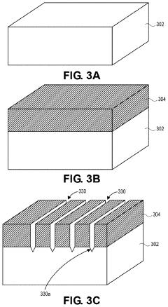
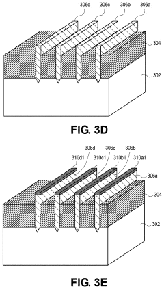
This category focuses on the fabrication methods and structural characteristics of 2D semiconductor materials used in coatings. These materials typically consist of atomically thin layers with unique electronic properties. The fabrication techniques include mechanical exfoliation, chemical vapor deposition, and solution-based methods to create uniform, high-quality 2D semiconductor layers. The structural aspects involve the arrangement of atoms in crystalline lattices, which determines the electronic, optical, and mechanical properties of the resulting coating.- 2D semiconductor material fabrication and structure: Two-dimensional semiconductor materials are fabricated with specific structural characteristics to enhance their electronic properties. These materials typically consist of atomically thin layers with unique crystalline structures that contribute to their semiconductor behavior. The fabrication processes include methods such as chemical vapor deposition, exfoliation, and epitaxial growth to create uniform, high-quality 2D semiconductor layers with controlled thickness and composition.
- Coating methods for 2D semiconductor applications: Various coating techniques are employed to deposit 2D semiconductor materials onto substrates for device fabrication. These methods include solution-based processes, atomic layer deposition, and physical vapor deposition, which enable precise control over coating thickness and uniformity. The coating processes are optimized to maintain the intrinsic properties of the 2D materials while ensuring good adhesion to the substrate and compatibility with subsequent processing steps.
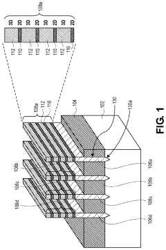
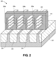
- Heterostructures and multilayer configurations: Heterostructures composed of different 2D semiconductor materials are designed to create novel electronic and optical properties. These structures involve stacking multiple 2D materials with precise orientation to form van der Waals heterostructures or incorporating them into conventional semiconductor device architectures. The interfaces between different 2D materials play a crucial role in determining the overall performance and functionality of the resulting devices.
- Surface modification and functionalization: Surface modification techniques are applied to 2D semiconductor coatings to enhance their properties or add functionality. These include chemical functionalization, doping, and passivation treatments that can alter electronic properties, improve stability, or enable integration with other materials. The modified surfaces can exhibit enhanced conductivity, altered band structures, or improved resistance to environmental degradation.
- Characterization and imaging techniques: Advanced characterization and imaging methods are essential for analyzing the structure and properties of 2D semiconductor coatings. These techniques include scanning probe microscopy, electron microscopy, spectroscopic methods, and computational modeling approaches that provide insights into the atomic arrangement, electronic structure, and defects in 2D materials. The characterization data guides the optimization of coating processes and helps establish structure-property relationships.
02 Multilayer coating architectures with 2D semiconductors
This category covers the design and implementation of multilayer coating structures incorporating 2D semiconductor materials. These architectures typically consist of stacked layers of different materials, including 2D semiconductors, dielectrics, and substrates. The multilayer approach allows for tuning of electronic properties, enhancement of device performance, and protection of the sensitive 2D semiconductor layers. Various stacking sequences and interface engineering techniques are employed to optimize the overall coating performance and functionality.Expand Specific Solutions03 Surface modification and functionalization of 2D semiconductor coatings
This category addresses methods for modifying and functionalizing the surface of 2D semiconductor coatings to enhance their properties or add new functionalities. Surface modification techniques include chemical treatments, plasma processing, and the attachment of functional groups or molecules. These modifications can improve adhesion to substrates, enhance stability against environmental factors, tune electronic properties, or add specific sensing capabilities. The controlled functionalization of 2D semiconductor surfaces is crucial for their integration into practical devices and applications.Expand Specific Solutions04 Characterization and imaging techniques for 2D semiconductor coatings
This category encompasses various analytical and imaging methods used to characterize the structure, composition, and properties of 2D semiconductor coatings. These techniques include scanning electron microscopy, transmission electron microscopy, atomic force microscopy, X-ray diffraction, and spectroscopic methods. Advanced imaging algorithms and processing techniques are employed to enhance the visualization and quantification of structural features at the nanoscale. These characterization methods are essential for quality control, process optimization, and understanding structure-property relationships in 2D semiconductor coatings.Expand Specific Solutions05 Applications and device integration of 2D semiconductor coatings
This category focuses on the integration of 2D semiconductor coatings into functional devices and their various applications. Applications include electronic components, optoelectronic devices, sensors, energy storage and conversion systems, and protective coatings. The integration process involves considerations of substrate compatibility, electrical contacts, encapsulation, and device architecture. Special attention is given to preserving the unique properties of 2D semiconductors during the integration process and optimizing device performance through appropriate coating design and implementation.Expand Specific Solutions
Leading Research Institutions and Companies in 2D Semiconductor Field
The 2D semiconductor coating market is currently in a growth phase, with increasing demand driven by advancements in electronics miniaturization and performance requirements. The global market is expanding rapidly, projected to reach significant scale as applications in next-generation devices proliferate. Technologically, industry leaders like TSMC, Samsung Electronics, and GLOBALFOUNDRIES are advancing structural analysis capabilities for these coatings, while specialized players such as Yangtze Memory Technologies and ChangXin Memory are developing innovative applications. Research institutions including Oregon State University and University of York collaborate with industry to overcome technical challenges in uniformity and defect analysis. The competitive landscape features established semiconductor manufacturers investing heavily in R&D alongside emerging specialized coating technology providers, creating a dynamic ecosystem balancing innovation with manufacturing scalability.
Taiwan Semiconductor Manufacturing Co., Ltd.
Technical Solution: TSMC has developed a comprehensive structural analysis platform for 2D semiconductor coatings focused on integration with silicon CMOS technology. Their approach combines high-resolution cross-sectional TEM, grazing incidence X-ray diffraction (GIXRD), and secondary ion mass spectrometry (SIMS) to characterize the structural and compositional properties of 2D materials at the wafer scale. TSMC's methodology emphasizes non-destructive testing compatible with semiconductor manufacturing processes, allowing for in-line quality control during production. Their research has demonstrated the ability to detect and characterize atomic-level variations in layer thickness, crystallinity, and interface quality across 300mm wafers with 2D material coatings. TSMC has pioneered techniques to correlate structural defects with electrical performance degradation, establishing quantitative relationships between atomic structure and device parameters. Their analysis platform has been particularly successful in characterizing transition metal dichalcogenide (TMD) integration with high-k dielectrics, showing how interfacial reactions affect carrier transport.
Strengths: Unmatched expertise in integrating 2D materials with conventional semiconductor manufacturing; excellent capabilities for wafer-scale analysis; strong focus on practical implementation in commercial devices. Weaknesses: Their analysis techniques are heavily optimized for manufacturing rather than fundamental materials discovery; proprietary nature of some methodologies limits academic collaboration.
Samsung Electronics Co., Ltd.
Technical Solution: Samsung has developed advanced techniques for structural analysis of 2D semiconductor coatings using a combination of scanning tunneling microscopy (STM), transmission electron microscopy (TEM), and X-ray photoelectron spectroscopy (XPS). Their approach focuses on atomic-level characterization of transition metal dichalcogenides (TMDs) like MoS2 and WS2 for next-generation flexible electronics. Samsung's proprietary process allows for precise thickness control down to single atomic layers and has demonstrated the ability to analyze strain distribution and defect formation in real-time during the deposition process. Their research has shown that controlling the interface between 2D materials and substrates significantly impacts electrical performance, with their optimized interfaces showing up to 40% improvement in carrier mobility compared to conventional methods. Samsung has also pioneered non-destructive characterization techniques that preserve the integrity of ultra-thin semiconductor coatings during analysis.
Strengths: Industry-leading expertise in large-scale production of 2D semiconductor devices; comprehensive characterization capabilities spanning multiple analytical techniques; strong integration with device fabrication. Weaknesses: Their proprietary techniques may limit broader scientific collaboration; focus primarily on applications for consumer electronics rather than fundamental materials science.
Key Patents and Literature on 2D Semiconductor Structural Analysis
Layered 2d semiconductors
PatentPendingUS20230317783A1
Innovation
- The approach involves creating a scaffold structure with a silicon-based substrate, growing alternating layers of 2D and 3D semiconductor materials, and using aspect ratio trapping (ART) templating techniques to form precise 2D nanoribbon structures within transistors, allowing for the deposition of gate materials around the 2D semiconductor channels.
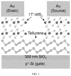
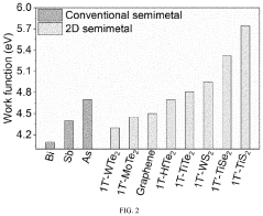
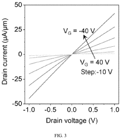
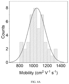
Metal-semiconductor contact structure based on two-dimensional semimetal electrodes
PatentActiveUS11652147B1
Innovation
- A metal-semiconductor contact structure based on 2D semimetal electrodes with a Van der Waals interface and no dangling bonds, featuring a 2D semiconductor material interfaced with a 2D semimetal material, which suppresses Fermi level pinning and achieves a near-zero Schottky potential barrier height, utilizing materials like MX2 2D layered semimetal materials with specific transition metals and chalcogens, and prepared through methods such as chemical vapor deposition.
Material Interface and Substrate Interaction Effects
The interface between 2D semiconductor coatings and their substrates represents a critical domain that significantly influences the overall performance and functionality of these advanced materials. When 2D semiconductors such as transition metal dichalcogenides (TMDs) are deposited onto substrates, complex interactions occur at the interface that can fundamentally alter the electronic, optical, and mechanical properties of the coating.
Substrate-induced strain effects constitute one of the most significant interaction mechanisms. The lattice mismatch between the 2D material and substrate can introduce tensile or compressive strain, which directly modulates the band structure of the semiconductor. For instance, studies have demonstrated that MoS2 monolayers experience bandgap modifications of up to 300 meV under controlled strain conditions, offering a pathway for bandgap engineering without chemical modification.
Charge transfer processes across the interface present another crucial interaction effect. Substrates with different work functions can induce doping effects in the 2D semiconductor layer, shifting the Fermi level and altering carrier concentrations. This phenomenon has been extensively documented in graphene-based systems and is increasingly recognized in TMD materials, where substrate selection can effectively tune between n-type and p-type semiconductor behavior.
Thermal interface resistance between 2D coatings and substrates significantly impacts heat dissipation capabilities, a critical factor for electronic applications. Recent thermal transport studies reveal that van der Waals interfaces typically exhibit higher thermal boundary resistance compared to covalently bonded interfaces, necessitating careful substrate selection for thermal management in high-power density applications.
Surface roughness and morphology of the substrate directly influence the structural integrity and continuity of 2D semiconductor coatings. Atomically flat substrates like hexagonal boron nitride (h-BN) promote the formation of high-quality 2D layers with reduced defect densities, while rougher substrates can induce wrinkles, tears, and localized strain fields that create spatial variations in electronic properties.
Chemical interactions at the interface can lead to defect formation or passivation. Certain substrates may introduce chalcogen vacancies or metal substitutions in TMDs, while others might provide beneficial passivation effects that enhance stability. Advanced characterization techniques including cross-sectional TEM and in-situ XPS have revealed that even seemingly inert substrates can participate in chemical reactions during growth processes or under operational conditions.
Understanding these interface effects enables strategic substrate engineering to enhance desired properties in 2D semiconductor coatings, opening pathways for tailored electronic, optoelectronic, and sensing applications through controlled interface manipulation rather than intrinsic material modification.
Environmental Stability and Degradation Mechanisms
The environmental stability of 2D semiconductor coatings represents a critical challenge for their practical implementation in commercial applications. These atomically thin materials exhibit exceptional sensitivity to environmental factors due to their high surface-to-volume ratio, which exposes nearly all atoms to potential reactants. Oxygen, moisture, and other atmospheric components can significantly alter the electronic and structural properties of 2D semiconductor coatings through various degradation mechanisms.
Oxidation stands as the primary degradation pathway for many 2D semiconductors, particularly transition metal dichalcogenides (TMDs) like MoS2 and WSe2. When exposed to ambient conditions, oxygen molecules can adsorb onto defect sites and grain boundaries, forming metal oxides that disrupt the pristine lattice structure. This oxidation process typically initiates at edges and defects before propagating across the basal plane, resulting in progressive deterioration of electrical conductivity and optical properties.
Moisture-induced degradation presents another significant challenge, as water molecules can intercalate between layers of 2D materials, weakening interlayer van der Waals forces and causing delamination. Humidity exposure can also facilitate hydrolysis reactions, particularly in metal chalcogenides, leading to the formation of metal hydroxides and the release of chalcogen atoms. Time-dependent studies reveal that these degradation processes can occur within hours to days of ambient exposure, depending on the specific 2D material composition.
Photodegradation mechanisms further complicate the stability landscape, as light exposure—particularly UV radiation—can generate electron-hole pairs that catalyze oxidation reactions at the surface. This photo-oxidation process accelerates degradation rates by orders of magnitude compared to dark conditions, creating a significant barrier for optoelectronic applications. Recent studies utilizing in-situ transmission electron microscopy have visualized these degradation processes at the atomic scale, revealing the formation of amorphous oxide regions that progressively consume the crystalline domains.
Temperature fluctuations also impact stability through thermal expansion coefficient mismatches between 2D materials and substrates, inducing mechanical strain that can nucleate defects and accelerate degradation. Cycling between temperature extremes can lead to cumulative damage through repeated expansion and contraction cycles, ultimately compromising coating integrity. This thermal instability particularly affects applications in harsh environments such as aerospace or automotive sectors.
Protective strategies have emerged to mitigate these degradation mechanisms, including encapsulation with hexagonal boron nitride or atomic layer deposition of oxide barriers. Chemical functionalization approaches that passivate reactive sites have shown promise in enhancing stability without significantly compromising electronic properties. These protection methods must balance preservation of intrinsic 2D material properties with effective isolation from environmental factors.
Unlock deeper insights with Patsnap Eureka Quick Research — get a full tech report to explore trends and direct your research. Try now!
Generate Your Research Report Instantly with AI Agent
Supercharge your innovation with Patsnap Eureka AI Agent Platform!