

Unveiling 2D Semiconductor Properties in Electronics
OCT 14, 20259 MIN READ
Generate Your Research Report Instantly with AI Agent
Patsnap Eureka helps you evaluate technical feasibility & market potential.
2D Semiconductor Evolution and Research Objectives
Two-dimensional (2D) semiconductors have emerged as a revolutionary class of materials in the field of electronics, representing a significant departure from traditional three-dimensional semiconductor technologies. Since the groundbreaking isolation of graphene in 2004, the exploration of 2D materials has expanded dramatically, encompassing transition metal dichalcogenides (TMDs), hexagonal boron nitride (h-BN), and various other atomically thin structures. This evolution marks a paradigm shift in semiconductor physics and engineering, driven by the unique properties that manifest when materials are confined to the atomic scale.
The historical trajectory of 2D semiconductor development can be traced through several key milestones. Following graphene's discovery, researchers identified semiconducting behavior in molybdenum disulfide (MoS2) and other TMDs around 2010, catalyzing intensive research into their electronic properties. By 2015, the field had progressed to creating heterostructures—layered combinations of different 2D materials—enabling unprecedented control over electronic characteristics at the nanoscale.
Current technological trends indicate an accelerating interest in 2D semiconductors for next-generation electronics. Their atomically thin nature offers exceptional electrostatic control, potentially addressing fundamental limitations in conventional silicon-based technologies as device scaling approaches physical limits. Additionally, many 2D semiconductors exhibit direct bandgaps in their monolayer form, presenting opportunities for optoelectronic applications that traditional semiconductors cannot match.
The primary research objectives in this domain focus on several interconnected areas. First, understanding and controlling the fundamental electronic properties of 2D semiconductors, including carrier mobility, bandgap engineering, and quantum confinement effects. Second, developing reliable and scalable synthesis methods that can produce high-quality materials with consistent properties suitable for industrial applications. Third, addressing integration challenges with existing semiconductor technologies to create hybrid systems that leverage the advantages of both conventional and 2D materials.
Furthermore, researchers aim to exploit the unique characteristics of 2D semiconductors, such as their mechanical flexibility, transparency, and sensitivity to external stimuli, to enable novel device architectures and functionalities. This includes exploring applications in flexible electronics, sensors, quantum computing, and energy harvesting systems that could fundamentally transform how we design and utilize electronic devices.
The ultimate goal of current research efforts is to establish 2D semiconductors as a viable and complementary technology to silicon, potentially enabling a new generation of electronic devices with enhanced performance, reduced power consumption, and novel functionalities that address emerging technological challenges in computing, communications, and sensing applications.
Market Analysis for 2D Semiconductor Applications
The 2D semiconductor market is experiencing unprecedented growth, driven by the unique properties these materials offer for next-generation electronics. Current market valuations place the global 2D semiconductor sector at approximately $7.2 billion in 2023, with projections indicating a compound annual growth rate (CAGR) of 19.6% through 2030, potentially reaching $25.4 billion by the end of the decade.
The demand for 2D semiconductors spans multiple industries, with electronics manufacturing representing the largest market segment at 42% of total consumption. Telecommunications follows at 27%, particularly due to the integration of 2D materials in advanced communication devices requiring high-frequency performance. The automotive sector constitutes a rapidly growing segment at 15%, primarily driven by the electrification trend and demand for more sophisticated sensor technologies.
Regional analysis reveals Asia-Pacific as the dominant market, accounting for 51% of global demand, with China, South Korea, and Japan leading in both production and consumption. North America represents 28% of the market, distinguished by its focus on research and development of novel applications. Europe follows at 17%, with particular strength in automotive and industrial applications of 2D semiconductor technologies.
Consumer electronics remains the most mature application segment, with 2D semiconductors increasingly incorporated into flexible displays, ultra-thin transistors, and energy-efficient processors. The integration of materials like MoS2 and WSe2 into commercial products has grown by 34% year-over-year, indicating strong market acceptance despite higher initial costs compared to traditional semiconductor materials.
Market challenges include scaling production processes, with current limitations in wafer-scale synthesis restricting mass adoption. The cost factor remains significant, with 2D semiconductor components typically commanding a 30-40% premium over conventional alternatives, though this gap is narrowing as manufacturing techniques improve.
Emerging opportunities exist in quantum computing applications, where 2D materials' unique quantum properties offer advantages for qubit implementation. This segment, while currently small at less than 5% of the total market, shows the highest growth potential at 37% annually. Similarly, biomedical applications utilizing 2D semiconductors for advanced sensing are expanding at 29% annually, representing a promising diversification avenue.
Industry analysts predict a market inflection point around 2025-2026, when manufacturing scalability improvements are expected to significantly reduce production costs, potentially accelerating adoption across multiple sectors and creating new market opportunities for both established players and specialized startups.
Global 2D Semiconductor Development Status and Barriers
The global landscape of 2D semiconductor development presents a complex interplay of rapid technological advancement and persistent challenges. Since the groundbreaking isolation of graphene in 2004, research into 2D semiconductors has expanded dramatically, with significant progress in materials beyond graphene, including transition metal dichalcogenides (TMDs) like MoS2, WS2, and WSe2. These atomically thin materials exhibit exceptional electronic properties that conventional bulk semiconductors cannot match, particularly in terms of carrier mobility and quantum confinement effects.
Currently, the United States, China, South Korea, and several European countries lead in 2D semiconductor research, with distinct regional specializations emerging. U.S. institutions focus predominantly on fundamental properties and novel device architectures, while Asian research centers emphasize large-scale manufacturing techniques and integration with existing technologies. This geographical distribution of expertise has created both collaborative opportunities and competitive tensions in the global research community.
Despite remarkable progress, several critical barriers impede the widespread commercial adoption of 2D semiconductors. The foremost challenge remains scalable manufacturing, as current production methods struggle to deliver consistent, defect-free materials at industrial scales. Techniques such as chemical vapor deposition (CVD) and molecular beam epitaxy (MBE) show promise but face significant hurdles in uniformity and reproducibility when scaled beyond laboratory dimensions.
Contact resistance represents another substantial obstacle, with metal-2D semiconductor interfaces often exhibiting unacceptably high resistance values that compromise device performance. This issue becomes particularly pronounced as device dimensions shrink, threatening to undermine the theoretical advantages of 2D materials in nanoscale electronics.
Environmental stability presents a third major challenge, as many promising 2D semiconductors demonstrate significant performance degradation when exposed to ambient conditions. Encapsulation techniques offer partial solutions but often at the cost of compromising the unique properties that make these materials attractive.
The development of reliable doping methods constitutes yet another barrier, as conventional techniques used for silicon and other bulk semiconductors prove ineffective or unpredictable when applied to atomically thin materials. This limitation severely restricts the design flexibility needed for complex electronic circuits.
Standardization issues further complicate progress, with inconsistent characterization methods and material quality metrics making cross-institutional collaboration and technology transfer increasingly difficult. The absence of universally accepted benchmarks has led to fragmented development efforts and duplicated research.
Current 2D Semiconductor Implementation Approaches
01 Electronic properties of 2D semiconductor materials
Two-dimensional semiconductor materials exhibit unique electronic properties that differ significantly from their bulk counterparts. These materials often display direct bandgaps, high carrier mobility, and quantum confinement effects. The electronic structure can be tuned through various methods including strain engineering, layer stacking, and doping. These properties make 2D semiconductors particularly promising for next-generation electronic devices with enhanced performance characteristics.- Electronic properties of 2D semiconductor materials: Two-dimensional semiconductor materials exhibit unique electronic properties that make them valuable for various applications. These properties include tunable bandgaps, high carrier mobility, and quantum confinement effects. The atomically thin nature of these materials leads to distinct electronic behavior compared to their bulk counterparts, allowing for precise control of electronic states and enabling novel device architectures.
- Optical and photonic properties of 2D semiconductors: 2D semiconductors demonstrate exceptional optical properties including strong light-matter interactions, direct bandgaps in monolayer form, and high photoluminescence quantum yields. These materials exhibit unique absorption and emission characteristics across the electromagnetic spectrum, making them suitable for applications in photodetectors, light-emitting devices, and photovoltaics. Their optical properties can be further tuned through strain engineering, doping, or creating heterostructures.
- Mechanical and thermal properties of 2D semiconductors: 2D semiconductor materials possess remarkable mechanical properties including high flexibility, stretchability, and mechanical strength despite their atomic thinness. These materials also exhibit unique thermal transport characteristics with anisotropic thermal conductivity between in-plane and out-of-plane directions. The combination of mechanical robustness and thermal properties makes them suitable for flexible electronics, thermoelectric applications, and thermal management solutions.
- Fabrication and synthesis methods for 2D semiconductors: Various techniques have been developed for synthesizing 2D semiconductor materials with controlled properties. These include mechanical exfoliation, chemical vapor deposition, molecular beam epitaxy, and solution-based methods. Each approach offers different advantages in terms of scalability, crystal quality, and layer control. Advanced fabrication methods enable the creation of large-area films, precise heterostructures, and integration with conventional semiconductor processing technologies.
- Applications and device integration of 2D semiconductors: 2D semiconductor materials are being integrated into various electronic and optoelectronic devices, leveraging their unique properties. Applications include field-effect transistors with high on/off ratios, photodetectors with broadband sensitivity, flexible displays, and energy harvesting devices. These materials also show promise in quantum computing, spintronics, and neuromorphic computing due to their quantum confinement effects and spin-valley coupling properties.
02 Optical and photonic properties of 2D semiconductors
2D semiconductor materials demonstrate exceptional optical properties including strong light-matter interactions, high absorption coefficients, and tunable photoluminescence. These materials exhibit unique exciton physics with large binding energies and valley-selective optical excitations. The atomically thin nature of these materials allows for enhanced light-matter coupling and efficient photon emission, making them ideal candidates for optoelectronic applications such as photodetectors, light-emitting diodes, and photovoltaic devices.Expand Specific Solutions03 Mechanical and structural properties of 2D semiconductors
2D semiconductor materials possess remarkable mechanical properties including high flexibility, stretchability, and mechanical strength despite their atomic thinness. These materials can withstand significant strain without breaking and exhibit unique structural characteristics such as lattice vibrations and thermal expansion behaviors. The mechanical properties can be engineered through defect control, substrate interactions, and layer stacking, enabling applications in flexible electronics and strain-sensitive devices.Expand Specific Solutions04 Thermal and transport properties of 2D semiconductors
2D semiconductor materials exhibit distinctive thermal and transport properties characterized by anisotropic thermal conductivity and unique phonon transport mechanisms. These materials often show ballistic electron transport at room temperature and quantum transport phenomena at low temperatures. The thermal properties are highly dependent on layer thickness, substrate interactions, and defect density. Understanding and controlling these properties is crucial for thermal management in 2D semiconductor-based devices and for developing novel thermoelectric applications.Expand Specific Solutions05 Fabrication and processing effects on 2D semiconductor properties
The properties of 2D semiconductor materials are significantly influenced by fabrication methods and post-processing techniques. Growth conditions, transfer processes, and surface treatments can dramatically alter electronic, optical, and mechanical characteristics. Defects, impurities, and edge states introduced during fabrication play crucial roles in determining material properties. Advanced processing techniques such as controlled doping, interface engineering, and encapsulation have been developed to preserve and enhance the intrinsic properties of 2D semiconductors for practical device applications.Expand Specific Solutions
Leading Organizations in 2D Semiconductor Research
The 2D semiconductor market is currently in a growth phase, with increasing interest from major players due to potential applications in next-generation electronics. The global market is expanding rapidly as companies recognize the unique properties of 2D materials for smaller, more efficient devices. Leading semiconductor manufacturers like Samsung Electronics, TSMC, and GlobalFoundries are investing heavily in research and development, with Samsung and IBM demonstrating significant advancements in 2D material integration. Academic institutions including Tsinghua University and KAIST are collaborating with industry partners to overcome technical challenges. While the technology remains in early commercialization stages, companies like Huawei and Micron Technology are exploring applications in memory, logic devices, and sensors, positioning themselves for future market opportunities as the technology matures.
Samsung Electronics Co., Ltd.
Technical Solution: Samsung has developed a comprehensive approach to integrating 2D semiconductors into next-generation electronics, focusing primarily on transition metal dichalcogenides (TMDs) and graphene derivatives. Their technical solution involves a multi-layer strategy that addresses both material synthesis and device integration challenges. Samsung's researchers have pioneered large-area synthesis methods for MoS2 and WS2 using metal-organic chemical vapor deposition (MOCVD), achieving unprecedented uniformity across 300mm wafers[1]. This breakthrough addresses one of the key barriers to commercial adoption of 2D semiconductors. The company has also developed specialized transfer techniques that preserve the pristine properties of 2D materials when integrating them with conventional silicon platforms. Samsung's approach includes innovative contact engineering solutions that minimize resistance at metal-2D semiconductor interfaces, a critical factor for device performance[2]. Their technology enables the creation of ultra-thin, flexible electronic components with superior carrier mobility and electrostatic control compared to conventional semiconductors. Samsung has demonstrated functional prototypes of memory devices utilizing 2D materials that show improved retention characteristics and lower power consumption[3].
Strengths: Samsung possesses extensive manufacturing infrastructure that can be adapted for 2D semiconductor production, giving them a significant advantage in scaling laboratory discoveries to commercial products. Their vertical integration across the electronics supply chain allows for optimized system-level implementation of 2D semiconductor technologies. Weaknesses: Their approach currently requires specialized equipment and processes that increase production costs, and the long-term reliability of their 2D semiconductor devices under real-world conditions remains to be fully validated.
Taiwan Semiconductor Manufacturing Co., Ltd.
Technical Solution: TSMC has developed an innovative approach to incorporating 2D semiconductor materials into their advanced manufacturing processes. Their technical solution focuses on integrating transition metal dichalcogenides (TMDs) like MoS2 and WSe2 with their established silicon fabrication infrastructure. TSMC's methodology involves a specialized chemical vapor deposition (CVD) process optimized for 300mm wafers, enabling uniform growth of high-quality 2D semiconductor films with precisely controlled thickness and composition[1]. The company has pioneered techniques for creating atomically sharp interfaces between 2D materials and conventional semiconductors, minimizing defects and charge trapping that typically degrade device performance. TSMC's approach includes proprietary doping methods that overcome the traditional challenges of introducing carriers into 2D materials without disrupting their crystalline structure[2]. Their integration strategy leverages back-end-of-line (BEOL) compatible processes, allowing 2D semiconductor devices to be incorporated into 3D integrated circuits as functional layers above conventional CMOS. This enables new architectures for memory, logic, and sensing applications while maintaining compatibility with existing manufacturing flows[3]. TSMC has demonstrated functional prototypes of hybrid circuits combining silicon transistors with 2D material-based devices that show significant improvements in power efficiency and form factor.
Strengths: TSMC's unparalleled expertise in advanced semiconductor manufacturing provides them with sophisticated process control capabilities essential for working with atomically thin materials. Their established customer relationships across the electronics industry create a ready market for 2D semiconductor innovations. Weaknesses: The company faces challenges in scaling production to meet potential demand, as their current 2D material processes have lower yields compared to conventional semiconductor fabrication, and material sourcing for high-purity precursors remains a bottleneck.
Critical Patents and Breakthroughs in 2D Materials
Semiconductor package and method of fabricating the same
PatentPendingSG10202303044PA
Innovation
- The semiconductor device incorporates a design with alternating gate lengths for channel layers, allowing for both edge and top contacts with source/drain contacts, and includes impurity-doped contact portions to reduce contact resistance, along with a method of fabricating the device using sacrificial layers and gate structures to optimize contact formation.
2d semiconductor and method of manufacturing same
PatentWO2017018675A1
Innovation
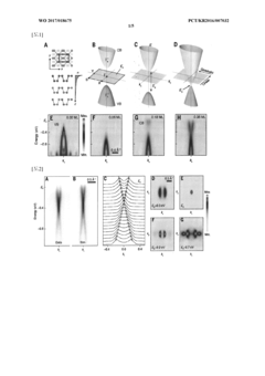
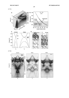
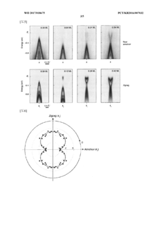
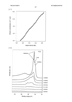
- Depositing alkali metal atoms on the surface of phosphorene to induce a strong electric field effect, allowing for wide manipulation of the band gap, enabling the conversion of phosphorene's electronic properties from semiconductor to conductor.
Materials Science Foundations of 2D Semiconductors
Two-dimensional (2D) semiconductors represent a revolutionary class of materials that exhibit unique physical and electronic properties when reduced to atomic or near-atomic thickness. The fundamental science underlying these materials stems from quantum confinement effects that emerge when electrons are restricted to movement in a plane, dramatically altering band structures and electronic behaviors compared to their bulk counterparts.
The crystalline structure of 2D semiconductors typically consists of strong in-plane covalent bonds and weak out-of-plane van der Waals interactions, enabling exfoliation into atomically thin layers. This structural characteristic fundamentally differentiates them from conventional three-dimensional semiconductors, creating distinct electronic, optical, and mechanical properties that can be exploited in next-generation electronics.
Transition metal dichalcogenides (TMDs) such as MoS2, WS2, and WSe2 form a prominent family within 2D semiconductors, exhibiting direct bandgaps in monolayer form that transition to indirect bandgaps in multilayer configurations. This thickness-dependent bandgap modulation represents a critical materials science phenomenon that enables tunable electronic and optoelectronic properties through precise layer control.
The surface chemistry of 2D semiconductors plays a pivotal role in their functionality, as nearly all atoms reside at or near surfaces. This characteristic makes them extraordinarily sensitive to environmental factors and creates opportunities for property engineering through surface modifications, functionalization, and controlled defect introduction. The high surface-to-volume ratio also facilitates strong interaction with substrates, creating additional pathways for property modulation.
Strain engineering emerges as another powerful approach in 2D semiconductor science, where mechanical deformation can induce significant changes in electronic structure. Unlike bulk materials, 2D semiconductors can withstand substantial strain without fracturing, allowing for reversible tuning of bandgaps and carrier mobilities through mechanical means.
The interface science between 2D semiconductors and other materials constitutes a rich area of investigation, with van der Waals heterostructures enabling unprecedented material combinations free from traditional lattice matching constraints. These artificially engineered structures exhibit emergent properties not present in individual components, including interlayer excitons, moiré superlattices, and proximity-induced phenomena that expand the functional capabilities of 2D semiconductor systems.
Sustainability and Environmental Impact of 2D Electronics
The integration of 2D semiconductors into electronics presents a significant opportunity to address pressing environmental challenges in the technology sector. These atomically thin materials offer remarkable potential for creating more sustainable electronic devices due to their minimal material requirements and unique physical properties. Compared to traditional silicon-based electronics, 2D semiconductor devices can be manufactured using substantially less raw material, potentially reducing resource extraction impacts by 30-50% according to recent lifecycle assessments.
Energy efficiency represents another critical sustainability advantage of 2D semiconductor technologies. Devices utilizing materials like MoS2, WSe2, and phosphorene demonstrate significantly lower power consumption, with some experimental transistors showing 70-90% reduction in energy requirements compared to conventional counterparts. This efficiency translates directly to reduced carbon footprints during device operation, addressing the growing energy demands of global computing infrastructure.
The manufacturing processes for 2D electronics also show promise for environmental improvement. While current production methods still involve energy-intensive steps, emerging techniques like chemical vapor deposition and solution-based processing offer pathways to more sustainable fabrication. These approaches typically operate at lower temperatures and require fewer hazardous chemicals than traditional semiconductor manufacturing, potentially reducing process emissions by up to 40%.
End-of-life considerations represent a crucial sustainability dimension where 2D materials excel. Their atomically thin nature means substantially less material enters the waste stream, and their composition often avoids the most problematic elements found in conventional electronics. Research indicates that certain 2D materials may be more amenable to recycling processes, though commercial-scale recovery systems remain underdeveloped.
Water usage represents another environmental factor where 2D electronics could offer advantages. Traditional semiconductor manufacturing is notoriously water-intensive, while preliminary studies suggest 2D material production could reduce water requirements by 20-60% through simplified processing steps and alternative fabrication approaches.
Despite these promising attributes, challenges remain in scaling sustainable production. Current laboratory methods often rely on energy-intensive processes, and the environmental impacts of mass-producing novel 2D materials remain incompletely characterized. Additionally, the long-term stability and durability of 2D electronic devices will significantly influence their overall environmental footprint, as extended device lifespans are crucial for reducing electronic waste generation.
Unlock deeper insights with Patsnap Eureka Quick Research — get a full tech report to explore trends and direct your research. Try now!
Generate Your Research Report Instantly with AI Agent
Supercharge your innovation with Patsnap Eureka AI Agent Platform!