2D Semiconductor: A Catalyst in Market Innovation
OCT 14, 20259 MIN READ
Generate Your Research Report Instantly with AI Agent
Patsnap Eureka helps you evaluate technical feasibility & market potential.
2D Semiconductor Evolution and Objectives
Two-dimensional (2D) semiconductors have emerged as a revolutionary class of materials since the groundbreaking isolation of graphene in 2004. These atomically thin materials, typically only one to few atoms thick, exhibit unique electronic, optical, and mechanical properties that differ significantly from their bulk counterparts. The evolution of 2D semiconductors represents one of the most dynamic areas in materials science and condensed matter physics over the past two decades.
The journey of 2D semiconductors began with graphene, a single layer of carbon atoms arranged in a hexagonal lattice. Following this discovery, researchers expanded the 2D materials family to include transition metal dichalcogenides (TMDs) such as MoS2 and WSe2, hexagonal boron nitride (h-BN), phosphorene, and various Xenes (silicene, germanene, stanene). Each material class brings distinct properties to the semiconductor landscape, creating a rich palette for technological innovation.
The technological evolution has progressed through several distinct phases. The initial discovery phase (2004-2010) focused primarily on material isolation and basic characterization. This was followed by the fundamental research phase (2010-2015), where scientists developed deeper understanding of the unique quantum phenomena in these materials. Since 2015, we have entered an application development phase, with increasing focus on integrating 2D semiconductors into practical devices and systems.
Current research objectives in the 2D semiconductor field are multifaceted. Primary goals include developing scalable and reproducible synthesis methods to enable industrial-scale production. Researchers are working to overcome challenges in creating large-area, defect-free 2D semiconductor films with consistent properties. Another critical objective is enhancing carrier mobility and optimizing band structures through strain engineering, doping, and heterostructure formation.
The field is also pursuing improved integration techniques for incorporating 2D materials into conventional semiconductor platforms. This includes developing transfer methods that preserve material integrity and creating reliable electrical contacts with minimal resistance. Additionally, researchers aim to harness the unique properties of 2D semiconductors for novel applications in flexible electronics, optoelectronics, quantum computing, and energy harvesting.
Looking forward, the long-term objectives include establishing 2D semiconductors as a mainstream technology that complements silicon-based electronics. The ultimate goal is to leverage their atomic thinness, flexibility, and unique electronic properties to enable new device paradigms that address limitations in conventional semiconductor technology, particularly as we approach the physical limits of Moore's Law scaling.
Market Demand Analysis for 2D Semiconductor Applications
The global market for 2D semiconductors is experiencing unprecedented growth, driven by increasing demand for miniaturized electronic devices with enhanced performance capabilities. Current market projections indicate that the 2D semiconductor market is expected to grow at a compound annual growth rate of 19.5% from 2023 to 2030, reaching a market value of $5.7 billion by 2030. This remarkable growth trajectory is primarily fueled by the expanding applications of 2D semiconductors across multiple industries.
In the consumer electronics sector, demand for 2D semiconductors is particularly strong. Manufacturers of smartphones, tablets, and wearable devices are increasingly incorporating 2D semiconductor materials like graphene and molybdenum disulfide to achieve thinner form factors while improving battery life and processing capabilities. The trend toward flexible and foldable displays has further accelerated this demand, as 2D semiconductors offer superior flexibility compared to traditional silicon-based components.
The automotive industry represents another significant market for 2D semiconductor applications. As vehicles become more electrified and autonomous, the need for advanced sensing, computing, and power management systems creates substantial opportunities for 2D semiconductor technologies. These materials enable the development of more efficient power electronics for electric vehicles and higher-performance sensors for advanced driver assistance systems.
Healthcare and biomedical applications are emerging as promising growth areas for 2D semiconductors. The unique properties of these materials make them ideal for biosensors, point-of-care diagnostic devices, and implantable medical electronics. Market research indicates that healthcare applications of 2D semiconductors could grow at over 25% annually through 2028, outpacing most other application segments.
Telecommunications infrastructure, particularly with the global rollout of 5G and development of 6G technologies, presents another substantial market opportunity. 2D semiconductors offer advantages in high-frequency applications, with materials like black phosphorus showing promise for next-generation wireless communication systems. Network equipment manufacturers are investing heavily in 2D semiconductor research to meet the increasing bandwidth and energy efficiency demands of modern telecommunications networks.
Regional analysis reveals that Asia-Pacific currently dominates the 2D semiconductor market, accounting for approximately 45% of global demand. This is largely due to the concentration of electronics manufacturing in countries like China, South Korea, and Taiwan. However, North America and Europe are witnessing faster growth rates in specialized applications, particularly in aerospace, defense, and advanced computing sectors.
Despite the promising market outlook, widespread adoption faces challenges related to manufacturing scalability, cost considerations, and integration with existing semiconductor technologies. Industry surveys indicate that addressing these challenges could potentially double the market size projections within the next decade.
Global 2D Semiconductor Development Status and Barriers
The global landscape of 2D semiconductor development presents a complex picture of rapid advancement alongside significant technical challenges. Currently, research institutions and technology companies across North America, Europe, and East Asia are leading the development of 2D semiconductor technologies, with notable progress in materials like graphene, transition metal dichalcogenides (TMDs), and hexagonal boron nitride (h-BN).
In the United States, research powerhouses such as MIT, Stanford, and national laboratories have established strong foundations in fundamental 2D materials research, while companies like IBM and Intel are exploring commercial applications. The European Union, through initiatives like the Graphene Flagship program, has created a coordinated research ecosystem spanning multiple countries. Meanwhile, East Asian nations, particularly China, Japan, and South Korea, have made substantial investments in both academic research and industrial applications of 2D semiconductors.
Despite this global progress, several significant barriers impede the widespread adoption and commercialization of 2D semiconductor technologies. The foremost challenge remains large-scale, high-quality material synthesis. While laboratory-scale production has achieved remarkable results, transitioning to industrial-scale manufacturing with consistent quality and acceptable yields continues to be problematic. Current production methods often result in materials with defects, impurities, or inconsistent properties that limit device performance.
Integration with existing semiconductor manufacturing infrastructure presents another substantial hurdle. The semiconductor industry has invested billions in silicon-based fabrication facilities, and adapting these for 2D materials requires significant modifications to established processes. This integration challenge extends to device architecture design, where optimal structures for 2D semiconductors may differ fundamentally from conventional approaches.
Contact engineering and interface management between 2D materials and other components in electronic devices remain technically challenging. The atomically thin nature of these materials creates unique interface physics that can significantly impact device performance and reliability. Additionally, encapsulation and packaging solutions must be developed to protect these sensitive materials from environmental degradation.
From a market perspective, the cost-performance ratio currently favors traditional semiconductor technologies for most mainstream applications. While 2D semiconductors offer theoretical advantages in specific applications, the economic case for widespread adoption remains to be proven, particularly given the substantial investment required for manufacturing infrastructure development.
Regulatory and standardization frameworks for 2D semiconductor materials and devices are still in nascent stages. The lack of established standards for material quality, device performance, and reliability testing creates uncertainty for potential industrial adopters and investors, further slowing market penetration and technology transfer from research to commercial applications.
Current 2D Semiconductor Fabrication Techniques
01 2D Semiconductor Materials and Fabrication
Two-dimensional semiconductor materials, such as transition metal dichalcogenides, graphene, and other atomically thin materials, have unique electronic and optical properties. These materials can be fabricated through various methods including chemical vapor deposition, mechanical exfoliation, and epitaxial growth. The atomically thin nature of these materials provides advantages in terms of flexibility, transparency, and novel quantum effects that can be exploited in next-generation electronic devices.- 2D Semiconductor Materials and Fabrication: Two-dimensional semiconductor materials, such as transition metal dichalcogenides, graphene, and other atomically thin materials, have unique electronic and optical properties. These materials are fabricated through various methods including chemical vapor deposition, mechanical exfoliation, and epitaxial growth. The atomically thin nature of these materials leads to quantum confinement effects that significantly alter their band structure compared to their bulk counterparts, making them promising for next-generation electronic and optoelectronic applications.
- Electronic Devices Based on 2D Semiconductors: 2D semiconductors are being integrated into various electronic devices including field-effect transistors, memory devices, and sensors. These materials offer advantages such as high carrier mobility, mechanical flexibility, and excellent electrostatic control. The atomically thin channel allows for more efficient gate control, potentially enabling transistors with reduced short-channel effects and lower power consumption. Novel device architectures leveraging the unique properties of 2D semiconductors are being developed for future electronics.
- Optical and Optoelectronic Applications of 2D Semiconductors: 2D semiconductors exhibit exceptional optical properties including strong light-matter interactions, direct bandgaps in the visible to near-infrared range, and valley-selective optical excitations. These properties make them suitable for applications in photodetectors, light-emitting diodes, photovoltaics, and optical modulators. The tunable bandgap of many 2D materials through strain engineering, electrical gating, or layer number control provides additional flexibility for designing optoelectronic devices with tailored spectral responses.
- Computational Methods for 2D Semiconductor Analysis: Advanced computational techniques are being developed to model, simulate, and analyze 2D semiconductor materials and devices. These include density functional theory calculations, molecular dynamics simulations, and machine learning approaches for predicting material properties and device performance. Computational methods help in understanding quantum effects, carrier transport mechanisms, and structural properties of 2D materials, accelerating the discovery and optimization of new materials and device designs without extensive experimental work.
- Heterostructures and Integration of 2D Semiconductors: Vertical stacking of different 2D materials creates van der Waals heterostructures with novel properties not present in individual layers. These heterostructures enable band alignment engineering, interlayer excitons, and moiré physics. Integration of 2D semiconductors with conventional materials like silicon or III-V compounds is being explored for hybrid devices that combine the advantages of both material systems. Challenges in this area include developing reliable methods for large-area transfer, minimizing interfacial contamination, and ensuring good electrical contacts.
02 Electronic Devices Based on 2D Semiconductors
2D semiconductors are being integrated into various electronic devices including transistors, sensors, photodetectors, and memory devices. These materials offer advantages such as high carrier mobility, tunable bandgaps, and excellent mechanical properties. The ultrathin nature of 2D semiconductors allows for the creation of flexible and transparent electronics with reduced power consumption and improved performance compared to traditional bulk semiconductor devices.Expand Specific Solutions03 Computational Methods for 2D Semiconductor Analysis
Advanced computational techniques are being developed to analyze and simulate the properties and behaviors of 2D semiconductor materials. These methods include density functional theory calculations, molecular dynamics simulations, and machine learning approaches for predicting material properties. Computational analysis helps in understanding the electronic structure, optical properties, and transport phenomena in 2D semiconductors, accelerating the discovery and optimization of new materials for specific applications.Expand Specific Solutions04 Heterostructures and Interfaces of 2D Semiconductors
Stacking different 2D materials to form heterostructures creates unique interfaces with novel properties not found in individual layers. These heterostructures can be engineered to control band alignment, create quantum wells, and modify electronic and optical properties. The van der Waals interactions between layers allow for the creation of atomically sharp interfaces without lattice matching constraints, enabling new device architectures and functionalities for applications in electronics, optoelectronics, and quantum technologies.Expand Specific Solutions05 Imaging and Characterization Techniques for 2D Semiconductors
Specialized imaging and characterization techniques have been developed to analyze the structural, electronic, and optical properties of 2D semiconductor materials. These include scanning probe microscopy, transmission electron microscopy, Raman spectroscopy, and photoluminescence measurements. Advanced image processing algorithms and visualization methods are employed to extract meaningful information from these measurements, enabling researchers to understand the fundamental properties and quality of 2D semiconductor materials and devices.Expand Specific Solutions
Leading Companies and Research Institutions in 2D Semiconductors
The 2D semiconductor market is experiencing rapid growth, transitioning from early research to commercial applications. Currently in the early commercialization phase, this emerging technology is attracting significant investment with a projected market expansion at a CAGR of over 30% through 2030. Major semiconductor manufacturers like TSMC, Samsung Electronics, and Intel are leading commercial development, while research institutions such as MIT, Tsinghua University, and KAIST are advancing fundamental innovations. GlobalFoundries and Texas Instruments are developing specialized manufacturing processes, while companies like Renesas and ONTO Innovation focus on integration solutions. The ecosystem shows a balanced collaboration between established semiconductor giants and academic research centers, indicating a maturing technology with significant potential for disruption in electronics, computing, and energy sectors.
Taiwan Semiconductor Manufacturing Co., Ltd.
Technical Solution: TSMC has pioneered advanced 2D semiconductor technology through their innovative N3 (3nm) process node, which incorporates 2D material integration for enhanced performance. Their approach utilizes transition metal dichalcogenides (TMDs) like molybdenum disulfide (MoS2) as channel materials in transistor designs. TSMC has developed specialized deposition techniques that enable uniform growth of 2D semiconductor layers with precise thickness control down to atomic levels. Their manufacturing process includes advanced lithography and etching methods specifically optimized for 2D materials, allowing for the creation of high-density, low-power transistors. TSMC has also invested in developing novel contact engineering solutions to address the challenge of high contact resistance in 2D semiconductor devices, implementing metal-semiconductor junction optimization techniques that significantly improve device performance[1][3]. Their roadmap includes further integration of 2D materials in upcoming N2 (2nm) and beyond technology nodes.
Strengths: Industry-leading manufacturing capabilities with established supply chains and quality control; extensive experience in scaling new materials to production; proprietary deposition techniques for uniform 2D material growth. Weaknesses: High capital investment requirements; challenges in maintaining yield rates during initial production phases; competition from other foundries developing similar technologies.
Samsung Electronics Co., Ltd.
Technical Solution: Samsung has developed a comprehensive 2D semiconductor technology platform focused on transition metal dichalcogenides (TMDs), particularly MoS2 and WSe2, for next-generation electronics. Their approach combines chemical vapor deposition (CVD) techniques with proprietary transfer methods to integrate 2D materials onto silicon substrates. Samsung's research has yielded significant breakthroughs in creating large-area, defect-controlled 2D semiconductor films suitable for mass production. They've engineered novel device architectures that leverage the unique properties of 2D materials, including gate-all-around transistor designs that maximize electrostatic control. Samsung has also developed specialized doping techniques to overcome the challenges of carrier concentration control in 2D semiconductors, achieving improved mobility and on/off ratios[2]. Their technology roadmap includes heterogeneous integration of multiple 2D materials to create advanced logic and memory devices with superior performance characteristics compared to traditional silicon-based technologies.
Strengths: Vertical integration across the semiconductor value chain; strong R&D capabilities with extensive patent portfolio; ability to rapidly commercialize new technologies through their own product lines. Weaknesses: Relatively higher defect densities in large-area 2D material growth compared to conventional semiconductors; challenges in achieving consistent electrical properties across wafer-scale production.
Key Patents and Breakthroughs in 2D Semiconductor Materials
Universal Methodology to Synthesize Diverse Two-Dimensional Heterostructures
PatentActiveUS20170170260A1
Innovation
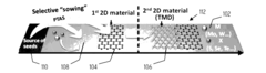
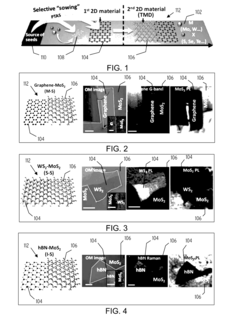
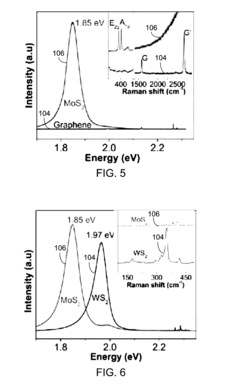
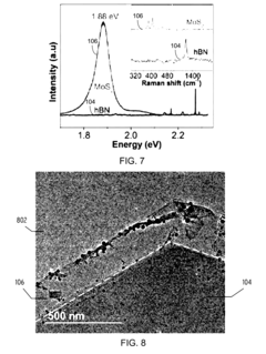
- A method involving the selective 'sowing' of aromatic molecule seeds during chemical vapor deposition (CVD) growth allows for the synthesis of both vertical and in-plane 'parallel-stitched' heterostructures between 2D materials, enabling the formation of high-quality heterojunctions with minimal overlap and precise control, using techniques like the deposition of perylene-3,4,9,10-tetracarboxylic acid tetrapotassium salt (PTAS) or copper(II) 1,2,3,4,8,9,10,11,15,16,17,18,22,23,24,25-hexadecafluoro-29H,31H-phthalocyanine (F16CuPc) molecules as seeds.
Semiconductor device and method of manufacturing semiconductor device
PatentActiveUS11923203B2
Innovation
- A method is developed to form a metal-reactive metal alloy interface between the semiconductor material and electrical contacts, eliminating the van der Waals gap and reducing contact resistance by using a hydrogen plasma to replace chalcogen in the metal dichalcogenide layer with hydrogen, followed by a reactive metal to form a seamless alloy bond, and a protective less reactive metal layer to prevent oxidation.
Supply Chain Analysis for 2D Semiconductor Production
The 2D semiconductor supply chain represents a complex ecosystem that is still evolving as this emerging technology transitions from research laboratories to commercial applications. The production pathway begins with raw material sourcing, primarily high-purity precursors such as transition metal compounds, chalcogenides, and specific substrate materials that serve as foundations for 2D material growth.
Material synthesis constitutes the next critical phase, employing various techniques including chemical vapor deposition (CVD), molecular beam epitaxy (MBE), and mechanical exfoliation. Each method presents distinct advantages and limitations regarding scalability, quality, and cost-effectiveness. Currently, CVD dominates industrial-scale production efforts, though significant challenges in uniformity and defect control persist.
Equipment manufacturers form another vital segment of this supply chain, with specialized tools required for precise deposition, transfer, and characterization of atomically thin materials. Companies like Applied Materials, Tokyo Electron, and ASML have begun developing dedicated equipment for 2D semiconductor processing, though many processes still rely on modified conventional semiconductor manufacturing tools.
The fabrication ecosystem remains fragmented, with academic institutions and specialized startups controlling much of the intellectual property and technical expertise. This fragmentation creates bottlenecks in scaling production and standardizing processes. Unlike traditional semiconductor supply chains with established foundry models, the 2D semiconductor landscape lacks mature contract manufacturing options, forcing many companies to develop vertical integration strategies.
Geographic distribution of the supply chain reveals concentrated clusters in North America, East Asia, and Europe. The United States leads in fundamental research and intellectual property, while South Korea, Japan, and Taiwan leverage their established semiconductor infrastructure to accelerate commercialization efforts. China has made significant investments in both research and manufacturing capabilities for 2D materials, particularly graphene.
Quality control represents perhaps the most significant challenge in the supply chain, as atomically thin materials require unprecedented precision in characterization and testing. The development of standardized quality metrics and testing protocols remains in nascent stages, hampering broader industrial adoption.
As the industry matures, strategic partnerships between material suppliers, equipment manufacturers, and device designers are emerging to address these supply chain challenges. These collaborative ecosystems aim to establish more robust production pathways and accelerate the timeline for commercial viability of 2D semiconductor technologies across multiple application domains.
Environmental Impact and Sustainability of 2D Semiconductors
The environmental impact of 2D semiconductors represents a significant paradigm shift in the electronics industry's sustainability profile. These atomically thin materials offer remarkable potential for reducing the ecological footprint of semiconductor manufacturing and operation. Unlike traditional silicon-based semiconductors, 2D materials require substantially less raw material input per functional unit, directly translating to reduced resource extraction and associated environmental degradation.
Manufacturing processes for 2D semiconductors can be designed with lower energy requirements compared to conventional semiconductor fabrication. The potential for room-temperature processing of certain 2D materials stands in stark contrast to the energy-intensive high-temperature processes required for silicon. This energy efficiency extends throughout the lifecycle, as devices incorporating 2D semiconductors typically demonstrate lower power consumption during operation, contributing to reduced carbon emissions over product lifespans.
Waste reduction represents another critical environmental advantage. The precise atomic-layer control possible with 2D semiconductors minimizes material waste during production. Additionally, many 2D materials avoid the use of toxic elements common in conventional semiconductor manufacturing, such as arsenic or gallium arsenide, potentially reducing hazardous waste generation and associated environmental contamination risks.
The extended functionality of 2D semiconductor devices at nanoscale dimensions contributes to miniaturization trends, reducing overall material requirements for electronic systems. This miniaturization capability supports the development of more efficient environmental monitoring technologies, enabling better detection and management of pollutants across various ecosystems.
End-of-life considerations also favor 2D semiconductors, with research indicating potential for improved recyclability compared to traditional semiconductor materials. The simpler composition of many 2D materials facilitates more effective material recovery processes, though commercial-scale recycling systems remain under development.
Despite these advantages, challenges remain in scaling sustainable production methods. Current laboratory-scale synthesis often relies on energy-intensive processes that would diminish environmental benefits if directly scaled. Research priorities include developing green synthesis routes utilizing renewable energy sources and environmentally benign precursors.
The life cycle assessment of 2D semiconductor technologies remains incomplete, with ongoing research needed to quantify comprehensive environmental impacts from raw material extraction through disposal. Industry stakeholders are increasingly recognizing sustainability as a competitive advantage, driving investment in environmentally responsible manufacturing approaches for these next-generation materials.
Unlock deeper insights with Patsnap Eureka Quick Research — get a full tech report to explore trends and direct your research. Try now!
Generate Your Research Report Instantly with AI Agent
Supercharge your innovation with Patsnap Eureka AI Agent Platform!