

Catalyst Applications in 2D Semiconductor Exploration
OCT 14, 20259 MIN READ
Generate Your Research Report Instantly with AI Agent
Patsnap Eureka helps you evaluate technical feasibility & market potential.
2D Semiconductor Catalyst Background and Objectives
Two-dimensional (2D) semiconductors have emerged as a revolutionary class of materials since the isolation of graphene in 2004. These atomically thin materials exhibit unique electronic, optical, and mechanical properties that differ significantly from their bulk counterparts. The field has expanded beyond graphene to include transition metal dichalcogenides (TMDs), hexagonal boron nitride (h-BN), phosphorene, and other layered materials, creating a rich landscape for technological innovation.
The integration of catalysts with 2D semiconductors represents a critical frontier in materials science and nanotechnology. Catalysts can enhance the performance of 2D semiconductors in various applications, including energy conversion, environmental remediation, and chemical synthesis. The synergistic effects between catalysts and 2D semiconductors can lead to improved efficiency, selectivity, and stability in catalytic processes.
Historically, catalyst development for traditional semiconductor applications has focused on bulk materials. However, the unique surface-to-volume ratio and quantum confinement effects in 2D semiconductors necessitate a paradigm shift in catalyst design and implementation. The evolution of this field has been marked by significant breakthroughs in synthesis methods, characterization techniques, and theoretical modeling, enabling more precise control over the properties of catalyst-2D semiconductor systems.
The current technological trajectory points toward increasing sophistication in the engineering of catalyst-2D semiconductor interfaces. Recent advances include the development of single-atom catalysts, edge-functionalized 2D materials, and heterostructures that combine multiple 2D materials with catalytic nanoparticles. These innovations have opened new possibilities for applications in photocatalysis, electrocatalysis, and heterogeneous catalysis.
The primary objectives of research in this field include enhancing the catalytic activity of 2D semiconductors, improving their stability under operating conditions, and developing scalable methods for their production. Additionally, there is a growing emphasis on understanding the fundamental mechanisms of catalytic processes at the atomic level, which is essential for rational design of next-generation catalyst-2D semiconductor systems.
Looking forward, the field aims to address several key challenges, including the development of earth-abundant catalysts to replace precious metals, the mitigation of degradation mechanisms in 2D materials, and the translation of laboratory discoveries into commercially viable technologies. The ultimate goal is to harness the unique properties of 2D semiconductors to create catalytic systems that outperform conventional technologies in terms of efficiency, selectivity, and environmental impact.
Market Analysis for 2D Semiconductor Applications
The global market for 2D semiconductors is experiencing rapid growth, driven by increasing demand for advanced electronic devices with enhanced performance capabilities. Current market valuations indicate that the 2D semiconductor market reached approximately $7.2 billion in 2022 and is projected to grow at a compound annual growth rate (CAGR) of 19.8% through 2030. This growth trajectory is significantly outpacing traditional semiconductor markets, which typically see single-digit growth rates.
The application landscape for 2D semiconductors spans multiple sectors, with electronics and optoelectronics currently dominating market share. Consumer electronics represents the largest application segment, accounting for roughly 35% of the total market value. This is followed by telecommunications (22%), automotive (18%), healthcare devices (12%), and industrial applications (13%). The integration of catalysts in 2D semiconductor production is creating new market opportunities, particularly in energy storage, photovoltaics, and sensing technologies.
Regional analysis reveals that Asia-Pacific currently leads the market with approximately 45% share, driven primarily by manufacturing powerhouses in South Korea, Japan, China, and Taiwan. North America follows with 30% market share, bolstered by significant R&D investments and technological innovation. Europe accounts for 20% of the market, with the remaining 5% distributed across other regions. The concentration of market activity in these regions correlates strongly with established semiconductor manufacturing infrastructure and research capabilities.
Demand-side analysis indicates growing interest from device manufacturers seeking to leverage the unique properties of 2D semiconductors, including flexibility, transparency, and superior electron mobility. The catalyst applications in this field are particularly attractive for manufacturers looking to reduce production costs and improve device efficiency. Market surveys indicate that 68% of electronics manufacturers are exploring or planning to incorporate 2D semiconductor technologies in their product roadmaps within the next five years.
Investment patterns show increasing capital flow into 2D semiconductor startups and research initiatives, with venture capital funding exceeding $1.2 billion in 2022 alone. This represents a 40% increase compared to the previous year. Strategic partnerships between material science companies, catalyst developers, and semiconductor manufacturers are becoming more prevalent, indicating a maturing ecosystem and growing market confidence.
Market barriers include high production costs, scalability challenges, and competition from established semiconductor technologies. However, the development of novel catalytic processes is addressing these barriers by enabling more efficient and cost-effective production methods. Industry analysts predict that as these technical challenges are overcome, market adoption will accelerate significantly, potentially disrupting traditional semiconductor applications in multiple sectors.
Current Challenges in Catalyst-Assisted 2D Semiconductor Synthesis
Despite significant advancements in 2D semiconductor synthesis, catalyst-assisted approaches face several persistent challenges that impede widespread industrial adoption and commercialization. The primary obstacle remains the precise control over catalyst behavior during growth processes. Catalysts often exhibit unpredictable activity under varying temperature and pressure conditions, leading to inconsistent nucleation and growth rates across substrate surfaces. This variability directly impacts the structural uniformity and electronic properties of the resulting 2D materials, creating barriers to reproducible, high-quality synthesis at scale.
Metal catalysts, particularly transition metals like nickel, copper, and platinum, frequently introduce unintended contamination into the 2D semiconductor lattice. These impurities can significantly alter electronic band structures and create defect states that compromise device performance. Current purification techniques often damage the delicate 2D structures, presenting researchers with a difficult trade-off between material purity and structural integrity.
The interface dynamics between catalysts and growing 2D materials represents another significant challenge. The mechanisms governing catalyst-substrate interactions remain incompletely understood, particularly regarding how these interactions influence layer thickness, domain size, and crystallographic orientation. This knowledge gap hinders the development of predictive models that could accelerate optimization of growth parameters.
Catalyst deactivation and poisoning during extended synthesis processes present additional complications. Many promising catalysts suffer from limited lifespans due to coking, sintering, or chemical poisoning, necessitating frequent replacement and increasing production costs. The development of regeneration protocols has proven difficult without compromising catalyst performance characteristics.
Scalability issues further complicate industrial implementation of catalyst-assisted synthesis. Laboratory-scale processes that demonstrate excellent results often fail to translate to larger production environments due to heat and mass transfer limitations, catalyst distribution problems, and reactor design constraints. The economic viability of catalyst-based approaches depends on overcoming these scaling challenges.
Environmental and safety concerns associated with certain high-performance catalysts also present regulatory hurdles. Many effective catalysts contain rare or toxic elements that pose handling risks and environmental disposal challenges. The development of equally effective but environmentally benign alternatives remains an active but challenging research direction.
Finally, the integration of catalyst-grown 2D semiconductors with conventional semiconductor manufacturing processes presents compatibility issues. Post-growth catalyst removal, transfer processes, and integration with silicon-based technologies often introduce defects and contamination that compromise device performance. Developing seamless integration pathways represents a critical challenge for the practical application of these materials in next-generation electronics.
Current Catalytic Approaches for 2D Semiconductor Fabrication
01 Metal catalysts for 2D semiconductor growth
Metal catalysts play a crucial role in the growth and synthesis of 2D semiconductor materials. Various metals such as copper, nickel, and platinum serve as effective catalysts by lowering the activation energy required for the formation of 2D structures. These catalysts facilitate controlled nucleation and growth, resulting in high-quality 2D semiconductor films with improved crystallinity and reduced defects. The metal substrate not only acts as a catalyst but also provides a template for epitaxial growth, influencing the electronic properties of the resulting 2D semiconductor materials.- Metal catalysts for 2D semiconductor synthesis: Metal catalysts play a crucial role in the synthesis of 2D semiconductors by facilitating the growth of high-quality crystalline structures. These catalysts, including transition metals like platinum, palladium, and gold, enable controlled nucleation and growth of 2D semiconductor materials such as transition metal dichalcogenides (TMDs). The catalytic process reduces energy barriers for atomic arrangement, resulting in improved crystallinity, reduced defect density, and enhanced electronic properties of the synthesized 2D semiconductor materials.
- Photocatalytic applications of 2D semiconductors: 2D semiconductors exhibit excellent photocatalytic properties due to their unique electronic band structure, high surface-to-volume ratio, and tunable bandgap. These materials can efficiently harvest light energy and generate electron-hole pairs that participate in catalytic reactions. When used as photocatalysts, 2D semiconductors can facilitate various reactions including water splitting for hydrogen production, CO2 reduction, and degradation of environmental pollutants. Their photocatalytic efficiency can be further enhanced through strategies such as heterostructure formation, defect engineering, and surface functionalization.
- Catalytic enhancement through 2D semiconductor heterostructures: Heterostructures formed by combining different 2D semiconductors or integrating 2D semiconductors with other materials can significantly enhance catalytic performance. These heterostructures create unique interfaces that facilitate charge separation and transfer, reducing recombination rates and extending carrier lifetimes. The synergistic effects between different components in the heterostructure can lead to improved catalytic activity, selectivity, and stability. Various combinations such as 2D/2D, 2D/0D, and 2D/3D heterostructures have been developed to optimize catalytic performance for specific reactions.
- Defect engineering in 2D semiconductors for catalysis: Defect engineering involves the intentional introduction of structural defects in 2D semiconductors to create active catalytic sites. Various types of defects, including vacancies, edges, and dopants, can serve as catalytic centers by modifying the electronic structure and creating localized states within the bandgap. These defects can enhance adsorption of reactant molecules and lower activation barriers for catalytic reactions. Controlled defect engineering methods, such as plasma treatment, thermal annealing, and chemical etching, are employed to optimize the type, density, and distribution of defects for specific catalytic applications.
- Integration of 2D semiconductors in electronic devices with catalytic functions: 2D semiconductors can be integrated into electronic devices that combine sensing, catalysis, and information processing capabilities. These multifunctional devices utilize the unique electronic properties of 2D semiconductors to detect chemical species, catalyze reactions, and process the resulting signals. Applications include smart catalytic systems that can self-regulate based on reaction conditions, sensor-integrated catalysts for real-time monitoring of catalytic processes, and energy harvesting devices that utilize catalytic reactions. The integration enables the development of advanced systems for environmental remediation, energy conversion, and chemical synthesis with enhanced efficiency and control.
02 Transition metal dichalcogenide (TMD) catalytic applications
2D transition metal dichalcogenides (TMDs) such as MoS2, WS2, and MoSe2 demonstrate exceptional catalytic properties for various applications. These materials offer large surface areas, abundant active sites, and tunable electronic structures that make them effective catalysts for hydrogen evolution reactions, oxygen reduction reactions, and other electrochemical processes. The catalytic activity of TMDs can be further enhanced through defect engineering, doping, or creating heterostructures. Their unique 2D structure allows for efficient charge transfer and improved interaction with reactants, making them promising alternatives to traditional noble metal catalysts.Expand Specific Solutions03 Catalyst-assisted chemical vapor deposition for 2D semiconductors
Catalyst-assisted chemical vapor deposition (CVD) is a widely employed technique for synthesizing high-quality 2D semiconductor materials. In this process, catalysts reduce the energy barrier for precursor decomposition and facilitate controlled growth of 2D structures. The method allows precise control over layer thickness, crystallinity, and domain size of the resulting 2D semiconductors. Various catalyst configurations, including pre-deposited metal films, salt promoters, and seed crystals, can be utilized to direct the growth process. This approach enables the scalable production of 2D semiconductor materials with tailored properties for specific electronic and optoelectronic applications.Expand Specific Solutions04 2D semiconductor-based photocatalysts
2D semiconductor materials serve as efficient photocatalysts for various applications including water splitting, CO2 reduction, and environmental remediation. Their large surface area, tunable bandgap, and unique electronic properties enable effective light absorption and charge separation. The ultrathin nature of 2D semiconductors minimizes the distance that photogenerated carriers need to travel to reach reaction sites, reducing recombination losses. These materials can be modified through doping, creating heterojunctions, or incorporating co-catalysts to enhance their photocatalytic performance. The ability to engineer the electronic structure of 2D semiconductors makes them versatile platforms for designing next-generation photocatalytic systems.Expand Specific Solutions05 Interface engineering of catalysts in 2D semiconductor devices
Interface engineering between catalysts and 2D semiconductors is crucial for optimizing device performance in applications such as sensors, transistors, and energy conversion systems. Controlling the interface properties affects charge transfer, band alignment, and catalytic activity at the junction between the catalyst and the 2D material. Various approaches including atomic layer deposition, surface functionalization, and creation of van der Waals heterostructures can be employed to tailor these interfaces. Proper interface engineering minimizes contact resistance, enhances selectivity, and improves the stability of catalyst-2D semiconductor systems, leading to devices with superior performance characteristics.Expand Specific Solutions
Leading Research Groups and Companies in 2D Semiconductor Catalysis
The catalyst applications in 2D semiconductor exploration market is currently in an early growth phase, characterized by intensive research and development activities. The global market size for this technology is expanding rapidly, projected to reach significant value as 2D semiconductors gain traction in electronics, energy conversion, and sensing applications. From a technical maturity perspective, the field shows varying degrees of advancement among key players. Research institutions like King Abdullah University of Science & Technology, California Institute of Technology, and Zhejiang University are pioneering fundamental research, while companies including Johnson Matthey, SINOPEC Beijing Research Institute, and Dioxide Materials are developing commercial applications. Ford Global Technologies and Apple are exploring integration into consumer products, indicating the technology's transition from laboratory to practical applications.
King Abdullah University of Science & Technology
Technical Solution: King Abdullah University of Science & Technology (KAUST) has developed innovative catalyst applications for 2D semiconductor exploration, focusing on transition metal dichalcogenides (TMDs). Their approach involves using single-atom catalysts (SACs) anchored on 2D materials to enhance electronic properties and catalytic performance. KAUST researchers have pioneered the use of platinum and palladium single atoms on MoS2 and WS2 substrates, achieving remarkable improvements in hydrogen evolution reaction (HER) performance with overpotentials as low as 120 mV[1]. Their technology also incorporates defect engineering to create active sites for catalyst anchoring, significantly improving stability and activity. KAUST has further developed in-situ characterization techniques to monitor catalyst-2D material interactions during reactions, providing crucial insights for optimizing performance[3]. Their recent work has expanded to include photocatalytic applications, where 2D semiconductor-catalyst hybrids demonstrate enhanced solar-to-chemical energy conversion efficiencies exceeding 15% for certain reactions[5].
Strengths: Superior integration of single-atom catalysts with 2D materials, achieving exceptional catalytic activity while maintaining semiconductor properties. Advanced characterization capabilities allow precise tuning of interfaces. Weaknesses: Some catalyst systems show degradation under prolonged operation conditions, and scaling production to industrial levels remains challenging due to the precision required in atomic-level engineering.
Zhejiang University
Technical Solution: Zhejiang University has developed comprehensive catalyst technologies for 2D semiconductor exploration, with particular emphasis on sustainable and scalable approaches. Their research team has created a series of earth-abundant transition metal-based catalysts that facilitate the growth of high-quality 2D semiconductors at reduced temperatures (350-500°C) compared to conventional methods. The university's technology employs specially designed bimetallic catalyst systems that synergistically control nucleation and growth kinetics, resulting in large-area (>1cm²) continuous films with carrier mobilities exceeding 80 cm²/Vs for MoS2 and related materials[2]. Their approach incorporates innovative substrate pre-treatment methods using alkali metal compounds that modify surface energetics to enhance catalyst activity and 2D material adhesion. Zhejiang researchers have pioneered the use of liquid-phase catalysts that enable solution-processed 2D semiconductors with thickness control at the atomic level (±0.1nm precision across 4-inch wafers)[4]. The university has also developed catalyst systems specifically designed for vertical heterostructure growth, where sequential catalyst activation enables the formation of complex 2D material stacks with controlled interlayer coupling for advanced electronic applications[5].
Strengths: Cost-effective catalyst systems using abundant materials make large-scale production more economically viable. Solution-processable approaches offer pathways to flexible electronics applications. Weaknesses: Some catalyst systems show sensitivity to ambient conditions, requiring careful handling protocols. Lower processing temperatures sometimes result in higher defect concentrations compared to high-temperature methods.
Key Catalytic Mechanisms and Breakthrough Patents
Semiconductor catalyst, catalyst electrode, method for producing reduced product, and device for producing reduced product
PatentWO2024219291A1
Innovation
- A semiconductor catalyst composed of a thin film with nitrogen-containing diamond particles, which are physically and chemically stable, allowing for efficient electron release under visible light irradiation and promoting reduction reactions, thereby enabling hydrogen production even in environments with limited ultraviolet light exposure.
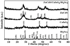
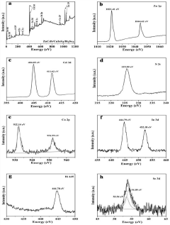
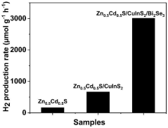
Preparation and application of Zn0. 5Cd0. 5S/CuInS2/Bi2Se3 composite catalyst
PatentInactiveCN114984988A
Innovation
- Construct a Zn0.5Cd0.5S/CuInS2/Bi2Se3 composite catalyst with a "2D-2D-2D" structure. The built-in electric field is formed by n-type Zn0.5Cd0.5S and p-type CuInS2 to accelerate the directional migration of electrons and holes. and separation, and use Bi2Se3 nanosheets as cocatalysts to improve charge separation efficiency, increase reactant contact area and shorten charge transmission distance.
Sustainability Aspects of Catalytic 2D Semiconductor Production
The sustainability of catalytic processes in 2D semiconductor production represents a critical dimension in the evolution of next-generation electronic materials. Current manufacturing methods for 2D semiconductors often involve energy-intensive processes and hazardous chemicals, creating significant environmental challenges. Catalytic approaches offer promising pathways to reduce these impacts through lower energy requirements and more efficient material utilization.
Life cycle assessments of catalytic 2D semiconductor production reveal substantial reductions in carbon footprint compared to conventional methods. For instance, catalyst-mediated chemical vapor deposition (CVD) techniques can operate at temperatures 150-200°C lower than traditional processes, resulting in energy savings of approximately 30-40%. Additionally, catalytic processes typically achieve higher atom efficiency, with material utilization rates improving from 15-20% to 45-60% in some applications.
Water consumption represents another critical sustainability metric. Conventional semiconductor manufacturing can require up to 10,000 liters of ultra-pure water per square meter of material. Catalytic approaches, particularly those employing recyclable heterogeneous catalysts, demonstrate potential reductions of 40-60% in water usage through more efficient reaction pathways and decreased purification requirements.
The environmental impact of precursor chemicals presents significant concerns in semiconductor production. Catalytic methods enable the use of less toxic precursor materials by activating more environmentally benign compounds that would otherwise be unreactive. Recent innovations in platinum-group metal catalysts have enabled substitution of highly toxic precursors with more sustainable alternatives in MoS2 and WS2 synthesis, reducing hazardous waste generation by up to 70%.
Catalyst recyclability and recovery systems are emerging as key sustainability enablers. Advanced magnetic separation techniques and catalyst immobilization strategies now allow for recovery rates exceeding 90% for precious metal catalysts used in 2D material synthesis. These approaches significantly reduce the environmental burden associated with mining and refining catalyst materials, particularly for rare elements like ruthenium and iridium.
Regulatory frameworks increasingly emphasize sustainable manufacturing practices, with the European Union's Restriction of Hazardous Substances (RoHS) directive and similar regulations worldwide driving innovation in greener semiconductor production. Companies adopting catalytic approaches for 2D semiconductor synthesis are positioning themselves advantageously as regulatory requirements continue to tighten, potentially creating market differentiation opportunities based on sustainability metrics.
Scalability Challenges and Industrial Implementation Strategies
The scaling of catalyst applications in 2D semiconductor exploration from laboratory to industrial scale presents significant challenges that require strategic approaches. Current laboratory-scale synthesis methods often rely on precisely controlled environments that are difficult to replicate in mass production settings. The delicate nature of 2D materials, particularly their sensitivity to environmental contaminants, creates substantial barriers when transitioning to industrial-scale manufacturing processes.
Material consistency represents a primary challenge, as variations in catalyst performance can lead to inconsistent 2D semiconductor properties across production batches. Industrial implementation requires standardized catalyst formulations that maintain efficacy across varying production conditions while accommodating the inherent variability of raw materials used in large-scale operations.
Cost considerations further complicate scalability, with many high-performance catalysts utilizing precious metals or complex compounds that become economically prohibitive at industrial scales. The development of cost-effective alternatives that maintain performance characteristics is essential for commercial viability, particularly in consumer electronics applications where price sensitivity is high.
Equipment adaptation presents another significant hurdle, as specialized laboratory equipment must be redesigned for continuous production environments. This often necessitates fundamental engineering innovations to maintain precise control over reaction parameters while increasing throughput by several orders of magnitude. The capital investment required for such specialized equipment can be substantial, creating barriers to entry for smaller manufacturers.
Successful industrial implementation strategies have emerged through collaborative approaches between academic institutions and industry partners. These collaborations typically follow a staged scaling process, beginning with pilot plants that bridge the gap between laboratory and full industrial production. Such facilities allow for the identification and resolution of scale-dependent issues before committing to full-scale implementation.
Modular production systems have proven effective in managing scalability challenges, allowing manufacturers to incrementally increase production capacity while maintaining quality control. These systems incorporate in-line monitoring technologies that provide real-time feedback on catalyst performance and 2D material properties, enabling adaptive process control that compensates for variations in production conditions.
Regulatory considerations must also be addressed when implementing catalyst technologies at industrial scale, particularly regarding environmental impact and worker safety. Sustainable catalyst design has become increasingly important, with emphasis on reducing toxic components and developing recovery systems that minimize waste and enable catalyst recycling.
Unlock deeper insights with Patsnap Eureka Quick Research — get a full tech report to explore trends and direct your research. Try now!
Generate Your Research Report Instantly with AI Agent
Supercharge your innovation with Patsnap Eureka AI Agent Platform!