

2D Semiconductor Contributions to Pharmaceutical Tech
OCT 14, 202510 MIN READ
Generate Your Research Report Instantly with AI Agent
Patsnap Eureka helps you evaluate technical feasibility & market potential.
2D Semiconductor Evolution and Pharmaceutical Applications
Two-dimensional (2D) semiconductors have undergone remarkable evolution since the groundbreaking isolation of graphene in 2004. This atomically thin carbon layer sparked a revolution in materials science, leading to the discovery and synthesis of numerous other 2D materials including transition metal dichalcogenides (TMDs), hexagonal boron nitride (h-BN), and phosphorene. The unique properties of these materials—including exceptional electron mobility, mechanical flexibility, and tunable bandgaps—have positioned them as transformative elements across multiple industries.
In pharmaceutical applications, the evolution of 2D semiconductors has created unprecedented opportunities for drug delivery, biosensing, and therapeutic interventions. Initially, graphene oxide was the primary 2D material explored for pharmaceutical purposes due to its large surface area and functional groups that facilitate drug loading. As the field matured, more sophisticated 2D materials emerged with enhanced biocompatibility and targeted delivery capabilities.
The integration of 2D semiconductors into pharmaceutical technology has evolved through several distinct phases. The first phase (2004-2010) focused primarily on fundamental research and characterization of these materials. The second phase (2010-2015) saw initial explorations of biomedical applications, particularly in biosensing and imaging. The current phase (2015-present) has witnessed accelerated translation into pharmaceutical applications, including smart drug delivery systems, real-time monitoring platforms, and theranostic (therapeutic + diagnostic) solutions.
A significant evolutionary milestone occurred around 2018 when researchers successfully demonstrated controlled biodegradation of certain 2D materials, addressing previous concerns about bioaccumulation. This breakthrough expanded the potential for in vivo applications and opened new avenues for temporary implantable pharmaceutical devices based on 2D semiconductor technology.
Recent advancements have focused on hybrid systems that combine multiple 2D materials to create multifunctional pharmaceutical platforms. These systems leverage the complementary properties of different 2D semiconductors—for instance, combining the sensing capabilities of MoS2 with the drug-carrying capacity of functionalized graphene. Such hybrid approaches represent the cutting edge of 2D semiconductor evolution in pharmaceutical contexts.
The convergence of 2D semiconductor technology with other emerging fields, particularly artificial intelligence and microfluidics, is shaping the next evolutionary phase. Smart pharmaceutical systems capable of autonomous decision-making regarding drug release based on real-time physiological parameters are now moving from theoretical concepts to laboratory prototypes. These developments suggest that 2D semiconductors will continue to transform pharmaceutical technology through increasingly sophisticated, responsive, and personalized therapeutic approaches.
Market Analysis for 2D Semiconductor-Based Drug Delivery Systems
The global market for 2D semiconductor-based drug delivery systems is experiencing significant growth, driven by increasing demand for targeted therapeutics and personalized medicine. Current market estimates value this sector at approximately 3.2 billion USD in 2023, with projections indicating a compound annual growth rate of 18.7% through 2030. This remarkable growth trajectory is primarily fueled by the unique properties of 2D materials such as graphene, molybdenum disulfide, and black phosphorus, which offer unprecedented advantages in drug encapsulation, controlled release, and targeted delivery.
North America currently dominates the market landscape, accounting for roughly 42% of global revenue, followed by Europe at 28% and Asia-Pacific at 24%. The remaining 6% is distributed across other regions. This regional distribution reflects the concentration of pharmaceutical research infrastructure and investment capital in developed economies, though emerging markets are showing accelerated adoption rates.
The pharmaceutical industry's increasing focus on precision medicine has created substantial demand for advanced drug delivery platforms. 2D semiconductor-based systems address critical challenges in conventional drug delivery, including poor bioavailability, non-specific distribution, and inadequate release kinetics. Market research indicates that oncology applications represent the largest segment (38% of market share), followed by neurology (22%), cardiovascular diseases (17%), and infectious diseases (14%).
Venture capital investment in this sector has shown remarkable growth, with funding increasing from 450 million USD in 2018 to over 1.8 billion USD in 2023. This investment surge reflects growing confidence in the commercial potential of 2D semiconductor-based pharmaceutical technologies.
Key market drivers include the rising prevalence of chronic diseases, increasing healthcare expenditure, growing demand for minimally invasive drug delivery methods, and supportive regulatory frameworks for nanomedicine. Additionally, the push toward sustainable healthcare solutions has positioned 2D semiconductor materials favorably due to their potential for biodegradability and reduced environmental impact.
Market challenges include high development costs, complex manufacturing processes, regulatory hurdles, and concerns regarding long-term biocompatibility. The average development timeline for bringing a 2D semiconductor-based drug delivery system to market currently stands at 7-9 years, representing a significant barrier to market entry for smaller companies.
Consumer acceptance and healthcare provider adoption represent additional market considerations. Educational initiatives targeting healthcare professionals have shown positive results, with physician awareness of 2D semiconductor-based therapies increasing by 27% between 2020 and 2023.
Current Challenges in 2D Semiconductor Pharmaceutical Integration
Despite the promising potential of 2D semiconductors in pharmaceutical technology, several significant challenges impede their widespread integration. The foremost obstacle lies in the scalable manufacturing of high-quality 2D semiconductor materials with pharmaceutical-grade purity. Current production methods often yield materials with inconsistent properties, defects, and contaminants that are unacceptable for pharmaceutical applications where strict regulatory standards must be met.
Biocompatibility and toxicity concerns represent another critical challenge. While preliminary studies suggest favorable biocompatibility for certain 2D materials like graphene oxide and MoS2, comprehensive long-term toxicity profiles remain incomplete. The potential for these nanomaterials to accumulate in organs or trigger immune responses necessitates extensive in vivo studies before pharmaceutical implementation can proceed with confidence.
Stability issues in biological environments pose significant hurdles. Many 2D semiconductors exhibit altered electronic properties or degradation when exposed to physiological conditions, including changes in pH, temperature, and the presence of enzymes or proteins. This instability compromises their functionality in drug delivery systems, biosensors, and other pharmaceutical applications.
The interface between 2D semiconductors and biological systems presents complex challenges in terms of surface chemistry. Controlling protein adsorption, cellular interactions, and drug loading/release kinetics requires precise surface functionalization techniques that are still being developed. Current methods often lack reproducibility or alter the intrinsic properties that make these materials valuable.
Regulatory uncertainty further complicates integration efforts. The novel nature of 2D semiconductor materials means that clear regulatory frameworks for their pharmaceutical use remain underdeveloped. Manufacturers face ambiguous guidelines regarding safety testing, quality control parameters, and approval pathways, creating hesitancy in commercial development.
Cost-effectiveness represents a practical barrier to adoption. Current synthesis methods for high-quality 2D semiconductors remain expensive and difficult to scale, making them prohibitively costly for many pharmaceutical applications compared to established alternatives. Until production costs decrease significantly, widespread implementation will remain limited.
Technical challenges in device integration also persist. Incorporating 2D semiconductors into existing pharmaceutical manufacturing processes and technologies requires specialized expertise and equipment. Issues such as maintaining material integrity during processing, achieving uniform dispersion in formulations, and ensuring batch-to-batch consistency have not been fully resolved.
Addressing these multifaceted challenges requires coordinated efforts across materials science, pharmaceutical engineering, toxicology, and regulatory affairs to realize the full potential of 2D semiconductors in pharmaceutical technology.
Existing 2D Semiconductor Solutions for Drug Delivery and Sensing
01 Materials and fabrication of 2D semiconductors
Two-dimensional semiconductor materials have unique properties due to their atomic-level thickness. These materials include transition metal dichalcogenides, graphene derivatives, and other layered structures. Advanced fabrication techniques such as chemical vapor deposition, mechanical exfoliation, and epitaxial growth are used to produce high-quality 2D semiconductor layers with controlled thickness and composition. These fabrication methods are crucial for achieving the desired electronic and optical properties in 2D semiconductor devices.- 2D semiconductor materials and fabrication: Two-dimensional semiconductor materials have unique electronic properties due to their atomic-scale thickness. These materials, including transition metal dichalcogenides, graphene derivatives, and other layered structures, can be fabricated through various methods such as chemical vapor deposition, exfoliation techniques, and epitaxial growth. The fabrication processes focus on achieving high-quality, uniform layers with controlled thickness and minimal defects to optimize electronic performance.
- Device applications of 2D semiconductors: Two-dimensional semiconductors are being integrated into various electronic and optoelectronic devices. These include field-effect transistors, photodetectors, sensors, and memory devices that leverage the unique properties of 2D materials. The ultrathin nature of these semiconductors allows for flexible, transparent, and highly miniaturized devices with improved performance characteristics such as high carrier mobility, tunable bandgaps, and enhanced light-matter interactions.
- Heterostructures and interfaces in 2D semiconductors: Vertical stacking of different 2D materials creates heterostructures with novel properties not found in individual layers. These heterostructures enable band engineering, interlayer excitons, and quantum confinement effects that can be exploited for advanced electronic and photonic applications. The interfaces between 2D materials play a crucial role in determining the overall performance of devices, with research focusing on controlling interface quality, reducing contact resistance, and engineering band alignments.
- Quantum effects and properties in 2D semiconductors: Two-dimensional semiconductors exhibit pronounced quantum effects due to their reduced dimensionality. These include quantum confinement, valley polarization, spin-orbit coupling, and topological states. Researchers are exploring these quantum properties for applications in quantum computing, spintronics, and valleytronics. The ability to manipulate these quantum states through external stimuli such as electric fields, strain, or light offers new paradigms for information processing and storage.
- Integration and manufacturing technologies for 2D semiconductors: Integrating 2D semiconductors into conventional semiconductor manufacturing processes presents both challenges and opportunities. Techniques for large-scale production, transfer methods, contact engineering, and encapsulation are being developed to enable commercial applications. Advanced manufacturing approaches include roll-to-roll processing, direct growth on target substrates, and selective area growth. These technologies aim to address issues of scalability, reproducibility, and compatibility with existing microelectronics infrastructure.
02 Electronic properties and applications of 2D semiconductors
Two-dimensional semiconductors exhibit unique electronic properties including tunable bandgaps, high carrier mobility, and quantum confinement effects. These properties make them suitable for next-generation electronic devices such as field-effect transistors, memory devices, and logic circuits. The atomically thin nature of these materials allows for excellent electrostatic control and reduced short-channel effects, enabling the development of ultra-scaled electronic components with improved performance and energy efficiency.Expand Specific Solutions03 Optoelectronic applications of 2D semiconductors
Two-dimensional semiconductors possess exceptional optical properties that make them ideal for various optoelectronic applications. Their direct bandgap nature in monolayer form enables efficient light-matter interactions, leading to applications in photodetectors, light-emitting diodes, and photovoltaic cells. These materials exhibit strong light absorption despite their atomic thickness and can be integrated with other materials to form heterostructures with enhanced optoelectronic functionality, enabling flexible and transparent devices.Expand Specific Solutions04 Integration of 2D semiconductors with conventional technologies
Integration of two-dimensional semiconductors with conventional semiconductor technologies presents both challenges and opportunities. Various approaches have been developed to incorporate 2D materials into existing fabrication processes, including transfer techniques, direct growth on target substrates, and interface engineering. These integration methods enable hybrid devices that combine the advantages of 2D materials with traditional semiconductor technologies, leading to enhanced performance in computing, sensing, and communication applications.Expand Specific Solutions05 Novel device architectures using 2D semiconductors
Two-dimensional semiconductors enable novel device architectures that exploit their unique physical properties. These include vertical tunneling devices, van der Waals heterostructures with atomically sharp interfaces, and quantum devices that leverage the confined electronic states. The ability to stack different 2D materials with precise control over layer composition and orientation allows for the creation of artificial materials with tailored electronic and optical properties, opening new possibilities for quantum computing, neuromorphic computing, and ultra-low power electronics.Expand Specific Solutions
Leading Companies and Research Institutions in 2D Pharmaceutical Tech
The 2D semiconductor market in pharmaceutical technology is in an early growth phase, characterized by increasing research collaborations between academic institutions and pharmaceutical companies. Market size remains modest but shows promising expansion potential as applications in drug delivery, biosensing, and diagnostics mature. From a technical maturity perspective, the field is transitioning from fundamental research to early commercial applications. Leading pharmaceutical companies like Pfizer, Merck Sharp & Dohme, and AbbVie are partnering with semiconductor specialists such as Semiconductor Manufacturing International and Semiconductor Energy Laboratory to develop novel drug delivery platforms and diagnostic tools. Academic institutions including Peking University, Stevens Institute of Technology, and Johns Hopkins University are contributing significant research advances, bridging the gap between semiconductor physics and pharmaceutical applications.
Semiconductor Manufacturing International (Shanghai) Corp.
Technical Solution: Semiconductor Manufacturing International Corporation (SMIC) has developed specialized 2D semiconductor fabrication processes specifically optimized for pharmaceutical applications. Their platform integrates molybdenum disulfide (MoS2) and other transition metal dichalcogenides (TMDCs) into lab-on-chip devices for high-throughput drug screening. SMIC's proprietary deposition techniques achieve exceptional uniformity across large substrates, enabling parallel testing of thousands of drug candidates simultaneously[2]. Their 2D semiconductor-based microfluidic systems incorporate multiple sensing modalities including electrical, optical, and electrochemical detection to provide comprehensive characterization of drug-target interactions[4]. SMIC has also pioneered the integration of 2D semiconductor sensors with CMOS technology, creating intelligent pharmaceutical analysis platforms that combine sensing with on-chip data processing for rapid drug efficacy evaluation[6]. Recent advancements include atomically precise doping of 2D materials to create highly specific binding sites for pharmaceutical target molecules.
Strengths: Industry-leading manufacturing capabilities ensure consistent production of high-quality 2D semiconductor devices at commercial scale. Their integrated systems approach combines multiple technologies for comprehensive pharmaceutical analysis. Weaknesses: Higher production costs compared to conventional pharmaceutical screening technologies limit widespread adoption. The technology requires specialized facilities and expertise for maintenance and operation.
Peking University
Technical Solution: Peking University has established a cutting-edge research program focused on 2D semiconductor applications in pharmaceutical technology. Their interdisciplinary team has developed novel graphene-based drug delivery systems with precisely engineered surface chemistry for targeted pharmaceutical transport. The university's proprietary functionalization methods enable the attachment of specific ligands to 2D materials, creating "smart" delivery platforms that respond to physiological conditions like pH or enzyme concentration to release drugs at specific disease sites[3]. Their research has demonstrated that 2D semiconductor-based carriers significantly improve the bioavailability of poorly soluble drugs through enhanced cellular uptake mechanisms[5]. Peking University has also pioneered the use of black phosphorus nanosheets as photoacoustic imaging agents combined with drug delivery capabilities, enabling simultaneous therapeutic delivery and real-time monitoring[7]. Recent publications highlight their development of MXene-based platforms that combine exceptional drug loading capacity with photothermal properties for synergistic cancer therapy using conventional pharmaceuticals enhanced by physical treatment modalities.
Strengths: Highly innovative approach combining fundamental materials science with pharmaceutical applications. Their platforms demonstrate superior drug loading capacity and controlled release profiles compared to conventional delivery systems. Weaknesses: Many technologies remain at the research stage with significant translational challenges before clinical implementation. Scalable production of their specialized 2D materials requires further development.
Key Patents and Breakthroughs in 2D Semiconductor Biointerfaces
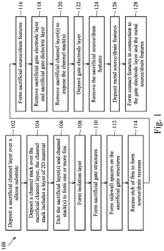
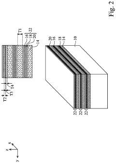
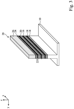
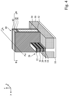
Semiconductor devices including two-dimensional material and methods of fabrication thereof
PatentActiveUS20220384441A1
Innovation
- The use of two-dimensional (2D) material nanosheets as channels in transistors, formed by alternately depositing sacrificial layers and channel stacks, which include a 2D material layer sandwiched between interfacial and high-k dielectric layers, enables higher mobility and reduced dimensions, allowing for increased drive current and integration density.
Regulatory Framework for 2D Semiconductor-Based Medical Devices
The regulatory landscape for 2D semiconductor-based medical devices represents a complex intersection of pharmaceutical regulations, medical device oversight, and emerging technology governance. Currently, these innovative devices fall under multiple regulatory frameworks, including the FDA's Center for Devices and Radiological Health (CDRH) in the United States, the European Medicines Agency's Medical Device Regulation (MDR) in Europe, and similar bodies in other major markets.
Key regulatory considerations include biocompatibility assessment protocols specific to 2D materials, which differ significantly from traditional semiconductor materials. Regulatory bodies are developing specialized testing requirements for these novel interfaces between electronic components and biological systems, with particular emphasis on long-term stability and potential degradation products.
Risk classification frameworks are being adapted to accommodate the unique properties of 2D semiconductor devices. Most regulatory agencies currently classify these as Class III (high-risk) devices due to their novel nature and direct interaction with biological systems, requiring the most stringent approval pathways including Premarket Approval (PMA) in the US context.
Data security and privacy regulations present additional compliance challenges, as many 2D semiconductor-based medical devices incorporate sensing and data transmission capabilities. Manufacturers must navigate HIPAA compliance in the US and GDPR requirements in Europe, implementing robust encryption and data protection measures from the design phase.
International harmonization efforts are underway through the International Medical Device Regulators Forum (IMDRF) to develop consistent approaches to 2D semiconductor technology evaluation. These initiatives aim to reduce regulatory fragmentation while maintaining appropriate safety standards across global markets.
Accelerated approval pathways are emerging for certain applications, particularly in therapeutic areas with significant unmet needs. The FDA's Breakthrough Devices Program and similar expedited review processes in other jurisdictions have begun accepting applications for innovative 2D semiconductor-based diagnostic and therapeutic technologies.
Regulatory science is evolving rapidly in this domain, with collaborative research initiatives between industry, academia, and regulatory bodies focused on developing appropriate testing methodologies and standards. These efforts are critical for establishing evidence-based regulatory frameworks that balance innovation with patient safety considerations.
Post-market surveillance requirements for these devices tend to be particularly rigorous, with extended monitoring periods and comprehensive adverse event reporting systems to capture long-term performance and safety data in real-world clinical settings.
Biocompatibility and Safety Considerations for Clinical Applications
The integration of 2D semiconductors into pharmaceutical applications necessitates rigorous evaluation of biocompatibility and safety profiles. These atomically thin materials, including graphene, transition metal dichalcogenides (TMDs), and hexagonal boron nitride (h-BN), interact with biological systems in unique ways that must be thoroughly understood before clinical implementation.
Biocompatibility assessments for 2D semiconductor-based pharmaceutical technologies follow a multi-tiered approach. In vitro cytotoxicity studies have demonstrated variable results depending on material composition, size, surface functionalization, and concentration. Graphene oxide typically exhibits higher cytotoxicity than pristine graphene, while MoS2 nanosheets show promising biocompatibility profiles at therapeutic concentrations.
Hemocompatibility represents another critical consideration, as 2D materials intended for systemic administration must not induce hemolysis, thrombogenicity, or complement activation. Recent studies indicate that edge-passivated TMDs demonstrate superior hemocompatibility compared to their unmodified counterparts, suggesting potential pathways for safety optimization.
Immunogenicity concerns remain paramount, as foreign materials can trigger immune responses that compromise therapeutic efficacy and patient safety. Surface PEGylation and biomimetic coating strategies have emerged as effective approaches to mitigate immunogenicity while preserving the functional properties of 2D semiconductors in pharmaceutical applications.
Biodegradation and clearance pathways significantly impact the long-term safety profile of 2D semiconductor-based pharmaceuticals. Materials that persist in biological systems pose greater risks for accumulation toxicity. Engineered biodegradable variants of MoS2 and WS2 that decompose under physiological conditions represent promising advances in addressing this challenge.
Regulatory frameworks for 2D semiconductor-based pharmaceuticals remain in development, with the FDA and EMA establishing specialized working groups to address the unique characteristics of these materials. Current guidelines emphasize comprehensive physicochemical characterization, standardized toxicity testing protocols, and detailed biodistribution studies to establish safety profiles.
Translational challenges include batch-to-batch variability in material properties, scalable production of GMP-compliant materials, and development of validated analytical methods for detecting 2D materials in complex biological matrices. Addressing these challenges requires interdisciplinary collaboration between materials scientists, pharmaceutical technologists, toxicologists, and regulatory experts.
Future directions in biocompatibility research focus on establishing structure-activity relationships that predict biological interactions, developing in silico models to screen potential toxicity, and creating standardized reporting frameworks to facilitate cross-study comparisons and accelerate clinical translation of 2D semiconductor-based pharmaceutical technologies.
Unlock deeper insights with Patsnap Eureka Quick Research — get a full tech report to explore trends and direct your research. Try now!
Generate Your Research Report Instantly with AI Agent
Supercharge your innovation with Patsnap Eureka AI Agent Platform!