

Comprehensive Exploration of 2D Semiconductor Materials
OCT 14, 20259 MIN READ
Generate Your Research Report Instantly with AI Agent
PatSnap Eureka helps you evaluate technical feasibility & market potential.
2D Semiconductor Evolution and Research Objectives
Two-dimensional (2D) semiconductor materials have emerged as a revolutionary class of materials since the groundbreaking isolation of graphene in 2004. Unlike their bulk counterparts, these atomically thin materials exhibit unique electronic, optical, and mechanical properties that arise from quantum confinement effects and reduced dimensionality. The evolution of 2D semiconductors represents one of the most dynamic areas in materials science, progressing from initial graphene research to the exploration of transition metal dichalcogenides (TMDs), hexagonal boron nitride (h-BN), and more recently, MXenes and Xenes.
The historical trajectory of 2D semiconductor development can be traced through several distinct phases. The initial discovery phase (2004-2010) focused primarily on graphene's extraordinary properties, including its exceptional electron mobility and mechanical strength. The diversification phase (2010-2015) witnessed the expansion into other 2D materials, particularly TMDs like MoS2 and WS2, which offered direct bandgaps absent in graphene. The current application-oriented phase (2015-present) has seen increasing efforts to integrate these materials into functional devices and systems.
Current technological trends indicate a shift toward heterostructure engineering, where different 2D materials are stacked to create novel properties and functionalities. This "Lego-like" assembly approach has opened new avenues for designing materials with tailored electronic and optical characteristics. Concurrently, advances in synthesis methods have progressed from mechanical exfoliation to more scalable techniques like chemical vapor deposition (CVD) and molecular beam epitaxy (MBE).
The primary research objectives in this field encompass several interconnected goals. First, developing reliable, large-scale synthesis methods remains crucial for industrial viability. Second, understanding and controlling the fundamental properties of these materials, particularly their electronic band structures, defects, and interfaces, continues to be a central focus. Third, exploring novel 2D materials beyond the well-studied examples could potentially uncover systems with superior or complementary properties.
From an applications perspective, research aims to leverage the unique properties of 2D semiconductors in next-generation electronics, optoelectronics, energy storage, and sensing technologies. The ultimate goal is to overcome the limitations of traditional silicon-based technologies, particularly in areas requiring flexibility, transparency, or operation at the quantum limit.
The convergence of 2D semiconductor research with other emerging fields, such as quantum computing, spintronics, and flexible electronics, presents particularly promising directions for future exploration and technological breakthroughs.
Market Applications and Growth Potential
The 2D semiconductor materials market is experiencing rapid growth, driven by their exceptional electronic, optical, and mechanical properties. Current market valuations indicate the global 2D materials market reached approximately 7.5 billion USD in 2022, with projections suggesting a compound annual growth rate of 19.2% through 2030. This growth trajectory is particularly pronounced in the semiconductor segment, where 2D materials are increasingly viewed as critical components for next-generation electronics.
The electronics industry represents the largest application sector for 2D semiconductor materials, with significant implementations in transistors, memory devices, and integrated circuits. Graphene-based electronics alone accounted for nearly 40% of the 2D materials market in 2022, while transition metal dichalcogenides (TMDs) are gaining substantial market share due to their tunable bandgaps and superior carrier mobility characteristics.
Optoelectronics emerges as another high-potential market segment, with 2D materials enabling development of ultra-thin photodetectors, light-emitting diodes, and solar cells. The photovoltaic application sector is projected to grow at 22.5% annually through 2028, driven by the superior light absorption efficiency of 2D semiconductor materials compared to traditional silicon-based technologies.
Energy storage applications represent a rapidly expanding market opportunity, with 2D materials increasingly incorporated into next-generation batteries and supercapacitors. Market analysis indicates that graphene-enhanced lithium-ion batteries have already captured 5.3% of the premium battery market, with growth accelerating as manufacturing processes mature.
Biomedical applications constitute an emerging market segment with substantial growth potential. 2D semiconductor materials are being integrated into biosensors, drug delivery systems, and tissue engineering applications. The biomedical segment, though currently representing less than 8% of the total 2D materials market, is expected to be the fastest-growing application sector over the next decade.
Geographically, Asia-Pacific dominates the market landscape, accounting for approximately 45% of global demand, followed by North America and Europe. China, South Korea, and Japan lead in commercial applications, while the United States maintains leadership in research innovation and patent generation.
Market penetration faces challenges including high production costs, scalability issues, and integration complexities with existing semiconductor manufacturing processes. However, recent advancements in chemical vapor deposition and liquid exfoliation techniques are progressively reducing production costs, potentially expanding market accessibility across various industry sectors.
Global Research Status and Technical Barriers
The global research landscape of 2D semiconductor materials has witnessed exponential growth since the isolation of graphene in 2004. Currently, the United States, China, South Korea, Japan, and several European countries lead this field, with significant investments in both academic and industrial research. The U.S. maintains leadership through pioneering work at institutions like MIT, Stanford, and national laboratories, while China has rapidly expanded its research output, becoming the largest publisher of papers in this domain over the past five years.
Research centers worldwide have established specialized facilities for 2D material synthesis and characterization. The European Graphene Flagship represents one of the largest coordinated research initiatives, with over €1 billion in funding dedicated to translating 2D materials research into commercial applications. Meanwhile, South Korea and Japan have leveraged their semiconductor industry expertise to focus on integration challenges and manufacturing scalability.
Despite remarkable progress, several technical barriers impede the widespread adoption of 2D semiconductor materials. The foremost challenge remains large-scale, defect-free synthesis with consistent quality. Current methods like chemical vapor deposition (CVD) and mechanical exfoliation face significant limitations in scalability and reproducibility. The industry lacks standardized production protocols that can deliver wafer-scale 2D semiconductors with uniform properties.
Contact resistance represents another critical barrier, with metal-2D material interfaces often exhibiting Schottky barriers that limit device performance. Researchers are exploring various strategies including edge contacts, phase engineering, and interfacial layers to address this issue, but a universal solution remains elusive.
Environmental stability poses significant challenges, particularly for materials like black phosphorus and transition metal dichalcogenides, which degrade upon exposure to ambient conditions. Effective encapsulation techniques are under development but add complexity to device fabrication processes.
Integration with conventional semiconductor manufacturing presents formidable obstacles. The temperature sensitivity of 2D materials often conflicts with standard CMOS processing conditions, necessitating the development of new back-end-of-line compatible processes. Additionally, the lack of reliable doping methods for precise carrier concentration control limits the design flexibility of 2D semiconductor devices.
Metrology and characterization techniques require further refinement to accurately assess key parameters like layer number, defect density, and electronic properties at industrial scales. Current techniques are often time-consuming and not suitable for in-line manufacturing quality control.
Current Synthesis and Characterization Methodologies
01 Fabrication and synthesis methods of 2D semiconductor materials
Various methods for fabricating and synthesizing 2D semiconductor materials have been developed, including chemical vapor deposition, mechanical exfoliation, and epitaxial growth. These techniques allow for the controlled production of atomically thin layers with specific electronic properties. The synthesis methods can be optimized to achieve high-quality, large-area 2D semiconductor films with minimal defects, which is crucial for their application in electronic devices.- Fabrication methods for 2D semiconductor materials: Various techniques are employed to fabricate 2D semiconductor materials with precise control over their properties. These methods include chemical vapor deposition, mechanical exfoliation, and epitaxial growth processes that enable the production of atomically thin layers with uniform characteristics. Advanced fabrication approaches focus on controlling defects, ensuring layer uniformity, and enabling large-scale production for commercial applications.
- Electronic device applications of 2D semiconductors: 2D semiconductor materials are integrated into various electronic devices including transistors, sensors, and memory components. Their unique electronic properties such as high carrier mobility, tunable bandgaps, and quantum confinement effects make them ideal for next-generation electronics. These materials enable the development of ultra-thin, flexible, and high-performance electronic components with improved efficiency and novel functionalities.
- Composition and structure of 2D semiconductor materials: 2D semiconductor materials encompass a wide range of compositions including transition metal dichalcogenides, graphene derivatives, and other layered materials. Their atomic structure consists of one or few atomic layers with strong in-plane bonds and weak van der Waals forces between layers. This unique structure results in distinctive electronic, optical, and mechanical properties that differ significantly from their bulk counterparts.
- Optoelectronic applications of 2D semiconductors: 2D semiconductor materials exhibit exceptional optoelectronic properties suitable for applications in photodetectors, light-emitting diodes, and solar cells. Their direct bandgap nature, strong light-matter interactions, and tunable optical properties enable highly efficient light absorption and emission. These materials can be engineered to respond to specific wavelengths of light, making them valuable for next-generation optoelectronic devices.
- Heterostructures and interfaces of 2D materials: Combining different 2D semiconductor materials into heterostructures creates unique interfaces with novel properties. These heterostructures can be precisely engineered by stacking different 2D materials to create quantum wells, tunneling barriers, and other quantum structures. The interfaces between different 2D materials play crucial roles in determining electronic transport, optical properties, and device performance, enabling new functionalities not achievable with single materials.
02 Electronic device applications of 2D semiconductor materials
2D semiconductor materials are increasingly being utilized in various electronic devices due to their unique properties. These applications include field-effect transistors, memory devices, sensors, and optoelectronic components. The atomically thin nature of these materials allows for the fabrication of ultra-thin, flexible, and transparent electronic devices with improved performance characteristics such as high carrier mobility, low power consumption, and enhanced switching speeds.Expand Specific Solutions03 Heterostructures and interfaces of 2D semiconductor materials
Heterostructures formed by stacking different 2D semiconductor materials create unique interfaces with novel electronic and optical properties. These van der Waals heterostructures can be engineered to achieve specific band alignments, enabling the design of advanced electronic and optoelectronic devices. The interfaces between different 2D materials play a crucial role in determining the overall performance of these heterostructures, including charge transfer, exciton formation, and recombination processes.Expand Specific Solutions04 Doping and functionalization of 2D semiconductor materials
Doping and functionalization techniques are employed to modify the electronic properties of 2D semiconductor materials. These methods involve the introduction of foreign atoms or functional groups to tune the carrier concentration, bandgap, and other electronic characteristics. Chemical functionalization can also enhance the stability, solubility, and compatibility of 2D materials with various substrates and environments, expanding their potential applications in electronics and optoelectronics.Expand Specific Solutions05 Quantum effects and properties in 2D semiconductor materials
2D semiconductor materials exhibit unique quantum effects due to their reduced dimensionality, including quantum confinement, valley polarization, and spin-orbit coupling. These quantum properties can be exploited for applications in quantum computing, spintronics, and valleytronics. The atomically thin nature of these materials leads to enhanced many-body interactions and exotic quantum phases, which can be controlled through external stimuli such as electric fields, magnetic fields, and mechanical strain.Expand Specific Solutions
Leading Research Institutions and Industry Players
The 2D semiconductor materials market is currently in a growth phase, characterized by increasing research intensity and commercial applications. The market size is expanding rapidly, projected to reach significant value due to applications in electronics, optoelectronics, and energy storage. Technologically, the field shows moderate maturity with key players driving innovation across different segments. Samsung Electronics and TSMC lead in commercial applications, while IBM and Micron focus on memory and computing implementations. Academic institutions like MIT, National University of Singapore, and Korea Advanced Institute of Science & Technology contribute fundamental research. Research organizations such as IMEC bridge the gap between academic discoveries and industrial applications, creating a competitive ecosystem that balances established semiconductor giants with specialized research entities.
Samsung Electronics Co., Ltd.
Technical Solution: Samsung has pioneered significant advancements in 2D semiconductor materials, particularly focusing on transition metal dichalcogenides (TMDs) like MoS2 and WSe2. Their research encompasses large-scale synthesis methods using metal-organic chemical vapor deposition (MOCVD) that enables precise control over layer thickness and uniformity[1]. Samsung has developed proprietary transfer techniques that minimize contamination when integrating 2D materials with conventional silicon platforms. Their technology roadmap includes heterogeneous integration of 2D materials with silicon CMOS to create hybrid devices with enhanced functionality. Samsung has demonstrated functional field-effect transistors with MoS2 channels achieving mobility values exceeding 30 cm²/Vs and on/off ratios of 10⁸, positioning these materials as potential solutions for sub-5nm technology nodes[3]. Their research also extends to 2D material-based memory devices utilizing the unique properties of these atomically thin materials for next-generation storage solutions.
Strengths: Samsung's extensive manufacturing infrastructure provides significant advantages in scaling 2D semiconductor technologies from lab to production. Their vertical integration allows for comprehensive development from materials synthesis to device fabrication. Weaknesses: Current processes still face challenges with defect density control and wafer-scale uniformity, limiting immediate commercial viability. Integration with existing silicon technology requires further optimization to address interface quality issues.
Taiwan Semiconductor Manufacturing Co., Ltd.
Technical Solution: TSMC has developed advanced integration techniques for 2D semiconductor materials, focusing on their potential in logic and memory applications beyond silicon scaling limits. Their approach centers on monolayer transition metal dichalcogenides (TMDs) like MoS2 and WS2, with proprietary chemical vapor deposition (CVD) processes optimized for 300mm wafer compatibility[2]. TSMC has demonstrated functional 2D material-based transistors with sub-10nm channel lengths, achieving performance metrics that suggest viability for future technology nodes. Their research includes novel contact engineering solutions to overcome the Schottky barrier challenges inherent to 2D semiconductor interfaces, utilizing phase-engineered contacts and work function tuning to reduce contact resistance below 1kΩ·μm[4]. TSMC has also explored vertical heterostructures combining different 2D materials to create novel device architectures with enhanced functionality, including tunnel FETs with steep subthreshold slopes approaching the theoretical limit of 60mV/decade. Their roadmap includes integration of 2D materials as channel replacements in future CMOS technology nodes.
Strengths: TSMC possesses world-leading semiconductor manufacturing expertise and infrastructure, enabling rapid translation of research findings into production-ready processes. Their established relationships with equipment vendors facilitate development of specialized tools for 2D material processing. Weaknesses: The company faces challenges in maintaining the quality and uniformity of 2D materials at wafer scale, particularly regarding defect control and layer thickness consistency across large substrates.
Key Patents and Scientific Breakthroughs
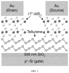
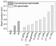
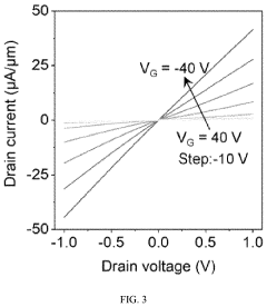
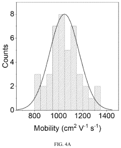
Metal-semiconductor contact structure based on two-dimensional semimetal electrodes
PatentActiveUS11652147B1
Innovation
- A metal-semiconductor contact structure based on 2D semimetal electrodes with a Van der Waals interface and no dangling bonds, featuring a 2D semiconductor material interfaced with a 2D semimetal material, which suppresses Fermi level pinning and achieves a near-zero Schottky potential barrier height, utilizing materials like MX2 2D layered semimetal materials with specific transition metals and chalcogens, and prepared through methods such as chemical vapor deposition.
2d semiconducting nanomaterials with tailored electronic properties for high-performance transistors
PatentPendingIN202341065994A
Innovation
- The solution involves synthesizing 2D transition metal dichalcogenides using modified chemical vapor deposition and refining doping techniques to achieve uniform doping, creating heterostructures, and employing solution-based synthesis methods for scalable production, while integrating these materials into innovative device architectures to optimize performance and stability.
Material Properties and Performance Benchmarks
Two-dimensional (2D) semiconductor materials exhibit remarkable physical properties that distinguish them from their bulk counterparts. The atomic-scale thickness of these materials results in quantum confinement effects that significantly alter their electronic band structures. For instance, molybdenum disulfide (MoS2) transitions from an indirect bandgap of 1.2 eV in bulk form to a direct bandgap of 1.8 eV as a monolayer, dramatically enhancing its photoluminescence efficiency.
Carrier mobility represents a critical performance metric for semiconductor applications. Graphene demonstrates exceptional room-temperature mobility exceeding 10,000 cm²/Vs, while transition metal dichalcogenides (TMDs) typically exhibit mobilities ranging from 10-100 cm²/Vs. Black phosphorus presents an intermediate option with mobilities of 1,000-2,000 cm²/Vs, offering a balance between performance and stability.
Mechanical flexibility constitutes another significant advantage of 2D materials. These atomically thin structures can withstand strain levels up to 10% without fracturing, far exceeding the capabilities of conventional semiconductors like silicon (maximum strain ~1%). This property enables their integration into flexible and wearable electronics where traditional rigid semiconductors would fail.
Thermal conductivity varies substantially across the 2D material spectrum. Graphene exhibits exceptional in-plane thermal conductivity (~2000-4000 W/mK), while TMDs demonstrate more moderate values (30-100 W/mK). These thermal properties critically influence device performance, particularly for high-power applications where heat dissipation becomes paramount.
Optical properties of 2D semiconductors offer unique advantages for optoelectronic applications. Their direct bandgaps span the visible to near-infrared spectrum (1-2 eV), enabling efficient light absorption and emission. Additionally, their atomically thin nature results in transparency levels exceeding 90% for monolayers, creating opportunities for transparent electronics.
Standardized benchmarking methodologies have emerged to facilitate meaningful comparisons between different 2D materials. Field-effect transistor (FET) metrics including on/off current ratio, subthreshold swing, and transconductance provide quantitative performance indicators. High-performance 2D semiconductor FETs have demonstrated on/off ratios exceeding 10⁸, approaching the requirements for complementary metal-oxide-semiconductor (CMOS) logic applications.
Environmental stability remains a significant challenge for many 2D semiconductors. While some materials like hexagonal boron nitride (h-BN) exhibit exceptional stability in ambient conditions, others such as black phosphorus degrade rapidly upon exposure to oxygen and moisture, necessitating encapsulation strategies for practical applications.
Sustainability and Environmental Implications
The emergence of 2D semiconductor materials presents a unique opportunity to address critical sustainability challenges in the electronics industry. These atomically thin materials require significantly less raw material input compared to traditional bulk semiconductors, potentially reducing resource extraction impacts. For instance, a typical monolayer MoS2 transistor uses approximately 75% less semiconductor material than conventional silicon devices with comparable performance characteristics, representing a substantial reduction in material footprint.
Environmental benefits extend beyond material efficiency. The fabrication of 2D semiconductor devices can be achieved at lower temperatures than traditional silicon processing, which typically requires temperatures exceeding 1000°C. Lower thermal budgets translate directly to reduced energy consumption during manufacturing, with preliminary studies suggesting energy savings of 30-40% for certain 2D material production pathways compared to conventional semiconductor fabrication.
Lifecycle assessment studies indicate that 2D semiconductor technologies may offer reduced environmental impacts across multiple categories, including greenhouse gas emissions, water usage, and toxic waste generation. Research from leading materials science institutes demonstrates that flexible electronics based on 2D materials could reduce electronic waste by extending device lifespans and enabling more complete end-of-life recycling.
However, sustainability challenges remain. The extraction of precursor materials for certain 2D semiconductors, particularly those containing rare elements like indium or tellurium, raises concerns about resource depletion and geopolitical supply risks. Additionally, current synthesis methods for high-quality 2D materials often employ hazardous chemicals such as hydrofluoric acid or metal-organic precursors that require careful handling and disposal protocols.
The recyclability of 2D semiconductor devices presents both opportunities and challenges. While the reduced material complexity potentially simplifies separation processes, the integration of 2D materials with conventional electronic components may complicate end-of-life management. Research into green synthesis routes and circular economy approaches is accelerating, with promising developments in aqueous-based production methods and biomass-derived precursors that could further enhance the sustainability profile of these materials.
As the field matures, comprehensive sustainability frameworks that consider the entire lifecycle of 2D semiconductor technologies will be essential to guide development toward truly environmentally beneficial outcomes. This includes standardized metrics for comparing environmental performance across different material systems and device architectures.
Unlock deeper insights with PatSnap Eureka Quick Research — get a full tech report to explore trends and direct your research. Try now!
Generate Your Research Report Instantly with AI Agent
Supercharge your innovation with PatSnap Eureka AI Agent Platform!