

Performance Comparison: 2D vs Conventional Semiconductors
OCT 14, 20259 MIN READ
Generate Your Research Report Instantly with AI Agent
PatSnap Eureka helps you evaluate technical feasibility & market potential.
2D Semiconductors Background and Objectives
Two-dimensional (2D) semiconductors represent a revolutionary class of materials that have emerged as potential successors to conventional three-dimensional semiconductors in various electronic applications. Since the isolation of graphene in 2004, the field has expanded dramatically to include transition metal dichalcogenides (TMDs), hexagonal boron nitride (h-BN), and other layered materials with atomic-scale thickness. These materials exhibit unique physical properties when reduced to monolayer or few-layer forms, creating new possibilities for next-generation electronics.
The evolution of semiconductor technology has historically been driven by Moore's Law, which predicted the doubling of transistor density approximately every two years. However, conventional silicon-based semiconductors are approaching fundamental physical limits in terms of miniaturization and performance enhancement. This technological bottleneck has accelerated research into alternative materials that can overcome these limitations while enabling new functionalities.
2D semiconductors offer several intrinsic advantages over their bulk counterparts. Their atomically thin nature provides excellent electrostatic control, potentially allowing for more efficient field-effect transistors with reduced short-channel effects. Many 2D materials also exhibit direct bandgaps in their monolayer form, unlike their bulk counterparts, enabling more efficient light emission and absorption for optoelectronic applications.
The primary objective of investigating 2D semiconductors is to determine whether they can outperform conventional semiconductors in specific application domains. This includes evaluating their potential for ultra-scaled logic devices, flexible electronics, sensors, and energy conversion systems. Additionally, research aims to understand how the unique quantum confinement effects in these materials can be harnessed for novel device architectures that transcend traditional semiconductor capabilities.
Current technical goals include improving carrier mobility in 2D materials, which often suffers from scattering mechanisms at interfaces and defects. Developing reliable methods for large-area synthesis with consistent quality remains another critical challenge. Furthermore, establishing techniques for precise control of layer number, doping, and contact engineering is essential for practical device implementation.
The trajectory of 2D semiconductor development is increasingly focused on heterostructures—combinations of different 2D materials stacked with atomic precision—which offer unprecedented freedom in band structure engineering. These "van der Waals heterostructures" represent a paradigm shift in material design, allowing for the creation of artificial materials with tailored electronic properties not found in nature.
As the field matures, research is expanding beyond individual device performance to address system-level integration challenges and explore new computing paradigms that leverage the unique properties of 2D materials, including neuromorphic computing and quantum information processing.
Market Analysis for 2D Semiconductor Applications
The 2D semiconductor market is experiencing rapid growth, projected to reach $5.7 billion by 2030, with a compound annual growth rate of approximately 19% from 2023. This growth is primarily driven by the increasing demand for miniaturized electronic devices with enhanced performance capabilities. The transition from conventional 3D semiconductors to 2D materials represents a significant shift in the semiconductor industry, addressing the limitations of traditional silicon-based technologies as they approach their physical scaling limits.
Key application sectors for 2D semiconductors include consumer electronics, telecommunications, automotive, and healthcare. In consumer electronics, 2D semiconductors enable the development of flexible displays, wearable devices, and ultra-thin smartphones. The telecommunications sector benefits from 2D materials in high-frequency electronics and next-generation communication systems, particularly for 5G and future 6G networks where conventional semiconductors struggle to meet performance requirements.
The automotive industry is increasingly adopting 2D semiconductors for advanced driver-assistance systems (ADAS), autonomous driving technologies, and electric vehicle components. These materials offer advantages in power efficiency, thermal management, and reliability under extreme conditions. In healthcare, 2D semiconductors are finding applications in biosensors, medical imaging devices, and point-of-care diagnostic tools.
Regional market analysis indicates that Asia-Pacific currently dominates the 2D semiconductor market, with significant investments from countries like China, South Korea, and Japan. North America follows closely, driven by research initiatives and technology startups, particularly in the United States. Europe is also emerging as a competitive region, with strong focus on research and development in countries like Germany and the United Kingdom.
Market challenges include high production costs, scalability issues, and integration complexities with existing semiconductor manufacturing processes. Despite these challenges, the unique properties of 2D semiconductors—such as superior electron mobility, flexibility, and optical transparency—continue to drive market expansion.
Investor interest in 2D semiconductor technologies has grown substantially, with venture capital funding increasing by 45% in the past three years. Major semiconductor manufacturers are establishing dedicated research divisions or acquiring startups specializing in 2D materials, indicating strong confidence in the market's future potential.
Customer demand patterns show increasing preference for devices with longer battery life, faster processing speeds, and reduced form factors—all advantages offered by 2D semiconductor technologies compared to conventional alternatives. This alignment between 2D semiconductor capabilities and evolving consumer expectations suggests sustained market growth in the coming decade.
Technical Challenges in 2D vs Conventional Semiconductors
Despite significant advancements in conventional semiconductor technology, fundamental physical limitations are increasingly constraining further performance improvements. Silicon-based devices face challenges with quantum tunneling effects when transistor dimensions approach sub-10nm scales, resulting in increased leakage currents and power consumption. Heat dissipation has become a critical bottleneck, with thermal management systems struggling to maintain optimal operating temperatures in high-performance applications.
2D semiconductors present their own unique set of technical challenges. Material synthesis remains problematic, with large-scale production of high-quality, defect-free 2D materials still difficult to achieve consistently. Current chemical vapor deposition (CVD) and mechanical exfoliation methods produce materials with varying quality and limited scalability, hampering industrial adoption. Additionally, the integration of 2D materials with existing silicon-based fabrication processes presents significant compatibility issues.
Contact resistance at metal-2D semiconductor interfaces represents another major obstacle. The atomically thin nature of 2D materials creates unusual contact physics that often results in Schottky barriers and high contact resistance, degrading device performance. This challenge is particularly pronounced in molybdenum disulfide (MoS2) and other transition metal dichalcogenides (TMDs).
Environmental stability poses concerns for 2D semiconductor implementation. Many promising 2D materials exhibit performance degradation when exposed to ambient conditions, with oxidation and moisture sensitivity affecting long-term reliability. Encapsulation techniques add complexity and cost to manufacturing processes while potentially limiting performance benefits.
The bandgap engineering of 2D materials presents both opportunities and challenges. While the ability to tune electronic properties through layer count, strain, and composition offers unprecedented flexibility, precisely controlling these parameters at industrial scales remains technically demanding. The relationship between structural modifications and resulting electronic properties is not yet fully predictable or controllable.
Metrology and characterization tools optimized for conventional semiconductors often prove inadequate for 2D materials. The atomically thin nature of these materials requires specialized techniques for defect analysis, layer counting, and performance evaluation. This gap in measurement capabilities slows research progress and manufacturing quality control.
Device architecture optimization represents a significant challenge in transitioning from conventional to 2D semiconductors. Traditional MOSFET designs may not fully leverage the unique properties of 2D materials, necessitating novel device structures. Gate control, channel engineering, and dielectric integration all require fundamental rethinking when working with atomically thin materials.
Current Performance Comparison Methodologies
01 Performance comparison between 2D and conventional semiconductors
2D semiconductors offer unique performance advantages over conventional 3D semiconductors, including superior carrier mobility, reduced short-channel effects, and better electrostatic control. These materials, typically only a few atoms thick, demonstrate exceptional electrical properties that can overcome limitations faced by traditional silicon-based devices as they approach physical scaling limits. The atomically thin nature of 2D materials enables more efficient gate control and reduced leakage current.- Performance comparison between 2D and conventional semiconductors: 2D semiconductors offer unique performance advantages over conventional semiconductors, including enhanced carrier mobility, reduced short-channel effects, and improved electrostatic control. These materials, typically only a few atoms thick, demonstrate superior electrical properties at nanoscale dimensions where traditional semiconductors face physical limitations. The atomic thinness of 2D materials enables better gate control and reduced leakage current, making them promising candidates for next-generation electronic devices.
- Integration of 2D materials with conventional semiconductor technology: The integration of 2D materials with conventional semiconductor technology presents both challenges and opportunities. Hybrid structures combining 2D semiconductors with traditional silicon-based platforms can leverage the advantages of both material systems. This approach enables novel device architectures that benefit from the established manufacturing infrastructure while incorporating the unique properties of 2D materials. Key integration issues include contact resistance, interface quality, and thermal management that must be addressed for successful commercialization.
- Quantum effects and performance enhancement in 2D semiconductor devices: 2D semiconductor materials exhibit pronounced quantum effects that can be harnessed for performance enhancement. These quantum phenomena, including quantum confinement and tunneling, become dominant at the atomic thickness scale and can be engineered to create devices with novel functionalities. The ability to precisely control quantum states in 2D materials enables improved switching characteristics, reduced power consumption, and potential applications in quantum computing and information processing.
- Thermal and mechanical performance considerations in 2D semiconductor devices: Thermal management and mechanical stability are critical factors affecting the performance of 2D semiconductor devices. The unique thermal conductivity properties of 2D materials can both enhance and limit device performance depending on application requirements. Additionally, the mechanical flexibility of many 2D materials enables applications in flexible and stretchable electronics that are not feasible with conventional rigid semiconductors. Understanding and optimizing these thermal and mechanical characteristics is essential for reliable device operation.
- Advanced manufacturing techniques for 2D semiconductor devices: Novel manufacturing techniques are being developed to overcome the challenges in producing high-quality 2D semiconductor devices at scale. These include specialized growth methods, transfer processes, and patterning techniques that preserve the intrinsic properties of 2D materials. Innovations in fabrication technology are critical for transitioning 2D semiconductor devices from laboratory demonstrations to commercial products. Recent advances focus on reducing defects, improving uniformity, and enhancing compatibility with existing semiconductor manufacturing infrastructure.
02 Integration of 2D materials with conventional semiconductor technology
Hybrid integration approaches combining 2D materials with conventional semiconductor platforms enable novel device architectures that leverage the advantages of both material systems. These integration methods include direct growth or transfer of 2D materials onto silicon substrates, creating heterojunctions with unique electrical properties. Such hybrid systems can enhance performance in applications like memory, logic circuits, and sensors while maintaining compatibility with existing semiconductor manufacturing infrastructure.Expand Specific Solutions03 Quantum effects and band structure engineering in 2D semiconductors
2D semiconductors exhibit pronounced quantum confinement effects that significantly alter their electronic band structures compared to conventional semiconductors. This enables precise band gap engineering through layer number control, strain application, or formation of van der Waals heterostructures. The ability to tune electronic properties at the atomic scale allows for customized performance characteristics that can be optimized for specific applications, offering advantages in optoelectronic devices and quantum computing.Expand Specific Solutions04 Thermal and mechanical performance considerations
The thermal and mechanical properties of 2D semiconductors differ significantly from conventional semiconductors, affecting device performance and reliability. While 2D materials often have lower thermal conductivity than bulk semiconductors, their mechanical flexibility enables applications in bendable and stretchable electronics. Managing heat dissipation in 2D semiconductor devices requires novel thermal interface materials and cooling strategies to prevent performance degradation under high-power operation.Expand Specific Solutions05 Manufacturing challenges and scalability comparison
The manufacturing processes for 2D semiconductors present unique challenges compared to well-established conventional semiconductor fabrication. While conventional semiconductors benefit from decades of manufacturing optimization, 2D materials often require specialized growth techniques like chemical vapor deposition or mechanical exfoliation. Achieving consistent quality, large-area production, and precise control over layer numbers remains challenging for 2D materials, affecting their commercial viability despite their superior performance characteristics in laboratory settings.Expand Specific Solutions
Key Industry Players in 2D Semiconductor Development
The 2D semiconductor market is in an early growth phase, showing significant potential compared to conventional semiconductors due to superior performance characteristics including higher electron mobility and reduced power consumption. The global market is expanding rapidly, driven by applications in electronics, computing, and communications. Leading players like Samsung Electronics, TSMC, and Intel are investing heavily in 2D semiconductor R&D, with Samsung and TSMC focusing on manufacturing process optimization while Intel explores integration with existing silicon technologies. Companies such as Applied Materials and Tokyo Electron are developing specialized equipment for 2D material fabrication. Though still facing commercialization challenges, collaborative efforts between established semiconductor giants and research institutions are accelerating technology maturation, positioning 2D semiconductors as a promising next-generation technology.
Samsung Electronics Co., Ltd.
Technical Solution: Samsung has developed comprehensive comparison frameworks between 2D and conventional semiconductor technologies. Their research focuses on transition metal dichalcogenides (TMDs) as promising 2D semiconductor materials, particularly MoS2 and WSe2, which demonstrate channel lengths below 5nm - significantly outperforming silicon's scaling limits. Samsung's Advanced Institute of Technology has demonstrated functional 2D semiconductor transistors with mobility values exceeding 100 cm²/Vs and on/off ratios greater than 10⁸, addressing key performance metrics that conventional semiconductors struggle to achieve at advanced nodes. Their 2D semiconductor integration approach includes proprietary growth methods for large-area synthesis and transfer techniques that maintain material integrity. Samsung has also pioneered vertical integration of 2D materials with conventional CMOS technology, creating hybrid devices that leverage the advantages of both technologies while maintaining manufacturing compatibility with existing fab infrastructure.
Strengths: Exceptional carrier transport properties in ultra-thin channels; significantly reduced short-channel effects compared to silicon; potential for transparent and flexible electronics applications. Weaknesses: Challenges with contact resistance at metal-2D material interfaces; difficulty achieving uniform material quality across large wafers; thermal management issues in high-performance applications.
Taiwan Semiconductor Manufacturing Co., Ltd.
Technical Solution: TSMC has pioneered advanced semiconductor manufacturing technologies comparing 2D and conventional semiconductors. Their N3E process technology represents their cutting-edge 2D semiconductor approach, delivering approximately 18% speed improvement at the same power or 34% power reduction at the same speed compared to N5 technology. TSMC has also developed ultra-thin 2D semiconductor materials like molybdenum disulfide (MoS2) with atomic-level thickness that enables superior electrostatic control and reduced short-channel effects. Their research shows 2D semiconductors can achieve sub-1nm channel thickness while maintaining high carrier mobility, which is impossible with conventional 3D silicon. TSMC's advanced packaging technologies like InFO (Integrated Fan-Out) and CoWoS (Chip on Wafer on Substrate) specifically optimize 2D semiconductor integration, allowing for heterogeneous integration of different semiconductor technologies.
Strengths: Superior scaling capabilities with atomic-level thickness enabling continued Moore's Law progression; excellent electrostatic control reducing leakage current; potential for flexible electronics applications. Weaknesses: Manufacturing challenges with consistent large-scale production of 2D materials; higher initial production costs compared to mature silicon processes; integration challenges with existing semiconductor infrastructure.
Critical Patents and Research in 2D Semiconductor Field
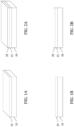
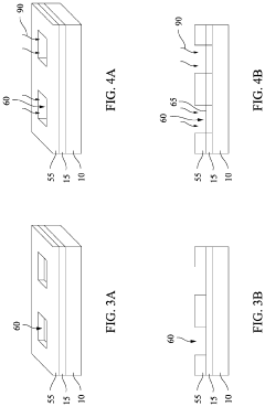
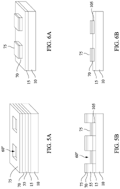
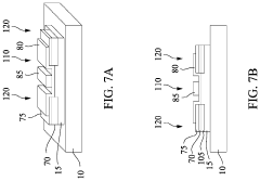
Semiconductor device and method of manufacturing semiconductor device
PatentActiveUS11923203B2
Innovation
- A method is developed to form a metal-reactive metal alloy interface between the semiconductor material and electrical contacts, eliminating the van der Waals gap and reducing contact resistance by using a hydrogen plasma to replace chalcogen in the metal dichalcogenide layer with hydrogen, followed by a reactive metal to form a seamless alloy bond, and a protective less reactive metal layer to prevent oxidation.
Semiconductor device, semiconductor package including the semiconductor device, and method of manufacturing the semiconductor device
PatentPendingUS20250201744A1
Innovation
- The semiconductor device comprises a first semiconductor chip of a first type and a second semiconductor chip of a second type, both with rectangular shapes of the same size. These chips are arranged adjacent to each other in a specific direction, with a mirror-symmetrical structure with respect to an axis perpendicular to that direction, and are alternately stacked on a package substrate.


Manufacturing Scalability Assessment
The manufacturing scalability of 2D semiconductors compared to conventional semiconductors represents a critical factor in their potential for widespread industrial adoption. Currently, conventional silicon-based semiconductor manufacturing has achieved remarkable economies of scale through decades of process optimization, with 300mm wafers being the industry standard and 450mm wafers under development. These established processes enable high-volume production with predictable yields and quality control.
In contrast, 2D semiconductor manufacturing faces significant scalability challenges. The production of high-quality, large-area 2D materials remains difficult to achieve consistently. Methods such as chemical vapor deposition (CVD) and molecular beam epitaxy (MBE) can produce research-grade 2D materials but struggle with uniformity across large substrates. The typical production area for high-quality 2D materials ranges from several square millimeters to a few square centimeters, far below the requirements for commercial semiconductor manufacturing.
Transfer processes present another major hurdle for 2D semiconductor scalability. Most 2D materials are grown on substrates different from those used in device fabrication, necessitating transfer steps that can introduce defects, contamination, and yield loss. While roll-to-roll transfer techniques show promise for large-scale production, they currently lack the precision required for advanced semiconductor applications.
Equipment compatibility also impacts manufacturing scalability. Conventional semiconductor fabs utilize highly specialized equipment optimized for silicon processing. Adapting these tools for 2D materials often requires significant modifications or entirely new equipment development, representing substantial capital investment barriers for manufacturers considering 2D semiconductor adoption.
Integration with existing CMOS processes presents both challenges and opportunities. The relatively low thermal budgets required for many 2D materials (typically below 400°C) make them potentially compatible with back-end-of-line processes, enabling novel 3D integration schemes. However, this integration demands careful process development to avoid compromising either the 2D materials or the underlying CMOS structures.
Cost considerations remain paramount in manufacturing scalability assessment. While 2D semiconductors offer theoretical advantages in material efficiency (being atomically thin), the current production costs significantly exceed those of conventional semiconductors due to low yields, specialized equipment requirements, and process complexity. Industry analysts estimate that production costs need to decrease by at least an order of magnitude to achieve competitive pricing with conventional semiconductor technologies.
Environmental Impact and Sustainability Considerations
The environmental footprint of semiconductor manufacturing represents a critical consideration in the ongoing transition from conventional 3D semiconductors to emerging 2D materials. Traditional semiconductor fabrication processes are notoriously resource-intensive, requiring substantial amounts of ultra-pure water, specialized chemicals, and energy. Silicon-based manufacturing typically consumes between 2,000 to 4,000 liters of water per wafer, creating significant environmental pressure in water-stressed regions where manufacturing facilities are often located.
2D semiconductors offer promising environmental advantages through potentially streamlined production processes. Materials like graphene, molybdenum disulfide (MoS2), and hexagonal boron nitride (h-BN) can be produced using less energy-intensive methods such as chemical vapor deposition and mechanical exfoliation. Research indicates that fully optimized 2D semiconductor production could reduce energy consumption by up to 30-45% compared to conventional silicon manufacturing, primarily due to lower processing temperatures and fewer fabrication steps.
Waste generation represents another significant environmental concern in semiconductor manufacturing. Conventional processes generate hazardous byproducts including perfluorinated compounds, heavy metals, and acidic waste streams. 2D semiconductor production potentially reduces these environmental hazards through decreased chemical usage and the elimination of certain etching processes. However, challenges remain in scaling production while maintaining these environmental benefits.
The lifecycle carbon footprint comparison between 2D and conventional semiconductors reveals complex tradeoffs. While 2D materials may require less energy during manufacturing, the current small-scale production methods can be carbon-intensive per unit of output. As manufacturing scales, this balance is expected to shift favorably toward 2D materials, with preliminary lifecycle assessments suggesting potential carbon footprint reductions of 15-25% at industrial scale.
Resource efficiency extends beyond manufacturing to device performance. 2D semiconductors' superior electron mobility and thermal properties enable more energy-efficient electronic devices, potentially reducing operational energy consumption by 10-30% compared to conventional semiconductor-based devices. This operational efficiency represents a significant sustainability advantage over the product lifecycle.
End-of-life considerations also favor 2D materials in certain applications. Their atomically thin nature requires significantly less material input, potentially reducing mining impacts and associated environmental degradation. Additionally, some 2D materials show promising recyclability characteristics, though commercial-scale recycling processes remain underdeveloped and require further research investment.
Unlock deeper insights with PatSnap Eureka Quick Research — get a full tech report to explore trends and direct your research. Try now!
Generate Your Research Report Instantly with AI Agent
Supercharge your innovation with PatSnap Eureka AI Agent Platform!