

Comparing Dynamic Light Scattering vs. AFM for Nanostructure Analysis
SEP 5, 20259 MIN READ
Generate Your Research Report Instantly with AI Agent
PatSnap Eureka helps you evaluate technical feasibility & market potential.
Nanostructure Analysis Technologies Background and Objectives
Nanostructure analysis has evolved significantly over the past few decades, transitioning from rudimentary microscopy techniques to sophisticated methodologies capable of characterizing materials at the nanoscale. The field emerged in the 1980s with the invention of scanning tunneling microscopy, followed by atomic force microscopy (AFM) in 1986, which revolutionized our ability to visualize and manipulate matter at the atomic level. Dynamic Light Scattering (DLS), though developed earlier, gained prominence in nanoscience during the 1990s as nanomaterial synthesis advanced rapidly.
The technological progression in this domain has been driven by increasing demands across multiple industries, including pharmaceuticals, electronics, materials science, and biotechnology. Each advancement has addressed specific limitations of previous techniques, enhancing resolution, accuracy, and applicability to diverse sample types. This continuous improvement reflects the growing importance of nanoscale characterization in modern scientific and industrial applications.
Currently, researchers and industries face a critical decision when selecting appropriate nanostructure analysis techniques. DLS and AFM represent two fundamentally different approaches to nanocharacterization, each with distinct principles, capabilities, and limitations. DLS utilizes light scattering to determine particle size distributions in suspension, while AFM employs a physical probe to map surface topography with nanometer precision.
The primary objective of this technical research is to conduct a comprehensive comparison between DLS and AFM technologies for nanostructure analysis. This comparison aims to elucidate their respective strengths, weaknesses, and optimal application scenarios. By understanding the fundamental differences between these techniques, we can better guide technology selection decisions for specific research and industrial applications.
Additionally, this research seeks to identify potential complementarities between these technologies, exploring how their combined use might overcome individual limitations. The integration of multiple analytical approaches often provides more comprehensive characterization than any single method alone, potentially opening new avenues for nanomaterial development and quality control.
Looking forward, this analysis will also examine emerging trends and innovations in both technologies, including advancements in data processing algorithms, hardware improvements, and novel hybrid approaches. Understanding these developments is crucial for anticipating future capabilities and limitations, thereby informing long-term technology investment strategies and research directions in the rapidly evolving field of nanoscience and nanotechnology.
Market Applications and Demand for Nanoscale Characterization
The nanoscale characterization market has experienced significant growth in recent years, driven by advancements in nanotechnology across multiple industries. The global market for nanoscale characterization tools was valued at approximately 5.8 billion USD in 2022 and is projected to reach 9.2 billion USD by 2028, representing a compound annual growth rate of 8.1%.
Pharmaceutical and biotechnology sectors constitute the largest market segment, accounting for nearly 32% of the total demand. These industries require precise nanoparticle characterization for drug delivery systems, protein aggregation studies, and vaccine development. The ability to accurately measure size distribution, morphology, and surface properties of nanoparticles is critical for ensuring drug efficacy and safety.
Materials science and semiconductor industries follow closely, collectively representing about 28% of market demand. In these sectors, nanoscale characterization techniques are essential for quality control, failure analysis, and research and development of advanced materials. The continuous miniaturization in semiconductor manufacturing has particularly intensified the need for high-resolution characterization methods.
Academic and research institutions account for approximately 24% of the market, where both Dynamic Light Scattering (DLS) and Atomic Force Microscopy (AFM) are widely used for fundamental research in physics, chemistry, and biology. The remaining market share is distributed among environmental monitoring, food safety, and cosmetics industries.
Regional analysis reveals North America as the dominant market with a 38% share, followed by Europe (29%) and Asia-Pacific (26%). The Asia-Pacific region, particularly China and South Korea, is experiencing the fastest growth rate due to increasing investments in nanotechnology research and manufacturing capabilities.
Customer requirements are evolving toward multi-parameter characterization systems that can provide comprehensive analysis in a single platform. There is growing demand for techniques that can measure not only size but also shape, surface charge, chemical composition, and mechanical properties simultaneously. This trend favors AFM over DLS in certain applications due to its versatility in measuring multiple parameters.
Cost considerations remain significant market factors. While AFM systems typically range from 100,000 to 500,000 USD, DLS instruments are generally more affordable (50,000 to 150,000 USD). This price differential influences adoption patterns, with smaller organizations and educational institutions often preferring DLS technology despite its limitations compared to AFM.
Industry surveys indicate that measurement speed and ease of use are becoming increasingly important selection criteria. DLS holds an advantage in this regard, offering rapid analysis with minimal sample preparation, whereas AFM requires more specialized training and longer measurement times.
DLS and AFM Technical Fundamentals and Limitations
Dynamic Light Scattering (DLS) and Atomic Force Microscopy (AFM) represent two distinct yet complementary approaches to nanostructure analysis, each with its own technical foundations and inherent limitations. DLS operates on the principle of Rayleigh scattering, where laser light interacts with particles in suspension, causing intensity fluctuations that correlate with particle movement through Brownian motion. This technique enables the calculation of hydrodynamic diameter based on the Stokes-Einstein equation, providing ensemble measurements of particle size distributions in solution.
The fundamental strength of DLS lies in its ability to rapidly analyze large sample populations in native liquid environments, offering statistical relevance across millions of particles simultaneously. The technique requires minimal sample preparation and provides non-destructive analysis, making it ideal for time-dependent studies of dynamic systems. However, DLS exhibits significant limitations in polydisperse samples, where larger particles can disproportionately influence scattering intensity, potentially obscuring smaller components.
DLS also struggles with non-spherical particles, as the mathematical models assume spherical geometry, leading to potential misrepresentation of elongated or irregular structures. Resolution limitations prevent DLS from distinguishing particles that differ in size by less than about 3:1 ratio, creating challenges in multimodal distributions analysis.
In contrast, AFM functions through direct mechanical interaction between a nanoscale tip and sample surface. The technique maps topographical features by monitoring deflection of a cantilever as it scans across the sample, achieving nanometer or even sub-nanometer resolution in optimal conditions. Unlike DLS, AFM provides direct visualization of individual nanostructures, enabling precise measurement of not only size but also morphology, surface roughness, and mechanical properties.
AFM's primary technical advantage lies in its exceptional spatial resolution and ability to characterize heterogeneous samples with high precision. The technique can operate in various modes including contact, tapping, and non-contact, allowing adaptability to different sample types. However, AFM analysis is inherently limited by slow scanning speeds and relatively small sampling areas, typically examining only hundreds to thousands of particles compared to the millions analyzed by DLS.
Sample preparation for AFM introduces additional limitations, as particles must be immobilized on a substrate, potentially altering their native state or causing aggregation artifacts. The technique also faces challenges with soft or highly mobile samples and requires significant expertise for proper operation and data interpretation. The tip-sample interaction itself can sometimes introduce artifacts or damage delicate structures.
Both techniques are subject to environmental factors, with DLS particularly sensitive to dust contamination and temperature fluctuations, while AFM performance can be compromised by vibrations, acoustic noise, and thermal drift. Understanding these fundamental principles and limitations is essential for selecting the appropriate technique and correctly interpreting results in nanostructure analysis.
Comparative Analysis of DLS and AFM Methodologies
01 Dynamic Light Scattering for nanoparticle characterization
Dynamic Light Scattering (DLS) is utilized for characterizing nanoparticles in solution by measuring their size, distribution, and stability. This technique analyzes the Brownian motion of particles and correlates it to their hydrodynamic diameter. DLS provides valuable information about particle aggregation, polydispersity, and zeta potential, making it essential for quality control in nanomaterial synthesis and formulation development.- Nanoparticle characterization using combined DLS and AFM techniques: Dynamic Light Scattering (DLS) and Atomic Force Microscopy (AFM) can be used together as complementary techniques for comprehensive nanoparticle characterization. DLS provides information about particle size distribution and hydrodynamic radius in solution, while AFM offers high-resolution imaging of surface topography and mechanical properties. This combined approach enables more accurate analysis of nanostructures by overcoming the limitations of each individual technique.
- Advanced instrumentation for nanoscale measurements: Specialized instrumentation has been developed to enhance the capabilities of DLS and AFM for nanoscale analysis. These instruments incorporate features such as temperature control, vibration isolation systems, and automated sample handling to improve measurement accuracy and reproducibility. Some advanced systems integrate multiple analytical techniques into a single platform, allowing for simultaneous or sequential measurements without sample transfer or alteration.
- Analysis of biological nanostructures and biomolecules: DLS and AFM techniques are particularly valuable for analyzing biological nanostructures such as proteins, DNA, viruses, and cellular components. These methods can provide insights into biomolecule conformation, aggregation behavior, and interactions under physiologically relevant conditions. The non-destructive nature of these techniques allows for the study of delicate biological samples with minimal preparation, preserving their native structure and function.
- Characterization of nanomaterials for industrial applications: DLS and AFM are essential tools for characterizing nanomaterials used in various industrial applications, including electronics, energy storage, catalysis, and advanced materials. These techniques help determine critical parameters such as particle size, shape, dispersion stability, and surface properties that influence the performance of nanomaterials. The information obtained guides the optimization of synthesis processes and quality control in manufacturing settings.
- Software and data analysis methods for nanostructure characterization: Advanced software solutions and data analysis methods have been developed to process and interpret the complex data generated by DLS and AFM measurements. These computational tools employ algorithms for noise reduction, feature recognition, statistical analysis, and 3D reconstruction to extract meaningful information from raw data. Machine learning approaches are increasingly being applied to improve the accuracy and efficiency of nanostructure characterization from DLS and AFM datasets.
02 Atomic Force Microscopy for surface topography analysis
Atomic Force Microscopy (AFM) enables high-resolution imaging and analysis of surface topography at the nanoscale. By using a cantilever with a sharp tip to scan across a sample surface, AFM can generate three-dimensional profiles with sub-nanometer resolution. This technique allows for direct visualization of nanostructures, measurement of surface roughness, and investigation of mechanical properties such as elasticity and adhesion.Expand Specific Solutions03 Combined DLS and AFM approaches for comprehensive nanostructure analysis
Integrating Dynamic Light Scattering and Atomic Force Microscopy provides complementary data for comprehensive nanostructure characterization. While DLS offers statistical information about particle populations in solution, AFM provides detailed surface morphology of individual nanostructures. This combined approach enables researchers to correlate bulk properties with individual particle characteristics, offering insights into aggregation behavior, stability, and structural features across different scales.Expand Specific Solutions04 Advanced instrumentation for nanoscale measurements
Specialized instrumentation has been developed to enhance the capabilities of DLS and AFM for nanoscale measurements. These include temperature-controlled sample stages, liquid cells for in-situ measurements, automated scanning systems, and integrated analytical software. Such advancements improve measurement precision, reproducibility, and enable real-time monitoring of dynamic processes at the nanoscale, facilitating more accurate characterization of complex nanostructures.Expand Specific Solutions05 Applications in material science and biological systems
DLS and AFM nanostructure analysis techniques find extensive applications in material science and biological systems. These methods are used to characterize nanomaterials for electronics, catalysis, and drug delivery systems. In biological contexts, they help analyze protein aggregation, cell membrane structures, and biomolecular interactions. The non-destructive nature of these techniques makes them particularly valuable for studying delicate biological samples and understanding structure-function relationships at the nanoscale.Expand Specific Solutions
Leading Manufacturers and Research Institutions in Nanoanalysis
Dynamic Light Scattering (DLS) and Atomic Force Microscopy (AFM) for nanostructure analysis represent a maturing market within the broader nanoscience field, which is currently experiencing robust growth with a global market value exceeding $10 billion. The technology landscape is characterized by established players like Bruker Nano, Inc. and Carl Zeiss SMT GmbH offering commercial solutions, alongside significant academic research contributions from institutions such as Max Planck Society and Chinese Academy of Science Institute of Chemistry. The competitive environment shows a blend of commercial instrumentation providers and research institutions developing complementary techniques, with IBM and Huawei investing in advanced applications. The technology has reached commercial maturity for standard applications, while specialized implementations for novel nanomaterials continue to evolve through collaborations between industry leaders and academic research centers.
Bruker Nano, Inc.
Technical Solution: Bruker Nano has developed comprehensive solutions integrating both Dynamic Light Scattering (DLS) and Atomic Force Microscopy (AFM) technologies for nanostructure analysis. Their DLS systems utilize proprietary CONTIN algorithms for improved particle size distribution analysis, achieving detection ranges from 0.3nm to 10μm with high sensitivity[1]. For AFM analysis, Bruker's PeakForce Tapping technology enables simultaneous acquisition of multiple surface properties while protecting delicate samples[2]. Their integrated approach combines DLS for rapid bulk characterization with AFM for detailed surface morphology and mechanical property mapping. Bruker's systems feature automated correlation workflows that allow researchers to seamlessly transition between DLS screening and targeted AFM investigation of specific nanostructures, providing comprehensive characterization from solution to surface[3].
Strengths: Industry-leading resolution in both technologies; proprietary algorithms for enhanced data analysis; comprehensive integration of complementary techniques. Weaknesses: Higher cost compared to single-technique solutions; complex systems require significant user training; some specialized applications may still require separate dedicated instruments.
Max Planck Gesellschaft zur Förderung der Wissenschaften eV
Technical Solution: The Max Planck Institute has developed sophisticated methodological approaches for comparing and integrating DLS and AFM techniques in nanostructure analysis. Their research teams have pioneered correlation protocols that address fundamental challenges in reconciling the different physical parameters measured by each technique - hydrodynamic radius from DLS versus physical dimensions from AFM. Their methodology includes specialized sample preparation techniques that minimize artifacts when transitioning samples between solution-phase DLS and surface-based AFM measurements[1]. The institute has developed custom analytical algorithms that account for solvent shell contributions to DLS measurements, enabling more accurate comparison with AFM-derived core dimensions. Their approach includes statistical frameworks for quantifying measurement uncertainties across techniques, particularly valuable for heterogeneous or polydisperse nanomaterials[2]. Max Planck researchers have applied these methods to diverse nanomaterials including polymer nanoparticles, protein assemblies, and inorganic nanostructures, establishing empirical relationships between hydrodynamic behavior and physical morphology[3].
Strengths: Cutting-edge fundamental research approach; sophisticated statistical analysis frameworks; extensive experience with diverse nanomaterial classes. Weaknesses: Methods often require specialized expertise not easily transferred to routine analysis; less emphasis on automation and throughput; primarily research-focused rather than production-oriented.
Critical Patents and Breakthroughs in Nanoscale Imaging
Cuvette carrier
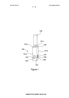
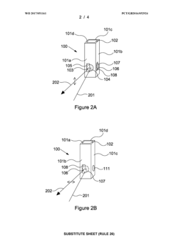
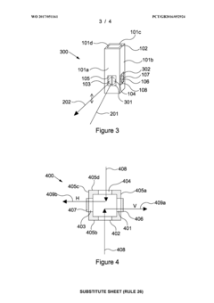
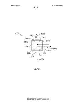
PatentWO2017051161A1
Innovation
- A cuvette carrier with integrated optical polarisers that can be retrofitted into existing DLS systems, allowing for the detection and analysis of polarised scattered light by using transmissive regions and polarisers to control and measure the polarisation of light scattered from samples, enabling DDLS measurements without the need for system upgrades.
Sample Preparation Challenges and Solutions
Sample preparation represents a critical determinant in the accuracy and reliability of nanostructure analysis when comparing Dynamic Light Scattering (DLS) and Atomic Force Microscopy (AFM) techniques. The fundamental differences in sample requirements between these methods create distinct challenges that researchers must address to obtain meaningful comparative data.
For DLS analysis, sample preparation typically involves creating a colloidal suspension with appropriate concentration. Excessive particle concentration can lead to multiple scattering effects, distorting size distribution measurements. Conversely, insufficient concentration may result in weak signal detection. The presence of dust particles or large aggregates can significantly skew results toward larger size distributions, necessitating careful filtration protocols using appropriate pore size filters (typically 0.2-0.45 μm).
Buffer composition presents another significant challenge, as ionic strength and pH directly influence the hydrodynamic diameter measured by DLS. Samples must maintain consistent buffer conditions throughout analysis to ensure reproducibility. Temperature stabilization is equally crucial, as fluctuations can alter Brownian motion dynamics and consequently affect size measurements.
AFM sample preparation involves entirely different considerations. The substrate selection becomes paramount, with mica, silicon wafers, or glass slides requiring different surface treatments to achieve optimal sample adhesion. Insufficient adhesion results in sample displacement during scanning, while excessive binding forces may distort the native nanostructure morphology.
Deposition methods significantly impact AFM imaging quality. Drop-casting often leads to uneven distribution and aggregation upon drying, while spin-coating provides more uniform coverage but may introduce shear forces that alter delicate structures. Dip-coating offers gentler deposition but with less control over surface density.
Environmental conditions during AFM imaging—particularly humidity and temperature—can dramatically affect both sample integrity and tip-sample interactions. Many biological nanostructures require imaging in liquid environments to maintain native conformations, introducing additional complexity to the experimental setup.
Cross-validation strategies have emerged to address these preparation challenges. These include sequential analysis protocols where samples are first characterized by DLS in solution, followed by controlled deposition for AFM analysis. Correlation markers and internal standards with known dimensions can help quantify preparation-induced artifacts. Advanced preparation techniques like microfluidic sample handling systems are increasingly employed to minimize contamination and ensure consistent sample transfer between analytical platforms.
Data Interpretation and Standardization Protocols
The interpretation of data from both Dynamic Light Scattering (DLS) and Atomic Force Microscopy (AFM) requires robust standardization protocols to ensure reliability and reproducibility. For DLS, the primary challenge lies in the interpretation of intensity-weighted distributions, which can be misleading when analyzing polydisperse samples. Standardized protocols typically involve multiple measurements at different concentrations and scattering angles to validate results.
A critical aspect of DLS data interpretation is the conversion from intensity-weighted to number-weighted distributions, which requires assumptions about particle shape and optical properties. Industry standards such as ISO 22412:2017 provide guidelines for this conversion process, emphasizing the importance of reporting both distributions to avoid misinterpretation.
For AFM analysis, image processing algorithms significantly impact the final results. Standardized protocols must address issues such as tip convolution effects, which can artificially enlarge lateral dimensions of nanostructures. The development of blind reconstruction algorithms has improved the accuracy of these measurements, but implementation varies across research groups.
Statistical analysis frameworks differ substantially between the two techniques. DLS provides ensemble averages from millions of particles, requiring careful consideration of weighting factors. AFM, conversely, typically samples hundreds of particles, necessitating rigorous statistical approaches to ensure representative sampling. The ASTM E2859-11 standard offers guidance on minimum sampling requirements for nanomaterial characterization.
Interlaboratory comparison studies have revealed significant variations in results when standardized protocols are not followed. The National Institute of Standards and Technology (NIST) has developed reference materials specifically for calibrating both DLS and AFM instruments, including gold nanoparticle suspensions with certified size distributions.
Data reporting formats also require standardization. The increasing adoption of FAIR (Findable, Accessible, Interoperable, and Reusable) data principles has led to the development of nanomaterial-specific data schemas. These schemas ensure that critical parameters such as sample preparation methods, instrument settings, and environmental conditions are consistently documented.
Machine learning approaches are emerging as powerful tools for data interpretation, particularly for complex nanostructures. These algorithms can identify patterns in multidimensional datasets that might be missed by conventional analysis methods. However, their implementation requires standardized training datasets to ensure reliability across different laboratory environments.
Unlock deeper insights with PatSnap Eureka Quick Research — get a full tech report to explore trends and direct your research. Try now!
Generate Your Research Report Instantly with AI Agent
Supercharge your innovation with PatSnap Eureka AI Agent Platform!