How SiC Gate Drivers Prevent Shoot-Through In Half-Bridge Power Stages?
SEP 22, 20259 MIN READ
Generate Your Research Report Instantly with AI Agent
Patsnap Eureka helps you evaluate technical feasibility & market potential.
SiC Power Electronics Background and Objectives
Silicon Carbide (SiC) power electronics has emerged as a revolutionary technology in the power semiconductor industry over the past two decades. The evolution of SiC materials began in the early 1990s, with significant breakthroughs occurring around 2010 when commercial viability was established. Unlike traditional silicon-based semiconductors, SiC offers superior properties including higher breakdown voltage, faster switching speeds, and better thermal conductivity, enabling more efficient power conversion systems.
The technological trajectory of SiC power devices has been characterized by continuous improvements in material quality, device design, and manufacturing processes. Early challenges included substrate defects, interface quality issues, and high production costs. However, recent advancements have substantially addressed these limitations, leading to wider adoption across various industries including automotive, renewable energy, and industrial applications.
Current market trends indicate an accelerating transition from silicon to SiC technology, particularly in high-voltage applications above 650V where SiC's benefits become most pronounced. This shift is driven by the global push for energy efficiency, electrification of transportation, and renewable energy integration, all of which demand more efficient power conversion solutions.
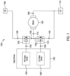
The half-bridge configuration represents one of the most fundamental building blocks in power electronics, serving as the basis for inverters, motor drives, and DC-DC converters. In SiC-based half-bridge topologies, preventing shoot-through conditions—where both high-side and low-side switches conduct simultaneously—becomes particularly critical due to the extremely fast switching speeds of SiC devices, which can reach tens of nanoseconds.
The primary technical objectives in SiC gate driver development focus on several key areas: achieving precise timing control to prevent shoot-through conditions; managing the high dv/dt and di/dt rates inherent to SiC switching; ensuring robust isolation between control and power circuits; and implementing effective protection mechanisms against overcurrent, overvoltage, and short-circuit events.
Looking forward, the technology roadmap for SiC power electronics aims to further reduce on-resistance, increase current density, improve reliability under extreme conditions, and decrease overall system costs. Specific goals include developing gate drivers capable of operating reliably at junction temperatures exceeding 200°C, reducing switching losses by optimizing gate drive parameters, and implementing advanced protection schemes with response times under 200 nanoseconds.
The convergence of wide-bandgap semiconductors like SiC with sophisticated gate driver technologies represents a pivotal advancement in power electronics, promising to enable more compact, efficient, and reliable power conversion systems across multiple industries and applications.
The technological trajectory of SiC power devices has been characterized by continuous improvements in material quality, device design, and manufacturing processes. Early challenges included substrate defects, interface quality issues, and high production costs. However, recent advancements have substantially addressed these limitations, leading to wider adoption across various industries including automotive, renewable energy, and industrial applications.
Current market trends indicate an accelerating transition from silicon to SiC technology, particularly in high-voltage applications above 650V where SiC's benefits become most pronounced. This shift is driven by the global push for energy efficiency, electrification of transportation, and renewable energy integration, all of which demand more efficient power conversion solutions.
The half-bridge configuration represents one of the most fundamental building blocks in power electronics, serving as the basis for inverters, motor drives, and DC-DC converters. In SiC-based half-bridge topologies, preventing shoot-through conditions—where both high-side and low-side switches conduct simultaneously—becomes particularly critical due to the extremely fast switching speeds of SiC devices, which can reach tens of nanoseconds.
The primary technical objectives in SiC gate driver development focus on several key areas: achieving precise timing control to prevent shoot-through conditions; managing the high dv/dt and di/dt rates inherent to SiC switching; ensuring robust isolation between control and power circuits; and implementing effective protection mechanisms against overcurrent, overvoltage, and short-circuit events.
Looking forward, the technology roadmap for SiC power electronics aims to further reduce on-resistance, increase current density, improve reliability under extreme conditions, and decrease overall system costs. Specific goals include developing gate drivers capable of operating reliably at junction temperatures exceeding 200°C, reducing switching losses by optimizing gate drive parameters, and implementing advanced protection schemes with response times under 200 nanoseconds.
The convergence of wide-bandgap semiconductors like SiC with sophisticated gate driver technologies represents a pivotal advancement in power electronics, promising to enable more compact, efficient, and reliable power conversion systems across multiple industries and applications.
Market Demand Analysis for SiC Gate Drivers
The Silicon Carbide (SiC) gate driver market is experiencing unprecedented growth driven by the rapid adoption of SiC power devices across multiple industries. Current market analysis indicates that the global SiC power semiconductor market is projected to grow at a compound annual growth rate of 29% from 2023 to 2028, with gate drivers representing a critical component within this ecosystem.
The primary market demand for SiC gate drivers stems from power electronics applications requiring high efficiency, high switching frequency, and high temperature operation. The automotive sector, particularly electric vehicles (EVs), represents the largest and fastest-growing segment. As EV manufacturers strive to extend range, reduce charging times, and decrease overall system size, SiC-based power stages with advanced gate drivers have become essential components in traction inverters, on-board chargers, and DC-DC converters.
Industrial applications constitute the second-largest market segment, with significant demand coming from solar inverters, wind power converters, and industrial motor drives. The push toward higher power density and efficiency in these applications has accelerated the transition from silicon IGBTs to SiC MOSFETs, consequently driving demand for specialized gate drivers capable of preventing shoot-through conditions in half-bridge configurations.
The telecommunications and data center sectors are emerging as substantial markets for SiC gate drivers, primarily in power supply units and uninterruptible power supplies. As data centers face increasing pressure to reduce energy consumption while handling growing computational demands, SiC-based power solutions offer compelling advantages in efficiency and power density.
Regional analysis reveals that Asia-Pacific, particularly China, Japan, and South Korea, leads in SiC gate driver adoption, followed by North America and Europe. This geographic distribution aligns with the concentration of automotive manufacturing, renewable energy development, and electronics production in these regions.
Market research indicates that customers are increasingly demanding gate drivers with integrated protection features specifically designed to prevent shoot-through conditions in half-bridge topologies. This demand is driven by the recognition that shoot-through failures can be catastrophic in high-power SiC applications, potentially resulting in system damage, downtime, and safety hazards.
The market is also showing strong preference for gate drivers offering programmable dead-time control, robust common-mode transient immunity, and advanced monitoring capabilities. These features directly address the challenges of preventing shoot-through in SiC-based power stages, where faster switching speeds and higher dv/dt rates create more demanding operating conditions compared to traditional silicon-based systems.
Technical Challenges in Half-Bridge SiC Applications
Half-bridge configurations in Silicon Carbide (SiC) power applications present several significant technical challenges that must be addressed to ensure optimal performance and reliability. The high switching speeds of SiC MOSFETs, while beneficial for efficiency, create unique difficulties in circuit design and operation.
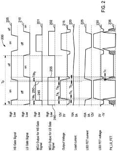
One primary challenge is the prevention of shoot-through conditions, where both high-side and low-side switches conduct simultaneously, creating a destructive short circuit across the DC bus. SiC devices switch significantly faster than traditional silicon devices, with transition times often below 10ns, drastically reducing the margin for error in timing control.
The high dv/dt rates in SiC applications, typically exceeding 50V/ns, can induce parasitic turn-on of the complementary switch through the Miller capacitance. This phenomenon becomes particularly problematic in half-bridge configurations where both switches share a common node experiencing rapid voltage transitions.
Gate drive requirements for SiC MOSFETs differ substantially from silicon counterparts. SiC devices often require higher gate voltages (+15V to +20V) for proper turn-on and negative voltages (-2V to -5V) for reliable turn-off, complicating driver design. The narrow threshold voltage margin between optimal performance and device damage necessitates precise voltage control.
Common-mode transient immunity (CMTI) represents another critical challenge. The high dv/dt rates can couple through isolation barriers in gate drivers, potentially causing false triggering. Modern SiC applications require CMTI ratings exceeding 100V/ns, pushing the limits of conventional isolation technologies.
Parasitic inductances in the power loop and gate drive loop become increasingly problematic at the high switching frequencies enabled by SiC. Even small inductances of a few nanohenries can generate substantial voltage overshoots and ringing, potentially exceeding device ratings and causing failures.
Thermal management presents unique challenges due to SiC's smaller die size compared to silicon equivalents, resulting in higher power density. The thermal resistance between junction and case must be minimized to prevent localized hotspots that can lead to device degradation or failure.
EMI generation increases substantially with faster switching, creating compliance challenges with regulatory standards. The high-frequency content of SiC switching waveforms necessitates careful PCB layout, shielding, and filtering strategies to mitigate electromagnetic interference.
These technical challenges collectively necessitate specialized gate driver solutions specifically designed for SiC applications, incorporating features like active Miller clamping, precise dead-time control, robust isolation, and temperature compensation to ensure reliable operation in half-bridge power stages.
Current Shoot-Through Prevention Methodologies
01 Dead-time control techniques for SiC gate drivers
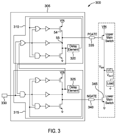
Dead-time control is a critical technique for preventing shoot-through in SiC power devices. By implementing precise timing delays between switching transitions of high-side and low-side transistors, the risk of simultaneous conduction can be minimized. Advanced dead-time control circuits can dynamically adjust these delays based on operating conditions, temperature, and load requirements, ensuring optimal performance while maintaining protection against shoot-through events.- Dead-time control techniques for SiC gate drivers: Dead-time control is a critical technique for preventing shoot-through in SiC power devices. By implementing precise timing delays between the switching of high-side and low-side transistors, the system ensures that both devices are never conducting simultaneously. Advanced dead-time control circuits can dynamically adjust these delays based on operating conditions, temperature, and load requirements, optimizing efficiency while maintaining protection against shoot-through current.
- Intelligent gate drive monitoring and protection circuits: These circuits continuously monitor gate voltage, current, and switching parameters to detect potential shoot-through conditions before they occur. When abnormal conditions are detected, protection mechanisms rapidly intervene to prevent simultaneous conduction of high-side and low-side devices. Some implementations include comparators that monitor voltage thresholds and trigger protective responses, while others employ digital logic for more sophisticated detection algorithms.
- Isolated gate driver designs for SiC applications: Electrical isolation between control circuitry and power stages is essential for preventing shoot-through in SiC applications. These designs incorporate galvanic isolation through transformers, optocouplers, or digital isolators to separate the control signals from power circuits. The isolation barrier prevents noise and transients from causing false triggering while maintaining precise timing control of gate signals, significantly reducing shoot-through risk in high-voltage SiC applications.
- Temperature-compensated gate drive solutions: SiC devices exhibit temperature-dependent switching characteristics that can increase shoot-through risk. Temperature-compensated gate drivers adjust voltage levels, slew rates, and timing parameters based on temperature feedback to maintain optimal switching performance across operating conditions. These solutions may incorporate temperature sensors, adaptive control algorithms, and variable gate resistances to ensure consistent switching behavior and prevent shoot-through regardless of junction temperature variations.
- Cross-conduction prevention through advanced timing control: Advanced timing control strategies specifically address the unique switching characteristics of SiC devices to prevent cross-conduction. These methods include asymmetric turn-on/turn-off delays, adaptive gate voltage profiles, and feedback-based timing adjustments. Some implementations use predictive algorithms to anticipate potential shoot-through conditions based on load current, bus voltage, and switching history, proactively adjusting timing parameters to maintain safe operation during high-speed switching transitions.
02 Integrated protection circuits in SiC gate drivers
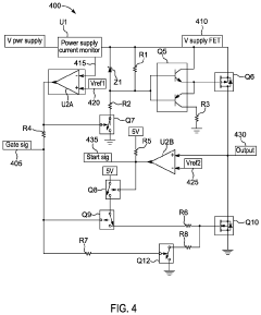
Specialized protection circuits integrated within SiC gate drivers can detect and prevent shoot-through conditions. These circuits monitor current levels, voltage transients, and switching states to identify potential shoot-through scenarios before they occur. When abnormal conditions are detected, the protection mechanisms can rapidly disable gate signals, implement soft shutdown procedures, or activate fault management systems to prevent damage to the power devices and surrounding circuitry.Expand Specific Solutions03 Advanced sensing and feedback mechanisms
Implementing sophisticated sensing and feedback mechanisms in SiC gate driver designs helps prevent shoot-through by continuously monitoring critical parameters. These systems can include current sensing, voltage monitoring, temperature feedback, and cross-conduction detection circuits. The real-time data allows for immediate response to potential shoot-through conditions, enabling the gate driver to adjust switching patterns or trigger protective measures before damage occurs.Expand Specific Solutions04 Isolation and level-shifting techniques
Proper isolation and level-shifting techniques are essential for preventing shoot-through in SiC gate drivers, particularly in high-voltage applications. These techniques ensure reliable signal transmission between control circuits and power devices while maintaining electrical isolation. Advanced isolation methods using optical, magnetic, or capacitive coupling, combined with robust level-shifting circuits, minimize the risk of spurious triggering and cross-conduction that could lead to shoot-through events.Expand Specific Solutions05 Adaptive gate drive control algorithms
Adaptive gate drive control algorithms provide intelligent management of SiC device switching to prevent shoot-through conditions. These algorithms can dynamically adjust gate voltage profiles, switching speeds, and timing parameters based on operating conditions. By implementing predictive models and real-time adjustments, these systems can optimize switching performance while maintaining robust protection against shoot-through events, even under varying load conditions, temperature fluctuations, and aging effects of the power devices.Expand Specific Solutions
Key Players in SiC Gate Driver Industry
The SiC gate driver market for half-bridge power stages is in a growth phase, with increasing adoption driven by the superior performance of SiC technology in preventing shoot-through issues. The market is expanding rapidly, projected to reach significant value as power electronics applications grow across automotive, industrial, and renewable energy sectors. Leading companies like Infineon Technologies, ROHM, Microchip Technology, and Power Integrations have achieved technical maturity with advanced isolation, propagation delay matching, and desaturation protection features. Other significant players including Mitsubishi Electric, Hitachi, and GaN Systems are developing complementary technologies, while emerging companies like VisIC Technologies and Fast SiC Semiconductor are introducing innovative solutions to address the critical challenges of preventing shoot-through in high-frequency, high-voltage applications.
Power Integrations, Inc.
Technical Solution: Power Integrations addresses shoot-through prevention in SiC half-bridge configurations through their SCALE-iDriver family. Their approach integrates Advanced Active Clamping (AAC) technology that dynamically adjusts the gate voltage during switching transients to prevent parasitic turn-on. The drivers feature FluxLink™ technology, a proprietary magnetic isolation method that provides reinforced isolation while maintaining high CMTI (Common Mode Transient Immunity) exceeding 100 V/ns. This isolation technology is crucial for preventing noise-induced false triggering during high dv/dt events. Power Integrations implements sophisticated Undervoltage Lockout (UVLO) with hysteresis on both primary and secondary sides to ensure MOSFETs remain fully off during power supply fluctuations. Their SiC-specific gate drivers include programmable dead-time control with nanosecond precision and separate source/sink outputs with adjustable drive strengths to optimize switching speed while preventing shoot-through conditions.
Strengths: Proprietary FluxLink isolation technology provides superior noise immunity; integrated protection features reduce external component count; programmable gate drive parameters allow optimization for different SiC devices. Weaknesses: Proprietary architecture may limit flexibility in some applications; higher cost compared to basic gate driver solutions; requires specific design knowledge to fully utilize advanced features.
Microchip Technology, Inc.
Technical Solution: Microchip's SiC gate driver solution employs a multi-layered approach to prevent shoot-through in half-bridge configurations. Their drivers feature Adaptive Dead Time Control (ADTC) that dynamically adjusts dead-time based on operating conditions, load current, and temperature to maintain optimal performance while preventing cross-conduction. Microchip implements advanced desaturation detection with response times under 200ns to quickly identify and mitigate potential shoot-through events. Their gate drivers incorporate Active Miller Clamp technology that provides a low-impedance path for transient currents during high dv/dt switching, effectively preventing parasitic gate turn-on. Microchip's isolation technology delivers Common Mode Transient Immunity (CMTI) ratings exceeding 100 V/ns, essential for maintaining signal integrity in high-switching-speed SiC applications. Additionally, their drivers feature independent sink/source outputs with programmable drive strengths and separate turn-on/turn-off paths, allowing precise control of switching transitions to minimize shoot-through risk.
Strengths: Adaptive dead-time control optimizes performance across operating conditions; comprehensive protection features including desaturation detection and active Miller clamping; high noise immunity with superior CMTI ratings. Weaknesses: More complex implementation requiring additional configuration; higher cost compared to basic gate driver solutions; may require more board space for complete implementation.
Core Innovations in Dead-Time Management
Gate driver circuit for high and low side switches with primary and secondary shoot-through protection
PatentInactiveUS6307409B1
Innovation
- A driver circuit with primary and secondary anti-shoot-through protection mechanisms, utilizing switch lock-out signals and gate holding paths with reduced drive capability to prevent concurrent activation of power switches and driver devices, allowing for fast switching operations while minimizing shoot-through.
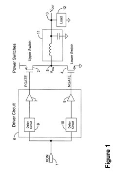
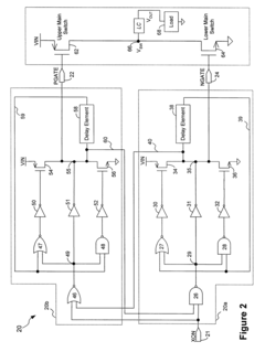
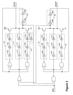
Gate driver circuit for half bridge MOSFET switches providing protection of the switch devices
PatentActiveUS11152857B2
Innovation
- A gate driver circuit that includes a signal conversion circuit to generate a high-side drive signal with a delay time that separates transitions from the low-side drive signal, and a monitoring circuit to prevent shoot-through by controlling the low-side output based on output voltage thresholds, eliminating the need for shunt resistors and dead time offsets between gate signal pairs.
Thermal Management Considerations for SiC Gate Drivers
Thermal management is a critical aspect of SiC gate driver design, particularly in half-bridge power stages where shoot-through prevention is paramount. The higher switching speeds and frequencies of SiC MOSFETs generate significant heat that must be effectively managed to maintain system reliability and performance. Without proper thermal management, gate drivers can experience degraded performance, reduced lifespan, or catastrophic failure, compromising their ability to prevent shoot-through events.
SiC gate drivers typically dissipate heat through three primary mechanisms: conduction, convection, and radiation. Conduction paths through PCB traces and thermal vias are particularly important for transferring heat away from the driver IC. Strategic placement of thermal vias beneath the driver package significantly enhances heat dissipation capabilities, with studies showing up to 30% improvement in thermal performance when properly implemented.
The power dissipation in gate drivers is predominantly influenced by switching losses, which increase proportionally with switching frequency. For SiC applications operating at frequencies above 100 kHz, gate driver power dissipation can reach 2-3W per channel, necessitating robust thermal solutions. This becomes especially critical in compact designs where multiple gate drivers are placed in close proximity.
Junction temperature management is essential for maintaining the precise timing characteristics needed for shoot-through prevention. SiC gate drivers typically have a maximum junction temperature rating of 125°C to 150°C, but operating near these limits can compromise the precise timing control required for dead-time management. Industry best practices recommend maintaining junction temperatures below 100°C to ensure optimal performance and reliability.
Thermal interface materials (TIMs) play a significant role in enhancing heat transfer between the gate driver and heat sinks or cooling structures. Advanced ceramic-filled silicone compounds with thermal conductivities exceeding 5 W/m·K are increasingly being adopted in high-performance SiC applications, offering up to 40% improvement in thermal resistance compared to conventional materials.
Environmental considerations also impact thermal management strategies. In automotive and industrial applications, ambient temperatures can vary widely, requiring adaptive thermal management approaches. Some advanced SiC gate driver solutions incorporate temperature sensors and dynamic performance adjustment capabilities to maintain optimal operation across varying thermal conditions while preserving shoot-through protection functionality.
The thermal design must also account for transient thermal events, as momentary temperature spikes during high-current switching can temporarily affect gate driver performance. Implementing sufficient thermal mass and appropriate cooling solutions helps mitigate these effects, ensuring consistent shoot-through prevention even during demanding operational scenarios.
EMI Mitigation Strategies in High-Frequency SiC Circuits
Electromagnetic Interference (EMI) presents a significant challenge in high-frequency Silicon Carbide (SiC) circuits, particularly in half-bridge power stages where shoot-through prevention is critical. The rapid switching speeds of SiC devices, while beneficial for efficiency, generate substantial electromagnetic noise that can compromise system reliability and regulatory compliance.
Traditional EMI mitigation approaches often prove inadequate for SiC-based systems due to the exceptionally fast switching transitions (dv/dt rates of 50-100 V/ns) and high operating frequencies (up to several hundred kHz). These characteristics create both conducted and radiated EMI across a broader frequency spectrum than conventional silicon-based power electronics.
Gate driver design plays a pivotal role in EMI mitigation. Advanced SiC gate drivers incorporate features such as adjustable slew rate control and precise timing management that not only prevent shoot-through conditions but also reduce EMI generation at the source. By optimizing the switching trajectory, these drivers achieve a balance between switching losses and EMI production.
Physical layout considerations become paramount in high-frequency SiC circuits. Minimizing loop areas in power and gate drive circuits reduces parasitic inductance, which otherwise contributes to voltage overshoots and ringing—major sources of EMI. Symmetrical layouts with careful consideration of current return paths significantly improve EMI performance without compromising the shoot-through protection mechanisms.
Filtering strategies must be adapted specifically for SiC applications. Multi-stage filtering approaches combining common-mode and differential-mode filters with appropriate component selection for high-frequency operation have proven effective. Specialized EMI filters with enhanced high-frequency attenuation characteristics are increasingly being developed specifically for SiC applications.
Shielding techniques require reconsideration in SiC circuits. The higher frequency components of EMI necessitate more comprehensive shielding strategies, including compartmentalization of circuit sections and strategic placement of shield materials with appropriate skin depth properties for the frequencies involved.
Grounding strategies in SiC-based systems often employ multi-point grounding techniques with careful consideration of ground plane design to minimize common-mode noise pathways. This approach must be balanced with the requirements for robust shoot-through protection, as ground potential fluctuations can trigger false switching events in sensitive gate drive circuits.
Advanced simulation tools that accurately model high-frequency behavior have become essential for predicting EMI issues before physical implementation. These tools enable designers to evaluate various mitigation strategies while ensuring that shoot-through prevention mechanisms remain effective under all operating conditions.
Unlock deeper insights with Patsnap Eureka Quick Research — get a full tech report to explore trends and direct your research. Try now!
Generate Your Research Report Instantly with AI Agent
Supercharge your innovation with Patsnap Eureka AI Agent Platform!