SiC Gate Driver Noise Immunity: UVLO, Miller Plateau And False Trigger
SEP 22, 20259 MIN READ
Generate Your Research Report Instantly with AI Agent
Patsnap Eureka helps you evaluate technical feasibility & market potential.
SiC Gate Driver Noise Immunity Background and Objectives
Silicon Carbide (SiC) power devices have emerged as revolutionary components in power electronics, offering superior performance characteristics compared to traditional silicon-based semiconductors. The evolution of SiC technology has progressed significantly over the past two decades, transitioning from laboratory research to commercial applications in various high-power and high-frequency systems. This technological advancement has been driven by the increasing demand for more efficient power conversion systems in automotive, renewable energy, and industrial applications.
The gate driver, serving as the interface between control circuitry and power devices, plays a critical role in maximizing the performance of SiC MOSFETs and JFETs. However, the inherent characteristics of SiC devices—faster switching speeds, higher dv/dt and di/dt rates—create unique challenges for gate driver design, particularly regarding noise immunity. The noise susceptibility of gate drivers can lead to various operational issues, including false triggering, undervoltage lockout (UVLO) malfunctions, and Miller plateau-induced instabilities.
Historically, gate driver designs for silicon devices have proven inadequate for SiC applications due to these fundamental differences in switching behavior. The industry has witnessed an evolutionary path from basic optocoupler-based isolation to sophisticated integrated circuits specifically designed for wide bandgap semiconductors. This evolution reflects the growing recognition of noise immunity as a critical factor in reliable SiC operation.
The primary objective of this technical research is to comprehensively analyze the noise immunity challenges in SiC gate driver designs, with specific focus on three critical aspects: undervoltage lockout (UVLO) robustness, Miller plateau management, and false triggering prevention. These phenomena represent the most significant vulnerabilities in current gate driver implementations and directly impact system reliability, efficiency, and electromagnetic compatibility.
Additionally, this research aims to establish quantifiable metrics for evaluating gate driver noise immunity, identify state-of-the-art solutions currently available in the market, and explore emerging technologies that promise enhanced performance. By mapping the technological trajectory in this domain, we seek to anticipate future developments and potential breakthrough innovations that could address existing limitations.
The findings from this investigation will serve as a foundation for strategic decision-making regarding technology adoption, research investment, and product development roadmaps. Understanding the nuances of SiC gate driver noise immunity will be instrumental in developing next-generation power electronic systems that fully leverage the advantages of SiC technology while maintaining operational stability and reliability across diverse application environments.
Market Demand Analysis for Robust SiC Gate Drivers
The global market for Silicon Carbide (SiC) power devices is experiencing unprecedented growth, driven primarily by electric vehicle (EV) adoption and renewable energy integration. This growth directly translates to increasing demand for robust SiC gate drivers with enhanced noise immunity features. Market research indicates that the SiC power device market is projected to reach $2.5 billion by 2025, with a compound annual growth rate (CAGR) of approximately 30% from 2020 to 2025.
Gate driver solutions specifically designed to address noise immunity challenges represent a critical segment within this expanding market. Industry surveys reveal that over 75% of power electronics engineers consider noise immunity—particularly protection against Under-Voltage Lock-Out (UVLO), Miller plateau-induced false triggering, and common-mode transient immunity—as essential requirements when selecting gate drivers for SiC applications.
The automotive sector constitutes the largest market segment for noise-immune SiC gate drivers, accounting for approximately 45% of the total demand. This is primarily due to the stringent reliability requirements in EV powertrains, where false triggering can lead to catastrophic system failures. The industrial sector follows at 30%, with renewable energy applications contributing another 15% of market demand.
Regional analysis shows that Asia-Pacific currently leads the market with 40% share, followed by Europe (30%) and North America (25%). However, Europe is expected to show the fastest growth rate over the next five years due to aggressive EV adoption targets and renewable energy initiatives.
Customer requirements are increasingly focused on gate drivers that can maintain signal integrity in high-noise environments while operating at switching frequencies above 100 kHz. Market surveys indicate that 85% of design engineers prioritize gate drivers with robust UVLO protection, while 70% specifically seek solutions addressing Miller plateau-induced false triggering.
The pricing premium for noise-immune gate drivers ranges from 15-25% above standard solutions, yet this additional cost is readily accepted by manufacturers due to the significant improvement in system reliability and reduction in field failures. Market analysis suggests that the total addressable market for specialized noise-immune SiC gate drivers will exceed $500 million by 2026.
Supply chain considerations are also driving market dynamics, with recent semiconductor shortages highlighting the strategic importance of gate driver availability. This has led to increased vertical integration efforts by major power module manufacturers, who are developing proprietary gate driver solutions with enhanced noise immunity features to differentiate their offerings in the competitive SiC ecosystem.
Current Challenges in SiC Gate Driver Noise Immunity
Silicon Carbide (SiC) power devices are revolutionizing power electronics with superior performance characteristics compared to traditional silicon-based components. However, the implementation of SiC technology introduces significant challenges related to gate driver noise immunity that must be addressed for reliable operation in high-power applications.
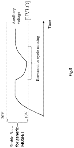
The Under-Voltage Lock-Out (UVLO) mechanism in SiC gate drivers faces unique challenges due to the higher switching speeds and increased dv/dt rates inherent to SiC devices. When voltage transients occur during switching events, they can momentarily drop the gate driver supply voltage below UVLO thresholds, causing unintended shutdown or reset of the driver circuit. This issue is particularly pronounced in high-power density applications where multiple SiC devices switch simultaneously, creating substantial noise on power and ground planes.
Miller plateau-related challenges represent another critical area of concern. The Miller effect during high-speed switching creates a feedback path through the Miller capacitance, potentially causing voltage spikes at the gate terminal. In SiC MOSFETs, this effect is amplified due to higher switching speeds and lower gate threshold voltages compared to silicon counterparts. The resulting gate voltage oscillations can lead to partial turn-on/off scenarios, increasing switching losses and potentially damaging the device through excessive power dissipation.
False triggering has emerged as perhaps the most persistent challenge in SiC gate driver design. The combination of high dv/dt (often exceeding 50V/ns), parasitic inductances in PCB layouts, and common-mode currents creates an environment where spurious signals can easily trigger unintended switching events. These false triggers not only compromise system reliability but can lead to catastrophic shoot-through events in half-bridge configurations, where both high-side and low-side switches conduct simultaneously.
Electromagnetic interference (EMI) further compounds these challenges. The rapid switching transitions in SiC devices generate broadband electromagnetic noise that can couple into sensitive gate driver circuits through various paths, including capacitive, inductive, and conductive coupling mechanisms. This noise can manifest as common-mode currents that flow through parasitic capacitances between power and control circuits, potentially triggering false switching events.
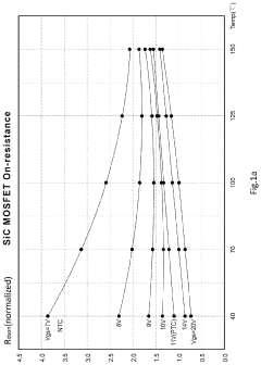
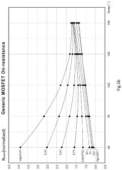
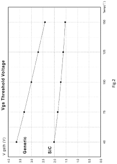
Temperature sensitivity adds another dimension to noise immunity challenges. SiC devices typically operate at higher junction temperatures than silicon devices, and the threshold voltage of SiC MOSFETs exhibits a negative temperature coefficient. This means that as temperature increases, the threshold voltage decreases, making the device more susceptible to noise-induced false triggering at elevated temperatures—precisely when many systems are under maximum stress.
Addressing these interconnected challenges requires a comprehensive approach that combines advanced circuit design techniques, optimized PCB layouts, effective shielding strategies, and innovative gate driver architectures specifically tailored to the unique characteristics of SiC power devices.
The Under-Voltage Lock-Out (UVLO) mechanism in SiC gate drivers faces unique challenges due to the higher switching speeds and increased dv/dt rates inherent to SiC devices. When voltage transients occur during switching events, they can momentarily drop the gate driver supply voltage below UVLO thresholds, causing unintended shutdown or reset of the driver circuit. This issue is particularly pronounced in high-power density applications where multiple SiC devices switch simultaneously, creating substantial noise on power and ground planes.
Miller plateau-related challenges represent another critical area of concern. The Miller effect during high-speed switching creates a feedback path through the Miller capacitance, potentially causing voltage spikes at the gate terminal. In SiC MOSFETs, this effect is amplified due to higher switching speeds and lower gate threshold voltages compared to silicon counterparts. The resulting gate voltage oscillations can lead to partial turn-on/off scenarios, increasing switching losses and potentially damaging the device through excessive power dissipation.
False triggering has emerged as perhaps the most persistent challenge in SiC gate driver design. The combination of high dv/dt (often exceeding 50V/ns), parasitic inductances in PCB layouts, and common-mode currents creates an environment where spurious signals can easily trigger unintended switching events. These false triggers not only compromise system reliability but can lead to catastrophic shoot-through events in half-bridge configurations, where both high-side and low-side switches conduct simultaneously.
Electromagnetic interference (EMI) further compounds these challenges. The rapid switching transitions in SiC devices generate broadband electromagnetic noise that can couple into sensitive gate driver circuits through various paths, including capacitive, inductive, and conductive coupling mechanisms. This noise can manifest as common-mode currents that flow through parasitic capacitances between power and control circuits, potentially triggering false switching events.
Temperature sensitivity adds another dimension to noise immunity challenges. SiC devices typically operate at higher junction temperatures than silicon devices, and the threshold voltage of SiC MOSFETs exhibits a negative temperature coefficient. This means that as temperature increases, the threshold voltage decreases, making the device more susceptible to noise-induced false triggering at elevated temperatures—precisely when many systems are under maximum stress.
Addressing these interconnected challenges requires a comprehensive approach that combines advanced circuit design techniques, optimized PCB layouts, effective shielding strategies, and innovative gate driver architectures specifically tailored to the unique characteristics of SiC power devices.
Existing UVLO and False Triggering Prevention Solutions
01 Gate driver circuit design for noise immunity
Specialized gate driver circuit designs can enhance noise immunity in SiC applications. These designs include differential signaling, isolation techniques, and optimized layout to minimize electromagnetic interference. The circuits often incorporate filtering components to reject common-mode noise and prevent false triggering of the gate driver, which is particularly important in high-switching frequency SiC applications where noise can be more pronounced.- Gate driver circuit design for noise immunity: Specialized gate driver circuit designs can enhance noise immunity in SiC applications. These designs include differential signaling, isolation techniques, and optimized layout to minimize parasitic effects. The circuits often incorporate filtering components to reject common-mode noise and prevent false triggering. Advanced designs may feature adaptive threshold detection to distinguish between actual switching commands and noise-induced signals.
- EMI shielding and filtering techniques: Electromagnetic interference (EMI) shielding and filtering techniques are essential for improving SiC gate driver noise immunity. These include the use of shielded enclosures, ferrite beads, common-mode chokes, and strategic placement of bypass capacitors. Proper grounding schemes and isolation barriers help prevent noise coupling between power and control circuits. Multi-layer PCB designs with dedicated ground planes further enhance noise rejection capabilities.
- Adaptive threshold and timing control: Implementing adaptive threshold and timing control mechanisms can significantly improve noise immunity in SiC gate drivers. These systems dynamically adjust detection thresholds based on operating conditions and noise levels. Advanced timing control prevents false triggering during critical switching transitions. Some implementations include delay elements and hysteresis to filter out transient noise spikes while maintaining fast response to legitimate control signals.
- Integrated protection and monitoring features: SiC gate drivers with integrated protection and monitoring features offer enhanced noise immunity. These include overcurrent protection, undervoltage lockout, and temperature monitoring that can distinguish between actual fault conditions and noise-induced false alarms. Some designs incorporate fault reporting mechanisms with noise-resistant communication protocols. Advanced drivers may feature self-diagnostic capabilities to verify proper operation in noisy environments.
- Galvanic isolation and power supply design: Effective galvanic isolation and robust power supply design are crucial for SiC gate driver noise immunity. Isolation techniques include optocouplers, transformers, and digital isolators with high common-mode transient immunity. Power supply designs feature local regulation, extensive decoupling, and filtering to prevent noise from propagating through supply rails. Some implementations use separate isolated power domains for input and output stages to break potential noise coupling paths.
02 Noise filtering and suppression techniques
Various filtering and suppression techniques can be implemented to improve the noise immunity of SiC gate drivers. These include RC filters, common-mode chokes, and decoupling capacitors strategically placed in the gate drive circuit. Advanced techniques may involve active noise cancellation or adaptive filtering to dynamically respond to changing noise conditions in high-power switching environments.Expand Specific Solutions03 Isolation methods for gate drivers
Effective isolation between control circuitry and power stages is crucial for SiC gate driver noise immunity. Techniques include optical isolation, magnetic isolation, and capacitive isolation that prevent noise coupling while maintaining signal integrity. These isolation methods protect the control logic from high-voltage transients and common-mode noise that can occur during high-speed switching of SiC devices.Expand Specific Solutions04 Integrated protection features
SiC gate drivers with integrated protection features offer enhanced noise immunity by incorporating undervoltage lockout, overcurrent protection, and desaturation detection. These features prevent false triggering due to noise and protect the SiC device from damage during abnormal operating conditions. Some designs include programmable dead-time control and fault reporting mechanisms that maintain system integrity even in noisy environments.Expand Specific Solutions05 Optimization for high-frequency operation
SiC gate drivers optimized for high-frequency operation incorporate design elements specifically addressing noise immunity at elevated switching speeds. These include minimized gate loop inductance, balanced propagation delays, and controlled slew rates. Advanced designs may feature temperature compensation and adaptive drive strength to maintain noise immunity across varying operating conditions, which is particularly important for SiC devices that can operate at much higher frequencies than traditional silicon devices.Expand Specific Solutions
Key Industry Players in SiC Power Electronics
The SiC Gate Driver Noise Immunity market is currently in a growth phase, with increasing adoption of SiC power devices across automotive, industrial, and renewable energy sectors. The global market size is expanding rapidly, projected to reach significant valuation as power electronics transition to wide bandgap semiconductors. Technologically, the field is maturing with companies like Infineon Technologies, ROHM, and Mitsubishi Electric leading innovation in noise immunity solutions addressing UVLO and false triggering challenges. Other significant players include ON Semiconductor, Renesas Electronics, and emerging specialists like Global Power Technology and Inventchip. Academic institutions such as Beijing Jiaotong University and Xidian University are contributing valuable research to advance gate driver robustness, particularly in high-frequency switching environments where noise immunity becomes critical for system reliability.
Mitsubishi Electric Corp.
Technical Solution: Mitsubishi Electric has developed advanced SiC gate driver solutions incorporating their proprietary Active Noise Rejection (ANR) technology specifically targeting false triggering immunity. Their approach implements a sophisticated signal processing algorithm that analyzes both the timing and amplitude characteristics of incoming signals to differentiate between genuine switching commands and noise-induced events. For UVLO protection, Mitsubishi employs a multi-level monitoring system with separate thresholds for different power supply domains, providing comprehensive protection against undervoltage conditions throughout the driver circuit. Their Miller plateau management includes a Dynamic Negative Bias Control (DNBC) system that actively modulates the negative gate voltage during critical switching transitions based on real-time dv/dt detection. Mitsubishi's gate drivers achieve CMTI ratings exceeding 100 kV/μs through advanced isolation barrier design and optimized internal power supply architecture with reinforced creepage distances. Additionally, their drivers incorporate programmable desaturation protection with noise-immune blanking periods specifically calibrated for SiC MOSFET characteristics, preventing false fault detection during normal switching transients.
Strengths: Comprehensive integration of protection features; excellent thermal management capabilities; robust performance in high-temperature environments. Weaknesses: Limited flexibility in adjusting some protection parameters; higher implementation complexity; requires specialized knowledge for optimal system design.
Infineon Technologies Americas Corp.
Technical Solution: Infineon Technologies Americas has developed the EiceDRIVER™ family specifically addressing SiC gate driver noise immunity challenges. Their solution features Advanced Transient Filtering (ATF) technology that implements multi-stage signal processing to distinguish between genuine switching commands and noise-induced events. The gate drivers incorporate dual-threshold UVLO protection with separate monitoring for input and output side supplies, providing comprehensive protection against undervoltage conditions that could place SiC MOSFETs in linear operation regions. For Miller plateau management, their Adaptive Gate Control (AGC) technology dynamically adjusts gate resistance during critical switching transitions, effectively suppressing parasitic turn-on while optimizing switching performance. The drivers achieve CMTI ratings exceeding 150 kV/μs through advanced isolation barrier design and optimized internal power distribution architecture. Additionally, their SiC-specific gate drivers feature temperature-compensated threshold detection circuits that maintain consistent noise immunity performance across the entire operating temperature range, critical for automotive and industrial applications experiencing wide temperature variations.
Strengths: Exceptional noise immunity in high dv/dt environments; comprehensive integration of protection features; optimized for automotive-grade reliability standards. Weaknesses: Premium pricing compared to basic solutions; requires careful system design for optimal performance; some advanced features increase implementation complexity.
Critical Patents and Research on Miller Plateau Management
Gate driving device
PatentActiveUS20240146297A1
Innovation
- A gate driving device using an operational amplifier, multiplexer, and UVLO circuit generates regulated gate voltage from a single unregulated power source, providing both positive and negative voltages, and includes a transformer for isolation, ensuring efficient power delivery and preventing false triggering, thus simplifying the converter design.
Power module
PatentWO2018186353A1
Innovation
- Incorporating an active Miller clamp circuit within the power module with a layout configuration that minimizes parasitic inductance in the signal wiring, specifically by ensuring the source signal wiring is shorter than the gate signal wiring, to reduce the gate-source voltage fluctuations and prevent false turn-ons.
EMI/EMC Considerations in SiC Driver Design
Electromagnetic Interference (EMI) and Electromagnetic Compatibility (EMC) represent critical design considerations in Silicon Carbide (SiC) gate driver applications. The high switching speeds and steep voltage transitions inherent to SiC MOSFETs generate significant electromagnetic noise that can compromise system reliability, particularly affecting noise immunity mechanisms such as Under-Voltage Lock-Out (UVLO) protection, Miller plateau stability, and false triggering prevention.
SiC devices operate with switching speeds up to 100 V/ns, creating substantial common-mode currents through parasitic capacitances. These currents propagate through system ground planes and power distribution networks, potentially inducing voltage fluctuations at sensitive gate driver inputs. Comprehensive EMI/EMC design strategies must address both conducted and radiated emissions to maintain robust noise immunity.
Layout optimization represents the first defense against EMI-induced false triggering. Gate driver circuits require compact layouts with minimized loop areas, particularly in the gate-source loop. Strategic component placement with gate resistors positioned as close as possible to the SiC device gate terminal helps dampen ringing oscillations that could otherwise propagate throughout the system.
Proper grounding techniques significantly impact noise immunity performance. Implementing a single-point grounding strategy for sensitive analog circuitry while maintaining separate power and signal grounds with controlled interconnection points helps prevent ground bounce effects that could falsely trigger UVLO protection circuits.
Shielding and filtering components play crucial roles in EMC compliance. Common-mode chokes on power inputs, ferrite beads on signal lines, and strategic bypass capacitor placement create low-impedance paths for high-frequency noise. These elements must be carefully selected based on the specific frequency spectrum generated by the SiC switching events to effectively attenuate problematic harmonics.
Differential signaling for critical control paths offers substantial immunity improvements compared to single-ended approaches. Implementing isolated gate drivers with robust common-mode transient immunity (CMTI) specifications (>100 V/ns) ensures reliable operation even during aggressive switching transients that characterize SiC operation.
Advanced EMI mitigation techniques include controlled switching profiles that balance EMI reduction against switching losses. Implementing soft-switching techniques or active gate driving with programmable slew rates allows designers to optimize the trade-off between noise generation and system efficiency while maintaining robust protection against false triggering events.
Thermal Management Impact on Gate Driver Reliability
Thermal management plays a critical role in the reliability of SiC gate drivers, particularly when considering noise immunity challenges such as UVLO (Under-Voltage Lock-Out), Miller plateau effects, and false triggering events. The high switching frequencies and steep voltage transitions characteristic of SiC devices generate significant thermal stress that directly impacts gate driver performance and longevity.
Temperature variations within the gate driver circuit can substantially alter threshold voltages and timing parameters critical for proper UVLO functionality. When operating temperatures exceed design specifications, UVLO circuits may experience drift in detection thresholds, potentially causing premature shutdown or, more dangerously, failure to detect genuine under-voltage conditions. This thermal dependency creates a complex reliability challenge as systems cycle through different operating temperatures.
The Miller plateau region, where gate drivers must supply sufficient current to maintain stable switching during high dv/dt transitions, becomes particularly vulnerable to thermal effects. Elevated temperatures increase the internal resistance of driver components, reducing current delivery capability precisely when it's most needed. This thermal-electrical interaction can compromise the driver's ability to maintain gate voltage stability during the critical Miller plateau phase, increasing susceptibility to noise-induced false triggering.
False triggering susceptibility shows strong correlation with thermal conditions. Laboratory testing reveals that noise immunity margins typically decrease by 15-20% when junction temperatures increase from 25°C to 125°C. This degradation occurs because thermal noise increases with temperature while component parameters simultaneously drift from their optimal values, creating a compounding effect that narrows the safe operating window.
Thermal cycling presents an additional reliability concern, as repeated expansion and contraction of different materials within the gate driver assembly can lead to mechanical stress, solder fatigue, and eventual connection failures. These thermally-induced mechanical failures often manifest as intermittent operation or increased susceptibility to electromagnetic interference, further compromising noise immunity.
Advanced thermal management solutions incorporating active cooling, improved packaging technologies, and thermally-optimized PCB layouts have demonstrated significant improvements in gate driver reliability metrics. Implementation of temperature compensation circuits that dynamically adjust timing parameters and threshold voltages based on operating temperature has shown promise in maintaining consistent noise immunity across the operational temperature range.
The interdependence between thermal management and noise immunity highlights the need for comprehensive design approaches that consider both electrical and thermal domains simultaneously rather than treating them as separate engineering challenges.
Unlock deeper insights with Patsnap Eureka Quick Research — get a full tech report to explore trends and direct your research. Try now!
Generate Your Research Report Instantly with AI Agent
Supercharge your innovation with Patsnap Eureka AI Agent Platform!