

SiC Gate Driver Power-Loop Layout: Kelvin Source, Loop Inductance And Stability
SEP 22, 20259 MIN READ
Generate Your Research Report Instantly with AI Agent
PatSnap Eureka helps you evaluate technical feasibility & market potential.
SiC Gate Driver Evolution and Objectives
Silicon Carbide (SiC) gate driver technology has undergone significant evolution over the past two decades, transforming from experimental concepts to commercially viable solutions that are revolutionizing power electronics. The journey began in the early 2000s with rudimentary gate driver designs adapted from silicon MOSFET applications, which proved inadequate for handling SiC's unique switching characteristics and higher operating voltages.
By 2010, specialized gate drivers emerged that addressed SiC's faster switching speeds and higher dv/dt requirements. These second-generation drivers incorporated improved isolation barriers and more robust protection mechanisms, yet still struggled with parasitic inductance issues inherent in traditional packaging and layout approaches.
The period from 2015 to 2020 marked a significant advancement with the introduction of integrated gate drivers specifically optimized for SiC devices. These solutions featured enhanced noise immunity, adjustable driving parameters, and began incorporating advanced monitoring capabilities. During this phase, the importance of power loop layout and Kelvin source connections gained recognition as critical factors affecting switching performance and reliability.
Current state-of-the-art gate drivers represent the fourth generation of this technology, featuring sophisticated protection schemes, ultra-low loop inductance designs, and advanced thermal management capabilities. The integration of digital control interfaces and adaptive driving parameters has further enhanced their functionality and application flexibility.
The primary objectives for SiC gate driver power-loop layout development center around several critical aspects. First, minimizing parasitic inductance in the power loop to enable faster switching transitions without voltage overshoots that could compromise device reliability. Second, optimizing Kelvin source connections to eliminate common source inductance effects that degrade switching performance and efficiency.
Additionally, ensuring switching stability across varying operating conditions remains paramount, particularly as SiC devices are deployed in increasingly demanding applications with higher power densities and operating temperatures. This requires sophisticated gate driver designs that can maintain optimal switching characteristics while preventing oscillations and EMI issues.
Future development objectives include further miniaturization of gate driver circuits while maintaining isolation integrity, integration of advanced monitoring and protection features, and development of layout techniques that can accommodate the next generation of SiC devices operating at even higher frequencies and power densities.
The ultimate goal is to create gate driver solutions that fully unlock SiC's theoretical performance advantages while ensuring long-term reliability and simplified system integration, thereby accelerating the adoption of SiC technology across automotive, renewable energy, and industrial applications.
Market Demand for High-Performance SiC Power Electronics
The global market for Silicon Carbide (SiC) power electronics is experiencing unprecedented growth, driven by increasing demands for high-efficiency power conversion systems across multiple industries. The compound annual growth rate (CAGR) for SiC power devices is projected to exceed 30% through 2026, with the market value expected to reach $2.5 billion by that time. This remarkable growth trajectory is primarily fueled by the automotive sector's rapid transition to electric vehicles (EVs), where SiC-based power modules offer significant advantages in range extension, charging speed, and overall system efficiency.
The automotive industry represents the largest market segment for SiC power electronics, accounting for approximately 60% of total demand. Major automotive manufacturers are increasingly adopting SiC technology in their EV inverters, onboard chargers, and DC-DC converters to achieve higher power density and improved thermal performance. Tesla's implementation of SiC MOSFETs in the Model 3 marked a turning point for industry-wide adoption, demonstrating tangible benefits in vehicle performance and efficiency.
Industrial applications constitute the second-largest market segment, with particular growth in renewable energy systems, industrial motor drives, and power supply units. The solar inverter market has shown particular interest in SiC technology, as higher switching frequencies enable smaller passive components and increased power density, critical factors for cost-effective renewable energy deployment.
The aerospace and defense sectors represent emerging high-value markets for SiC power electronics, where the technology's radiation hardness, high-temperature operation capability, and reliability create compelling value propositions. These sectors demand the highest performance gate driver designs with optimized power loop layouts to ensure stability under extreme operating conditions.
Market research indicates that customers across all segments are increasingly prioritizing three key performance metrics in SiC power systems: switching speed, power density, and reliability. The gate driver power-loop layout, particularly aspects like Kelvin source connections and minimized loop inductance, directly impacts all three metrics. Industry surveys show that 78% of power electronics engineers consider optimized gate driver design as "critical" or "very important" for successful SiC implementation.
Regional analysis reveals that Asia-Pacific currently leads SiC adoption, followed by North America and Europe. China's aggressive investment in electric vehicle manufacturing and renewable energy has created particularly strong demand for advanced SiC power electronics solutions with optimized gate driver designs. Government initiatives promoting energy efficiency and electrification across these regions further accelerate market growth and technology development requirements.
Current Challenges in SiC Gate Driver Power-Loop Design
Silicon Carbide (SiC) power devices have emerged as superior alternatives to traditional silicon-based semiconductors due to their higher efficiency, faster switching speeds, and better thermal performance. However, these advantages come with significant design challenges, particularly in the gate driver power-loop layout. The current challenges in SiC gate driver power-loop design center around three critical aspects: Kelvin source connections, loop inductance minimization, and overall system stability.
The Kelvin source connection represents a fundamental challenge in SiC MOSFET gate driver design. Unlike conventional source connections, Kelvin source separates the power and gate drive return paths, reducing common source inductance. However, implementing effective Kelvin source connections requires careful PCB layout considerations and component placement that many designers struggle to optimize. The physical constraints of package designs and thermal management requirements often conflict with ideal Kelvin source implementations.
Loop inductance presents another significant challenge, as SiC devices switch at much higher speeds (typically 50-100 V/ns) compared to silicon counterparts. Even small parasitic inductances in the power loop can cause substantial voltage overshoots and ringing, potentially exceeding device ratings and causing failures. Current designs struggle to achieve the ultra-low inductance levels (below 5nH) required for optimal SiC performance, particularly in higher power applications where physical distances between components increase.
Stability issues arise from the complex interaction between fast switching transients and parasitic elements. The high dv/dt and di/dt characteristics of SiC devices can trigger parasitic turn-on phenomena, common-mode currents through capacitive coupling paths, and electromagnetic interference (EMI) that disrupts control signals. These effects are particularly challenging to predict and mitigate in compact designs where thermal management demands conflict with optimal electrical layout.
Gate driver IC limitations further compound these challenges. Many commercially available gate drivers were originally designed for silicon devices and lack the performance characteristics needed for SiC applications, including insufficient common-mode transient immunity (CMTI) ratings and inadequate output current capability for the faster charging and discharging of SiC gate capacitances.
Manufacturing constraints add another layer of complexity, as the theoretical optimal layouts often prove difficult to implement in production environments. The precision required for SiC power-loop layouts pushes the boundaries of standard PCB manufacturing capabilities, leading to compromises that degrade performance or reliability.
These challenges collectively create a significant barrier to widespread SiC adoption, as designers must balance competing requirements of electrical performance, thermal management, manufacturability, and cost while developing reliable gate driver power-loop layouts.
Mainstream Power-Loop Layout Solutions
01 Minimizing loop inductance in SiC gate driver layouts
Reducing parasitic inductance in the power loop is critical for SiC gate driver stability. This can be achieved through optimized PCB layout techniques such as minimizing trace lengths, using ground planes, and implementing compact component placement. Lower loop inductance reduces voltage overshoots and ringing, improving switching performance and reducing electromagnetic interference in high-frequency SiC applications.- Minimizing loop inductance in SiC gate driver layouts: Reducing parasitic inductance in the power loop is critical for SiC gate driver stability. This can be achieved through optimized PCB layout techniques such as minimizing trace lengths, using wide copper planes, and implementing compact component placement. Lower loop inductance reduces voltage overshoots and ringing, improving switching performance and reducing EMI issues in high-frequency SiC applications.
- Gate driver circuit design for SiC stability: Specialized gate driver circuits for SiC MOSFETs incorporate features to enhance stability such as adjustable turn-on/turn-off resistors, active Miller clamp circuits, and desaturation protection. These designs help control dv/dt and di/dt rates during switching transitions, preventing parasitic turn-on and oscillations. Advanced gate driver ICs may include integrated temperature compensation and voltage regulation to maintain stable operation across varying conditions.
- Power loop layout optimization techniques: Effective power loop layout techniques for SiC gate drivers include symmetrical designs, multi-layer PCBs with dedicated power and ground planes, and strategic decoupling capacitor placement. These approaches create low-impedance current paths, minimize common-source inductance, and reduce electromagnetic coupling between control and power circuits. Advanced layouts may incorporate 3D structures and embedded components to further reduce parasitic elements.
- Thermal management for SiC gate driver stability: Thermal management is crucial for maintaining SiC gate driver stability as performance can degrade at elevated temperatures. Techniques include integrating heatsinks, thermal vias, copper pours, and active cooling systems. Proper thermal design prevents hot spots, ensures uniform temperature distribution, and extends device lifetime. Some designs incorporate temperature sensors and adaptive control algorithms to maintain stable operation across varying thermal conditions.
- EMI mitigation in SiC gate driver designs: EMI mitigation strategies for SiC gate drivers include common-mode chokes, shielding techniques, and careful signal routing to minimize interference. High dv/dt and di/dt rates in SiC devices can generate significant electromagnetic noise, requiring specialized filter networks and isolation barriers. Advanced designs may incorporate spread spectrum techniques, balanced transmission lines, and optimized grounding schemes to maintain signal integrity and system stability.
02 Gate driver circuit design for SiC stability
Specialized gate driver circuit designs can enhance the stability of SiC power devices. These include implementing active Miller clamp circuits, using separate turn-on and turn-off paths, and incorporating temperature compensation. Advanced gate driver topologies with optimized gate resistors and voltage levels help control switching speed and prevent parasitic turn-on, ensuring reliable operation under various operating conditions.Expand Specific Solutions03 Power loop layout optimization techniques
Specific layout techniques for power loops in SiC applications include symmetrical designs, multi-layer PCB structures with dedicated power and ground planes, and strategic decoupling capacitor placement. These approaches minimize current path lengths and create low-impedance connections between components. Optimized power loop layouts reduce parasitic inductance and improve thermal management, enhancing overall system stability and performance.Expand Specific Solutions04 Integrated packaging solutions for reduced inductance
Advanced packaging technologies integrate SiC devices and gate drivers in compact modules to minimize parasitic inductance. These solutions include embedded die technology, 3D packaging, and co-packaged gate drivers with power devices. Integrated designs reduce interconnection lengths and parasitic elements, enabling higher switching frequencies and improved thermal performance while maintaining stability in high-power applications.Expand Specific Solutions05 Stability enhancement through feedback and compensation
Implementing feedback mechanisms and compensation networks in SiC gate driver designs improves system stability. These include closed-loop control systems, active damping networks, and adaptive gate driving techniques that respond to operating conditions. Advanced sensing and protection features monitor voltage and current transients, adjusting gate drive parameters to maintain stable operation despite parasitic inductance effects in high-switching-speed applications.Expand Specific Solutions
Key Industry Players in SiC Power Electronics
The SiC Gate Driver Power-Loop Layout market is currently in a growth phase, characterized by increasing adoption of SiC technology in power electronics applications. The market is projected to expand significantly as electric vehicles, renewable energy systems, and industrial applications drive demand for more efficient power conversion solutions. Key players like Wolfspeed, Infineon Technologies, and ROHM are leading technological innovation, focusing on minimizing loop inductance and improving stability through advanced Kelvin source configurations. Academic institutions including Virginia Tech and Beijing Jiaotong University are collaborating with industry leaders such as Mitsubishi Electric, Toshiba, and Microchip Technology to address challenges in high-frequency switching applications. The technology is approaching maturity but continues to evolve as manufacturers seek to optimize performance, reliability, and thermal management in increasingly compact designs.
ROHM Co., Ltd.
Technical Solution: ROHM has developed a comprehensive SiC gate driver solution centered around their BM6112FV-C gate driver IC specifically designed for SiC power devices. Their approach features an innovative symmetrical layout technique that balances parasitic inductances across parallel devices, ensuring current sharing during high-speed switching. ROHM's design incorporates separate power and signal ground planes with strategic interconnection points to minimize common-mode noise coupling. Their gate drivers implement adjustable soft turn-off functionality to manage voltage overshoots during fault conditions while maintaining fast switching during normal operation. ROHM has also pioneered an active gate driving technique that dynamically adjusts gate voltage profiles during switching transitions, effectively damping oscillations without compromising switching speed. Their latest modules feature integrated temperature and current sensing with direct feedback to the gate driver, enabling real-time adjustment of switching parameters to maintain stability across operating conditions.
Strengths: Excellent integration of protection features; strong performance in high-temperature environments; comprehensive application support. Weaknesses: More limited ecosystem compared to larger competitors; some designs require specialized components; higher implementation complexity for advanced features.
Infineon Technologies AG
Technical Solution: Infineon has developed an advanced SiC gate driver solution featuring optimized Kelvin source connections that significantly reduce common source inductance. Their design incorporates a multi-layer PCB approach with dedicated power and signal layers to minimize loop inductance. Infineon's CoolSiC MOSFET gate drivers implement a split-gate resistor topology allowing independent control of turn-on and turn-off characteristics, which helps manage switching speed while maintaining stability. Their latest designs incorporate advanced EMI shielding techniques and utilize their proprietary coreless transformer technology for isolation, enabling switching frequencies above 100kHz while maintaining signal integrity. Infineon has also implemented advanced active Miller clamp circuits to prevent parasitic turn-on events caused by high dv/dt transients, which is critical for maintaining stability in high-power applications.
Strengths: Industry-leading integration of driver and protection features; comprehensive design ecosystem with simulation tools; proven reliability in automotive applications. Weaknesses: Higher cost compared to traditional silicon solutions; requires more complex thermal management; some designs may need specialized PCB manufacturing capabilities.
Critical Technologies in Kelvin Source Implementation
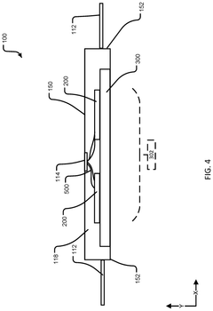
Power electronics package having signal connections for multiple power devices
PatentPendingUS20250149506A1
Innovation
- The power package includes a power substrate with SiC power devices, an assembly with specific top surface and side configurations, power contacts, signal contacts, and signal interconnections that are strategically arranged to achieve uniform gate-loop inductance and optimal signal transmission.
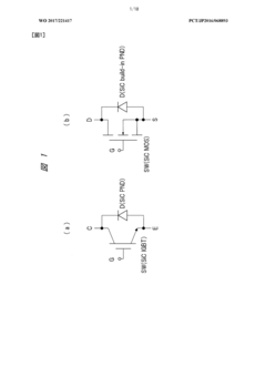
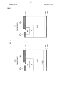
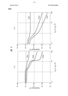
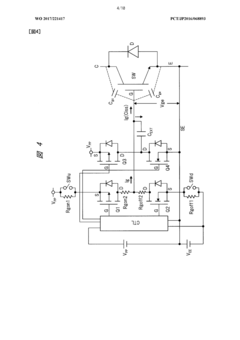
Gate drive circuit, power conversion apparatus, and railway vehicle
PatentWO2017221417A1
Innovation
- A gate drive circuit configuration that includes specific switch elements and a capacitor arrangement to control switching speed and prevent erroneous firing, utilizing PMOSFETs and NMOSFETs with built-in diode elements, and a stabilizing capacitor to manage gate drive current and capacitance, allowing for high-speed switching while reducing gate drive current.
Thermal Management Considerations for SiC Gate Drivers
Thermal management is a critical aspect of SiC gate driver design due to the high switching frequencies and power densities involved in SiC MOSFET operation. The gate driver's power loop layout significantly impacts thermal performance, as parasitic inductances and resistances can lead to increased power losses and heat generation.
When designing the thermal management system for SiC gate drivers, the Kelvin source connection plays a vital role. This connection method separates the power and signal paths, reducing common source inductance which not only improves switching performance but also decreases switching losses that contribute to heat generation. Proper implementation of Kelvin source connections can reduce thermal stress on both the gate driver and the SiC device.
Loop inductance in the gate driver power loop directly affects thermal performance. Higher inductance values lead to increased ringing and overshoot during switching transitions, resulting in additional power dissipation and localized heating. Minimizing power loop inductance through compact layout design, optimal component placement, and proper PCB layer stackup is essential for effective thermal management.
The thermal interface between the gate driver IC and its cooling solution requires careful consideration. High-performance thermal interface materials (TIMs) with low thermal resistance are recommended to efficiently transfer heat from the driver to the heatsink or cooling plate. For high-power applications, direct bonded copper (DBC) substrates or insulated metal substrates (IMS) may provide superior thermal performance compared to standard FR4 PCBs.
Temperature monitoring and protection features should be integrated into the gate driver design. Many modern gate driver ICs include built-in temperature sensors and thermal shutdown capabilities. External temperature sensing near critical components can provide additional protection and enable dynamic adjustment of switching parameters to manage thermal loads during operation.
Stability considerations in SiC gate driver design also impact thermal management. Oscillations and instability in the gate drive circuit can cause increased power dissipation and thermal stress. Proper damping resistors, optimized gate resistance values, and controlled slew rates help maintain stability while balancing switching losses and thermal performance.
Advanced cooling techniques may be necessary for high-power SiC applications. These include forced-air cooling, liquid cooling systems, or phase-change cooling solutions. The selection depends on power density, environmental conditions, and system constraints. Computational fluid dynamics (CFD) analysis can help optimize the cooling solution design and predict thermal performance under various operating conditions.
EMI Mitigation Strategies in SiC Power Circuits
Electromagnetic Interference (EMI) has become a critical concern in Silicon Carbide (SiC) power circuits due to the high switching speeds and steep voltage transitions inherent to SiC technology. The fast switching characteristics that make SiC devices advantageous for efficiency also generate significant electromagnetic noise that can compromise system reliability and regulatory compliance.
Effective EMI mitigation in SiC power circuits requires a multi-faceted approach addressing both conducted and radiated emissions. Gate driver design plays a pivotal role, where controlled switching speed through optimized gate resistance can balance EMI reduction against switching losses. Implementing soft-switching techniques further reduces EMI by minimizing dv/dt and di/dt rates during switching transitions.
Layout optimization represents one of the most effective EMI mitigation strategies. Minimizing power loop inductance through compact designs and strategic component placement significantly reduces voltage overshoots and ringing. The implementation of Kelvin source connections separates power and control current paths, preventing common-source inductance issues that exacerbate EMI generation.
Shielding and filtering constitute another critical mitigation layer. Common mode chokes, Y-capacitors, and X-capacitors effectively attenuate conducted EMI, while proper shielding techniques contain radiated emissions. The strategic placement of these components relative to noise sources maximizes their effectiveness without compromising thermal performance or power density.
Advanced modulation techniques offer algorithmic approaches to EMI reduction. Spread spectrum frequency modulation distributes switching noise across a wider frequency band, reducing peak emission levels. Random pulse width modulation introduces controlled jitter in switching patterns, similarly dispersing EMI energy across the frequency spectrum rather than concentrating it at specific frequencies.
Thermal management considerations must be integrated with EMI mitigation strategies, as thermal solutions like heatsinks can inadvertently function as EMI antennas if improperly designed. Grounding techniques are equally important, with star-point grounding and ground planes helping to minimize ground bounce and common-mode noise propagation.
Simulation and modeling tools have become essential for predicting EMI behavior before physical prototyping. Electromagnetic field simulators, circuit simulators with parasitic extraction capabilities, and specialized EMI prediction software enable designers to identify and address potential EMI issues early in the development cycle, significantly reducing design iterations and compliance testing costs.
Unlock deeper insights with PatSnap Eureka Quick Research — get a full tech report to explore trends and direct your research. Try now!
Generate Your Research Report Instantly with AI Agent
Supercharge your innovation with PatSnap Eureka AI Agent Platform!