How SiC Gate Drivers Sustain dV/dt Immunity Without Excess Gate Loss?
SEP 22, 20259 MIN READ
Generate Your Research Report Instantly with AI Agent
Patsnap Eureka helps you evaluate technical feasibility & market potential.
SiC Gate Driver Technology Background and Objectives
Silicon Carbide (SiC) power devices have emerged as revolutionary components in power electronics, offering superior performance characteristics compared to traditional silicon-based semiconductors. The evolution of SiC technology began in the early 2000s, with significant acceleration in commercial adoption occurring over the past decade. This rapid advancement has been driven by demands for higher efficiency, power density, and operational temperatures in applications ranging from electric vehicles to renewable energy systems and industrial drives.
The fundamental advantage of SiC lies in its wide bandgap properties, enabling devices to operate at higher voltages, frequencies, and temperatures than silicon counterparts. However, these same properties create unique challenges for gate driver circuits, particularly regarding dV/dt immunity without incurring excessive gate losses. The switching speeds of SiC MOSFETs and JFETs can exceed 100 V/ns, creating substantial common-mode transients that can compromise gate driver integrity.
Historical approaches to gate driver design have proven inadequate for SiC applications. Traditional optocoupler-based isolation, while effective for silicon IGBTs switching at moderate speeds, lacks the bandwidth and common-mode transient immunity (CMTI) required for SiC devices. This technological gap has spurred innovation in gate driver architectures specifically optimized for wide bandgap semiconductors.
The technical evolution trajectory shows a clear progression from basic gate drivers with minimal protection features to sophisticated integrated solutions incorporating advanced isolation technologies, precise timing control, and intelligent protection mechanisms. This evolution has been marked by the introduction of coreless transformer technology, capacitive isolation barriers, and specialized integrated circuits designed specifically for SiC switching characteristics.
The primary technical objective in SiC gate driver development is achieving the seemingly contradictory goals of maintaining robust dV/dt immunity while minimizing gate losses. This requires balancing several critical parameters: isolation barrier performance, gate loop impedance, switching speed control, and thermal management. The ideal solution must provide protection against spurious turn-on/off events while enabling efficient energy transfer to and from the gate.
Industry projections indicate that SiC power device adoption will continue accelerating, with compound annual growth rates exceeding 30% through 2028. This growth trajectory necessitates parallel advancement in gate driver technology to fully realize the potential of SiC devices across various application domains. The technical community has consequently established roadmaps targeting gate drivers capable of supporting switching speeds beyond 200 V/ns while maintaining CMTI ratings above 200 kV/μs.
The convergence of these technological trends and market demands creates both challenges and opportunities for innovation in SiC gate driver design, establishing the foundation for exploring specific technical approaches to achieving optimal performance.
Market Demand Analysis for High-Performance SiC Gate Drivers
The global market for Silicon Carbide (SiC) power devices is experiencing unprecedented growth, driven primarily by the rapid expansion of electric vehicles (EVs), renewable energy systems, and industrial automation. This growth directly translates to increasing demand for high-performance SiC gate drivers capable of maintaining dV/dt immunity without compromising efficiency through excessive gate losses.
Market research indicates that the SiC power device market is projected to grow at a CAGR of 29% through 2026, reaching approximately $2.5 billion. Gate drivers specifically designed for SiC applications represent a significant segment within this market, with automotive applications leading demand growth at over 35% annually.
The automotive sector's transition toward electrification represents the primary demand driver. Major automakers are increasingly adopting SiC-based power electronics in their EV designs to achieve higher efficiency, reduced cooling requirements, and extended range. Tesla's implementation of SiC MOSFETs in the Model 3 marked a turning point, with other manufacturers following suit. This trend has created urgent demand for gate drivers that can handle the high switching speeds of SiC while maintaining immunity to transient voltage spikes.
Industrial applications constitute the second-largest market segment, with particular growth in motor drives, uninterruptible power supplies, and industrial automation systems. These applications benefit from SiC's ability to operate at higher temperatures and frequencies, but require sophisticated gate drivers to realize these advantages safely and efficiently.
Renewable energy systems, particularly solar inverters and wind power converters, represent another rapidly expanding market segment. The push toward higher efficiency and power density in these applications aligns perfectly with SiC capabilities, creating demand for specialized gate drivers that can withstand harsh environmental conditions while maintaining optimal switching performance.
Regional analysis reveals that Asia-Pacific currently leads market demand, accounting for approximately 45% of global consumption, followed by North America (28%) and Europe (22%). China's aggressive push toward electrification and renewable energy has positioned it as the fastest-growing market for SiC gate drivers.
Customer requirements are increasingly focused on gate drivers that can maintain dV/dt immunity exceeding 100 V/ns without incurring significant gate losses. This represents a critical technical challenge that directly impacts system efficiency, reliability, and thermal management. Market surveys indicate that customers are willing to pay premium prices for gate drivers that effectively address this challenge, with over 70% of respondents identifying dV/dt immunity as a critical selection criterion.
Current Challenges in dV/dt Immunity for SiC Applications
Silicon Carbide (SiC) power devices are revolutionizing power electronics with superior switching performance and efficiency compared to traditional silicon devices. However, this advancement brings significant challenges in maintaining dV/dt immunity without compromising gate drive efficiency. The rapid voltage transitions in SiC MOSFETs and JFETs, often exceeding 50-100 V/ns, create substantial stress on gate driver circuits and surrounding components.
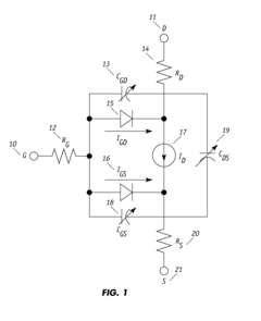
One primary challenge is the Miller effect, where high dV/dt rates during switching transitions couple through the Miller capacitance, inducing unwanted gate voltage fluctuations. These fluctuations can lead to parasitic turn-on or turn-off events, resulting in shoot-through currents and catastrophic device failures. Traditional solutions involving increased gate resistance effectively reduce dV/dt but simultaneously increase switching losses, creating an undesirable trade-off between immunity and efficiency.
Common mode transient immunity (CMTI) represents another critical challenge. The high dV/dt rates generate common mode currents through parasitic capacitances in isolation barriers, potentially corrupting gate signals or damaging sensitive control circuitry. Industry standards now demand CMTI ratings exceeding 100 V/ns for SiC applications, pushing conventional isolation technologies to their limits.
Electromagnetic interference (EMI) issues are exacerbated by high dV/dt rates, creating broadband noise that affects both the gate driver itself and surrounding control electronics. This interference can compromise signal integrity and system reliability, necessitating complex shielding and filtering solutions that add cost and complexity to the overall design.
Temperature effects further complicate dV/dt immunity challenges. SiC devices often operate at junction temperatures exceeding 175°C, altering device characteristics and potentially degrading gate oxide reliability under high dV/dt stress. Gate drivers must maintain consistent performance across this wide temperature range while protecting the device from transient overvoltage conditions.
The physical layout of gate driver circuits becomes increasingly critical with higher dV/dt rates. Parasitic inductances in gate loops can interact with fast-switching transients to create voltage overshoots and ringing, potentially exceeding device ratings. Minimizing these parasitics requires advanced packaging technologies and careful PCB layout techniques that may conflict with thermal management requirements.
Power supply requirements for gate drivers also present challenges, as isolation barriers must withstand high dV/dt while delivering clean, stable voltage to the gate driver. Conventional isolated power supplies often struggle to maintain regulation under extreme dV/dt conditions, necessitating specialized designs with higher component costs.
Current Technical Solutions for dV/dt Immunity Enhancement
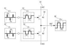
01 Gate driver circuit designs for enhanced dV/dt immunity
Various circuit designs can improve the dV/dt immunity of SiC gate drivers. These include specialized feedback loops, differential amplifier configurations, and optimized gate resistor networks that help suppress parasitic turn-on effects. Such designs can effectively filter out noise and voltage spikes that occur during high-speed switching, preventing false triggering and ensuring stable operation in high-frequency applications.- Gate driver designs for enhanced dV/dt immunity in SiC applications: Various gate driver circuit designs can improve dV/dt immunity in SiC power devices. These designs include specialized feedback loops, optimized gate resistor networks, and advanced isolation techniques that help prevent false triggering during high-speed switching events. The enhanced circuits maintain signal integrity even under extreme dV/dt conditions typical in SiC-based power converters.
- Isolation technologies for SiC gate drivers: Advanced isolation technologies are crucial for SiC gate drivers to withstand high dV/dt transients. These include galvanic isolation using transformers, optical isolation with high common-mode rejection, and capacitive isolation barriers. These technologies prevent noise coupling between the control and power sides of the circuit, ensuring reliable operation in high-voltage SiC applications.
- Common-mode noise rejection techniques: Specialized common-mode noise rejection techniques are implemented in SiC gate drivers to improve dV/dt immunity. These include differential signaling, common-mode chokes, balanced impedance networks, and active filtering. These approaches effectively suppress common-mode currents induced by rapid voltage transitions, preventing false triggering and ensuring stable operation of SiC power devices.
- Integrated protection features for SiC gate drivers: SiC gate drivers incorporate integrated protection features to enhance dV/dt immunity. These include desaturation detection, Miller clamp circuits, active Miller suppression, and undervoltage lockout. These protection mechanisms prevent parasitic turn-on during high dV/dt events, safeguarding the SiC devices from shoot-through conditions and improving overall system reliability.
- Layout and packaging considerations for dV/dt immunity: Optimized PCB layout and packaging techniques significantly impact dV/dt immunity in SiC gate driver applications. These include minimized loop areas, strategic component placement, shielding structures, and specialized grounding schemes. Proper layout reduces parasitic inductances and capacitances that can couple noise during high dV/dt events, ensuring robust operation in demanding switching environments.
02 Isolation techniques for SiC gate drivers
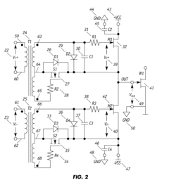
Effective isolation between control and power circuits is crucial for dV/dt immunity in SiC gate drivers. Techniques include galvanic isolation using transformers, optocouplers, or capacitive coupling methods specifically designed for high dV/dt environments. These isolation barriers prevent common-mode transients from affecting the control signals while maintaining fast response times necessary for SiC switching applications.Expand Specific Solutions03 Active Miller clamp implementations
Active Miller clamp circuits are implemented in SiC gate drivers to prevent parasitic turn-on caused by Miller capacitance during high dV/dt events. These circuits actively control the gate-source voltage during switching transitions by providing low-impedance paths to discharge the Miller current. Advanced implementations include adaptive clamp timing and variable strength clamping based on operating conditions.Expand Specific Solutions04 Power supply design for noise immunity
Robust power supply designs for gate drivers significantly improve dV/dt immunity. This includes decoupling capacitor networks, local voltage regulators with high PSRR (Power Supply Rejection Ratio), and specialized bootstrap circuits optimized for high-frequency operation. These power supply architectures maintain stable voltage levels during rapid switching transitions, preventing gate driver malfunction.Expand Specific Solutions05 Temperature compensation and protection features
SiC gate drivers with enhanced dV/dt immunity incorporate temperature compensation and protection features to maintain performance across wide operating conditions. These include adaptive gate drive strength based on temperature, thermal shutdown circuits, and specialized bias networks that adjust timing parameters to compensate for temperature-induced variations in device characteristics, ensuring reliable operation in harsh environments.Expand Specific Solutions
Key Industry Players in SiC Gate Driver Development
The SiC gate driver immunity landscape is evolving rapidly as the technology matures from early adoption to mainstream implementation. The market is projected to grow significantly, driven by electric vehicle applications and industrial power systems requiring high dV/dt immunity without compromising efficiency. Key players demonstrate varying levels of technological maturity: established semiconductor leaders like Infineon, ROHM, and ON Semiconductor offer comprehensive solutions with advanced immunity features, while emerging specialists such as Global Power Technology, Fast SiC Semiconductor, and Xinyueneng focus on innovative gate driver architectures. Academic-industry collaborations involving Xidian University, IIT Madras, and Silicon Austria Labs are accelerating development of next-generation solutions that balance immunity and gate loss optimization, indicating a competitive field with significant R&D investment across multiple regions.
Mitsubishi Electric Corp.
Technical Solution: Mitsubishi Electric has developed an advanced SiC gate driver solution that addresses dV/dt immunity challenges through their Hybrid Gate Drive Technology (HGDT). Their approach combines conventional voltage-driven and current-driven gate control methods to optimize switching behavior across different operating phases. The system features a sophisticated three-stage gate drive sequence: an initial high-current pulse for rapid channel formation, followed by a controlled slew rate phase to manage dV/dt, and finally a steady-state voltage maintenance phase with minimal power consumption[9]. Mitsubishi's gate drivers incorporate a proprietary Active Gate Clamping (AGC) circuit that provides dynamic response to transient overvoltage conditions without compromising normal switching performance. Their design includes integrated galvanic isolation with common-mode transient immunity exceeding 100 kV/μs, essential for high-frequency SiC applications. Additionally, Mitsubishi has implemented advanced thermal management techniques including temperature-compensated drive strength adjustment to maintain consistent switching characteristics across the operating temperature range. Their gate drivers also feature comprehensive fault detection and reporting capabilities, including overcurrent, overvoltage, and undervoltage protection with configurable response modes[10].
Strengths: Excellent thermal stability across wide temperature ranges; highly optimized switching trajectory control; robust isolation with superior noise immunity. Weaknesses: Higher implementation complexity requiring specialized design knowledge; premium pricing compared to basic solutions; requires careful system integration to achieve specified performance.
Infineon Technologies AG
Technical Solution: Infineon has developed advanced SiC gate driver solutions that maintain high dV/dt immunity while optimizing gate losses. Their approach incorporates a sophisticated Active Miller Clamp (AMC) technology that dynamically responds to transient conditions during switching events. This system detects unwanted gate voltage fluctuations caused by Miller capacitance and rapidly activates a low-impedance path to stabilize the gate voltage. Infineon's 1EDC-family of gate drivers implements a dual-path gate drive architecture with separate turn-on and turn-off paths, allowing independent optimization of rising and falling edge characteristics[1]. Additionally, their gate drivers feature precise undervoltage lockout (UVLO) protection and temperature-compensated current sensing to maintain consistent performance across operating conditions. The integrated galvanic isolation technology provides up to 100 kV/μs common mode transient immunity (CMTI), essential for high-frequency SiC MOSFET switching applications[2].
Strengths: Superior dV/dt immunity up to 100 kV/μs without compromising switching performance; integrated protection features reduce system complexity; scalable solution suitable for various power levels. Weaknesses: Premium pricing compared to standard gate drivers; requires careful PCB layout to maintain specified performance; higher power consumption in some protection modes.
Critical Patents and Innovations in SiC Gate Driver Design
High temperature operation silicon carbide gate driver
PatentInactiveUS20130063184A1
Innovation
- A gate driver circuit utilizing silicon on insulator (SOI) and SiC devices with high-temperature passive components, including transformers, diodes, and capacitors, operating from -70°C to 250°C and 100 kHz to 500 kHz, capable of sinking/source currents up to 25 Amperes, and providing electrical isolation and dv/dt noise minimization.
High temperature gate driver for silicon carbide metal-oxide-semiconductor field-effect transistor
PatentActiveUS11218145B2
Innovation
- A low-cost high temperature gate driver utilizing commercial-off-the-shelf discrete transistors and diodes, integrated with a robust overcurrent and under voltage lock out protection circuit, capable of operating up to 180°C, featuring a reduced propagation delay and flexible short-circuit protection, designed to minimize self-heating and enhance reliability.
Thermal Management Strategies for SiC Gate Driver Systems
Thermal management is a critical aspect of SiC gate driver design, particularly when addressing the challenge of maintaining dV/dt immunity without increasing gate losses. As SiC MOSFETs operate at higher switching frequencies and voltages than traditional silicon devices, they generate significant heat that must be effectively dissipated to ensure reliable operation and prevent thermal runaway.
The primary thermal challenges in SiC gate driver systems stem from the higher switching speeds and increased power density. When implementing robust dV/dt immunity measures, additional components such as gate resistors and common-mode chokes can become heat sources themselves, compounding the thermal management challenge. Effective thermal strategies must therefore address both the heat generated by the SiC device and the gate driver circuitry.
Heat spreading techniques represent the first line of defense in thermal management. Copper-filled vias and thick copper layers in PCB designs help distribute heat more evenly across the board surface. Strategic component placement also plays a crucial role, with temperature-sensitive components positioned away from major heat sources and power components arranged to optimize natural convection paths.
Active cooling solutions become necessary in high-power applications where passive techniques alone are insufficient. Forced-air cooling using fans or blowers can significantly enhance heat dissipation, while liquid cooling systems offer even greater thermal performance for the most demanding applications. These active solutions must be carefully integrated to avoid introducing EMI issues that could compromise the dV/dt immunity of the gate driver.
Advanced thermal interface materials (TIMs) serve as critical elements in the thermal path. Modern ceramic-filled silicone compounds, phase-change materials, and graphite sheets provide superior thermal conductivity while maintaining electrical isolation where required. The selection of appropriate TIMs can dramatically improve heat transfer from components to heatsinks or chassis structures.
Temperature monitoring and adaptive control systems represent the most sophisticated approach to thermal management. By implementing temperature sensors near critical components and utilizing feedback loops, gate driver systems can dynamically adjust operating parameters such as switching frequency or gate drive strength to maintain optimal thermal conditions while preserving dV/dt immunity performance.
Integration of these thermal management strategies must be considered early in the design process rather than as an afterthought. Thermal simulation tools enable designers to predict hotspots and optimize thermal paths before physical prototyping, significantly reducing development cycles and ensuring robust performance across the entire operating range of SiC gate driver systems.
EMI/EMC Considerations in High-Switching SiC Applications
The rapid switching capabilities of Silicon Carbide (SiC) devices, while beneficial for efficiency, introduce significant electromagnetic interference (EMI) and electromagnetic compatibility (EMC) challenges. SiC MOSFETs can switch at rates exceeding 100 V/ns, generating substantial high-frequency noise that propagates throughout power systems.
Common-mode (CM) noise presents a primary concern in SiC applications due to parasitic capacitances between switching nodes and ground. These capacitances create paths for high-frequency currents during fast dV/dt transitions, potentially disrupting nearby sensitive electronics. Differential-mode (DM) noise, occurring between power lines, further complicates EMI management in high-switching frequency environments.
Gate driver design significantly impacts EMI/EMC performance. While robust dV/dt immunity is essential, overly aggressive gate resistance values can increase switching losses. Advanced gate drivers implement sophisticated common-mode transient immunity (CMTI) features that maintain signal integrity during high dV/dt events without requiring excessive gate resistance, thus preserving switching efficiency.
Physical layout considerations become critical at high switching speeds. Minimizing loop areas in gate drive and power circuits reduces parasitic inductance that can cause voltage overshoots and ringing. Strategic component placement and careful routing of critical signals help contain EMI at its source rather than requiring extensive filtering downstream.
Shielding and filtering strategies must evolve for SiC applications. Traditional EMI filters may become less effective at the higher frequencies generated by SiC switching. Multi-stage filtering approaches incorporating both common-mode and differential-mode elements, strategically placed near noise sources, provide more effective attenuation across broader frequency spectra.
Grounding architecture requires particular attention in SiC systems. Single-point grounding strategies help prevent ground loops that can exacerbate EMI issues. Separating power and signal grounds with controlled interconnection points minimizes noise coupling between high-power switching circuits and sensitive control electronics.
Standards compliance presents additional challenges as SiC devices push operational frequencies beyond those typically addressed in traditional EMC standards. Designers must consider not only current regulatory requirements but anticipate future standards evolution as SiC adoption increases across industries. Pre-compliance testing during development becomes increasingly valuable to identify potential issues before final certification.
Unlock deeper insights with Patsnap Eureka Quick Research — get a full tech report to explore trends and direct your research. Try now!
Generate Your Research Report Instantly with AI Agent
Supercharge your innovation with Patsnap Eureka AI Agent Platform!