SiC Gate Driver CMTI: >100 kV/µs Immunity, Isolation Choices And Layout
SEP 22, 20259 MIN READ
Generate Your Research Report Instantly with AI Agent
Patsnap Eureka helps you evaluate technical feasibility & market potential.
SiC Gate Driver CMTI Evolution and Objectives
Silicon Carbide (SiC) power devices have revolutionized power electronics by enabling higher switching frequencies, greater power densities, and improved efficiency compared to traditional silicon-based semiconductors. The evolution of SiC gate driver technology has been closely tied to the advancement of SiC power devices themselves, with Common Mode Transient Immunity (CMTI) emerging as a critical parameter for reliable operation in high-voltage, high-frequency applications.
The development of SiC gate drivers began in the early 2000s with modest CMTI ratings of 15-25 kV/μs, sufficient for early SiC MOSFETs and JFETs that operated at relatively low switching speeds. As SiC device technology matured through the 2010s, switching speeds increased dramatically, necessitating gate drivers with CMTI ratings of 50-75 kV/μs to prevent false triggering and ensure reliable operation.
The current technological frontier demands CMTI ratings exceeding 100 kV/μs, driven by the latest generation of SiC power devices capable of switching at unprecedented speeds. This requirement represents a significant technical challenge that pushes the boundaries of isolation technology, circuit design, and PCB layout techniques.
The primary objective in SiC gate driver CMTI development is to achieve immunity levels above 100 kV/μs while maintaining other critical performance parameters such as propagation delay, pulse width distortion, and power consumption. This immunity must be maintained across the full operating temperature range (-40°C to 125°C) and throughout the product lifetime.
Secondary objectives include reducing the physical footprint of isolation components, improving thermal performance, and enhancing overall reliability in harsh industrial environments. Cost-effectiveness remains an important consideration as SiC technology moves from specialized applications toward mainstream adoption in automotive, renewable energy, and industrial sectors.
The technical challenges in achieving >100 kV/μs CMTI ratings stem from fundamental physics limitations in isolation barriers, parasitic capacitances in circuit designs, and electromagnetic interference effects. Addressing these challenges requires innovations in isolation technologies (magnetic, capacitive, optical), advanced semiconductor processes, and sophisticated layout techniques that minimize common-mode current paths.
Future objectives in this field include pushing CMTI ratings toward 200 kV/μs to accommodate next-generation SiC and GaN devices, while simultaneously reducing power consumption and improving integration with digital control systems. The industry is also focused on developing standardized testing methodologies for CMTI to ensure consistent performance evaluation across different manufacturers and applications.
Market Demand for High-Speed Power Electronics
The global power electronics market is experiencing unprecedented growth, driven by the rapid adoption of electric vehicles (EVs), renewable energy systems, and industrial automation. This market was valued at approximately $40 billion in 2022 and is projected to reach $73 billion by 2028, representing a compound annual growth rate (CAGR) of 10.3%. Within this expanding landscape, high-speed power electronics have emerged as a critical segment due to their ability to enhance energy efficiency, reduce system size, and improve overall performance.
Silicon Carbide (SiC) power devices are at the forefront of this technological revolution, offering superior switching speeds, higher temperature tolerance, and greater power density compared to traditional silicon-based components. The SiC power semiconductor market specifically is growing at an impressive 18.7% CAGR, outpacing the broader power electronics sector.
The demand for high-performance gate drivers with Common Mode Transient Immunity (CMTI) exceeding 100 kV/μs is being fueled by several key market factors. First, the EV market's explosive growth requires power conversion systems that can operate at higher frequencies while maintaining reliability and efficiency. Major automotive manufacturers have committed over $500 billion to electrification initiatives through 2030, creating substantial demand for advanced power electronics.
Renewable energy applications represent another significant market driver. Solar inverters and wind power converters benefit tremendously from high-speed switching capabilities, with the global solar inverter market alone expected to reach $27 billion by 2026. The ability to switch at higher frequencies directly translates to smaller passive components, reduced system costs, and improved energy harvest efficiency.
Industrial applications constitute the third major demand segment. Factory automation, motor drives, and uninterruptible power supplies increasingly require compact, efficient power conversion solutions. The industrial motor drives market, valued at $19 billion in 2022, is particularly sensitive to improvements in power density and efficiency offered by high-speed switching technologies.
Data center power infrastructure represents an emerging but rapidly growing application area. With global data center power consumption approaching 3% of worldwide electricity usage, efficiency improvements enabled by high-speed power electronics translate to significant operational cost savings and reduced environmental impact.
The market demand for these advanced gate driver solutions is further intensified by regulatory pressures worldwide. Energy efficiency standards and carbon reduction targets are becoming increasingly stringent, pushing manufacturers to adopt technologies that maximize conversion efficiency. This regulatory landscape creates a sustained demand trajectory for high-performance power electronics solutions featuring superior CMTI capabilities and robust isolation designs.
Current CMTI Challenges and Limitations
Despite significant advancements in SiC technology, achieving Common Mode Transient Immunity (CMTI) levels exceeding 100 kV/μs presents substantial challenges. Current gate driver solutions struggle with the extreme dv/dt rates inherent to SiC MOSFET switching, which can reach up to 150 kV/μs in advanced applications. This rapid voltage transition creates displacement currents through parasitic capacitances in isolation barriers, potentially causing false triggering, data corruption, or even permanent damage to gate driver circuits.
Traditional optocoupler-based isolation, while common, exhibits significant limitations at high CMTI requirements. These devices typically offer CMTI ratings of only 15-50 kV/μs, falling short of next-generation SiC requirements. Their performance degradation over temperature and lifetime further compounds reliability concerns in demanding industrial and automotive applications.
Capacitive and magnetic isolation technologies have emerged as alternatives, but each presents unique challenges. Capacitive isolators can achieve CMTI ratings of 50-100 kV/μs but remain susceptible to external electric field interference. Magnetic isolators offer improved immunity but face integration challenges and often exhibit higher power consumption, limiting their suitability for compact, efficiency-critical designs.
Layout-related limitations represent another critical challenge. Conventional PCB design practices often create unintended coupling paths that compromise CMTI performance. The parasitic capacitance between primary and secondary sides of isolation barriers frequently becomes the limiting factor in real-world implementations, with values as low as 1-2 pF significantly degrading theoretical CMTI performance.
Power supply design for gate drivers presents additional complications. The isolation barrier within power supplies must maintain integrity during high dv/dt events, requiring specialized topologies and components that add cost and complexity. Conventional designs often experience supply voltage fluctuations during transients, leading to inconsistent gate drive performance.
Testing and validation methodologies for >100 kV/μs CMTI represent a significant gap in current practices. Standard test equipment struggles to generate and accurately measure such extreme transient events, making verification challenging. This creates uncertainty in real-world performance predictions and complicates qualification processes for mission-critical applications.
Material limitations also constrain CMTI performance. Current isolation materials exhibit breakdown characteristics or parasitic behaviors that become problematic at extreme dv/dt rates. Advanced materials with superior dielectric properties and reduced parasitic effects are needed but remain in early development stages, limiting immediate implementation options.
Current >100 kV/μs CMTI Implementation Solutions
01 Gate driver design for high CMTI performance
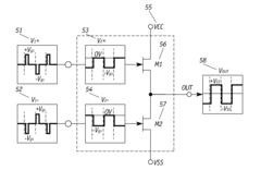
Gate driver designs specifically engineered to achieve high Common Mode Transient Immunity (CMTI) for SiC power devices. These designs incorporate specialized circuit topologies, isolation techniques, and component selection to withstand rapid voltage transitions without false triggering. High CMTI performance is critical for reliable operation of SiC-based power converters, as it prevents unwanted switching events caused by parasitic capacitive coupling during high dv/dt transients.- Gate driver design for high CMTI: Specialized gate driver designs can significantly improve Common Mode Transient Immunity (CMTI) in SiC power devices. These designs incorporate isolation barriers, optimized layout techniques, and balanced circuit configurations to withstand high dv/dt rates. Advanced gate drivers include features like Miller clamp circuits and reinforced isolation to prevent false triggering during high-speed switching events, which is particularly important for SiC devices operating at higher voltages and frequencies.
- Isolation technologies for improved CMTI: Various isolation technologies are employed to enhance CMTI performance in SiC gate drivers. These include galvanic isolation using transformers, capacitive isolation, and optical isolation methods. Advanced isolation materials and structures help maintain signal integrity while blocking common mode noise. Multi-layer isolation barriers and specialized insulation materials can significantly increase the CMTI rating, allowing gate drivers to operate reliably in high-voltage SiC applications with rapid switching transients.
- Noise suppression techniques for SiC gate drivers: Effective noise suppression techniques are critical for maintaining high CMTI in SiC gate drivers. These include common mode chokes, differential signaling, shielding, and specialized filtering circuits. Ground plane optimization and strategic component placement help minimize parasitic inductances and capacitances that can couple noise into the gate driver. Advanced noise cancellation techniques and EMI suppression methods ensure reliable operation even under extreme dv/dt conditions typical in SiC-based power converters.
- Integrated protection features for CMTI enhancement: SiC gate drivers incorporate various integrated protection features to enhance CMTI performance. These include undervoltage lockout (UVLO), desaturation detection, short-circuit protection, and active Miller clamping. Advanced gate drivers may include temperature monitoring, overcurrent protection, and soft shutdown capabilities. These protection mechanisms prevent device failure during high-stress switching events and improve overall system reliability while maintaining high CMTI ratings.
- Advanced semiconductor technologies for high CMTI gate drivers: Advanced semiconductor technologies are being developed specifically for high CMTI gate drivers used with SiC power devices. These include specialized IC processes that combine high-voltage capabilities with fast switching speeds and noise immunity. Silicon-on-insulator (SOI) technology, trench isolation, and advanced packaging techniques help improve CMTI performance. Integration of multiple functions into a single chip reduces parasitic elements and improves noise immunity, resulting in gate drivers capable of withstanding extremely high dv/dt rates.
02 Isolation technologies for SiC gate drivers
Various isolation technologies implemented in SiC gate drivers to enhance CMTI performance. These include digital isolators, transformer-based isolation, optical isolation, and capacitive isolation techniques. Advanced isolation barriers help maintain signal integrity across high potential differences while minimizing parasitic capacitance that can compromise CMTI. The isolation components are specifically designed to withstand the high dv/dt rates characteristic of SiC switching applications.Expand Specific Solutions03 Power supply design for gate drivers with high CMTI
Specialized power supply designs for gate drivers that maintain stable operation during common mode transients. These include isolated DC-DC converters with low coupling capacitance, bootstrap circuits with enhanced transient immunity, and regulated power supplies with high PSRR (Power Supply Rejection Ratio). The power supply architecture is critical for maintaining proper gate drive voltages during high-speed switching events in SiC applications.Expand Specific Solutions04 Layout and packaging techniques for CMTI improvement
PCB layout and packaging techniques that enhance CMTI performance in SiC gate driver applications. These include optimized ground plane designs, strategic component placement, shielding structures, and minimized parasitic inductances and capacitances. Advanced packaging technologies such as flip-chip, embedded die, and 3D integration help reduce parasitic elements that can degrade CMTI performance in high-frequency switching environments.Expand Specific Solutions05 Testing and measurement methods for CMTI characterization
Specialized testing and measurement methodologies for characterizing the CMTI performance of SiC gate drivers. These include standardized test procedures, custom test fixtures, and advanced measurement techniques to accurately evaluate a driver's immunity to common mode transients. The methods allow for precise quantification of CMTI parameters under various operating conditions, enabling designers to validate gate driver performance for specific SiC applications.Expand Specific Solutions
Key SiC Gate Driver Manufacturers Analysis
The SiC Gate Driver CMTI market is currently in a growth phase, driven by increasing demand for high-voltage isolation solutions exceeding 100 kV/μs in power electronics applications. The market is projected to expand significantly as electric vehicles, renewable energy systems, and industrial power conversion adopt wide bandgap semiconductors. Leading semiconductor manufacturers like Wolfspeed, ROHM, and Microchip Technology are competing with established power electronics companies including Texas Instruments, Mitsubishi Electric, and Power Integrations to develop advanced gate driver solutions. Academic institutions such as Xidian University and University of Houston are contributing research innovations, while specialized players like Delta Electronics and Littelfuse are focusing on application-specific implementations. The technology is approaching maturity in certain segments but continues to evolve with higher performance requirements and improved isolation technologies.
Wolfspeed, Inc.
Technical Solution: Wolfspeed has developed advanced SiC gate driver solutions with industry-leading CMTI performance exceeding 200 kV/μs. Their technology incorporates specialized isolation barriers using reinforced galvanic isolation with silicon dioxide (SiO2) insulation layers that maintain signal integrity during high dv/dt transients. Wolfspeed's gate drivers feature adaptive gate drive control that dynamically adjusts gate resistance based on switching conditions, optimizing the trade-off between switching speed and noise immunity. Their integrated solution includes common-mode chokes and specialized PCB layout techniques with guard rings and strategic ground plane segmentation to minimize parasitic capacitance. Wolfspeed's drivers also incorporate advanced filtering techniques to reject high-frequency noise while maintaining fast response times, and implement differential signaling for improved noise immunity in harsh electrical environments.
Strengths: Superior CMTI performance exceeding industry standards; comprehensive integration of isolation, filtering and layout optimization; specialized expertise in SiC power applications. Weaknesses: Premium pricing compared to silicon-based alternatives; requires careful system design to fully utilize performance capabilities; higher implementation complexity for engineers unfamiliar with high-performance SiC systems.
Microchip Technology, Inc.
Technical Solution: Microchip has developed the AgileSwitch® series of SiC gate drivers featuring their proprietary Augmented Switching™ technology that achieves CMTI ratings exceeding 100 kV/μs. Their solution employs digital control techniques to precisely shape switching waveforms, reducing voltage overshoot and ringing while maintaining fast switching speeds. Microchip's gate drivers utilize reinforced isolation barriers with high CTI (Comparative Tracking Index) materials and optimized creepage/clearance distances to ensure reliable operation in high-voltage applications. Their drivers incorporate programmable gate drive profiles that can be configured through a digital interface, allowing adaptive control based on operating conditions. The company's comprehensive approach includes specialized layout techniques with Kelvin source connections and optimized power/signal loop management to minimize parasitic inductances. Microchip's solutions also feature advanced protection mechanisms including short-circuit detection with response times under 1.5μs.
Strengths: Highly configurable digital control platform; excellent integration with Microchip's microcontroller ecosystem; programmable switching profiles for application optimization. Weaknesses: Digital configuration adds complexity to implementation; requires software tools for full feature utilization; higher power consumption compared to some analog alternatives.
Critical Isolation Technologies for SiC Drivers
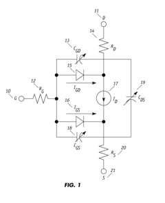
High temperature gate driver for silicon carbide metal-oxide-semiconductor field-effect transistor
PatentActiveUS11218145B2
Innovation
- A low-cost high temperature gate driver utilizing commercial-off-the-shelf discrete transistors and diodes, integrated with a robust overcurrent and under voltage lock out protection circuit, capable of operating up to 180°C, featuring a reduced propagation delay and flexible short-circuit protection, designed to minimize self-heating and enhance reliability.
High temperature operation silicon carbide gate driver
PatentInactiveUS20130063184A1
Innovation
- A gate driver circuit utilizing silicon on insulator (SOI) and SiC devices with high-temperature passive components, including transformers, diodes, and capacitors, operating from -70°C to 250°C and 100 kHz to 500 kHz, capable of sinking/source currents up to 25 Amperes, and providing electrical isolation and dv/dt noise minimization.
PCB Layout Optimization Strategies for SiC Drivers
PCB layout optimization is critical for achieving high CMTI performance in SiC gate driver applications. The layout must minimize parasitic inductances and capacitances that can compromise the driver's ability to withstand high dv/dt transients. A symmetrical layout with minimal loop areas for gate drive paths is essential, as asymmetries can lead to uneven switching and increased electromagnetic interference.
Ground plane design requires careful consideration, with separate power and signal grounds connected at a single point to prevent ground bounce issues. The isolation barrier between the high and low voltage sections must be clearly defined, with sufficient creepage and clearance distances that exceed minimum safety standards for the target voltage rating.
Component placement should prioritize the gate driver IC positioning as close as possible to the SiC device gate terminals. This minimizes gate loop inductance, which is crucial for maintaining control during high-speed switching events. Decoupling capacitors must be placed directly adjacent to power pins with minimal trace length to provide instantaneous current during switching transients.
Trace routing techniques significantly impact CMTI performance. Critical signal paths should use wider traces to reduce inductance, while sensitive signal traces should be kept short and direct. Implementing guard rings around high-voltage sections helps contain electric fields and prevents coupling to sensitive low-voltage circuits.
Multi-layer PCB designs offer superior performance for SiC applications, allowing dedicated ground planes and power planes that provide excellent shielding and low-impedance current return paths. The layer stack-up should be optimized to minimize inter-layer capacitance across the isolation barrier.
Thermal management considerations must be integrated into the layout design, as SiC devices operate at higher temperatures and switching frequencies than traditional silicon devices. Copper pours and thermal vias should be strategically placed to dissipate heat effectively from both the SiC devices and the gate driver components.
Advanced techniques such as embedded capacitance layers and controlled impedance routing can further enhance CMTI performance. These approaches help maintain signal integrity under extreme dv/dt conditions by providing more stable power delivery and reducing parasitic effects that compromise isolation performance.
Thermal Management Considerations for High-Speed Switching
High-speed switching in SiC gate drivers operating at >100 kV/μs introduces significant thermal management challenges that must be addressed to ensure reliable operation. The rapid switching transitions generate substantial heat due to switching losses, particularly during the turn-on and turn-off phases where current and voltage overlap creates power dissipation spikes.
The isolation components in gate drivers, critical for maintaining CMTI performance, are particularly susceptible to thermal stress. Optocouplers, transformers, and capacitive isolators each exhibit different thermal characteristics that affect their isolation performance under high-temperature conditions. For instance, optocouplers may experience reduced current transfer ratio (CTR) at elevated temperatures, potentially compromising isolation integrity during high dv/dt events.
Thermal gradients across isolation barriers can induce parasitic capacitances that degrade CMTI performance. These temperature-dependent effects can reduce the effective isolation capability from the specified >100 kV/μs to significantly lower values, creating potential failure points during high-speed switching operations.
Layout considerations must incorporate thermal management principles to mitigate these effects. Strategic placement of thermal vias, copper pours, and heat sinks becomes essential to direct heat away from sensitive isolation components. The physical separation between high-voltage and low-voltage domains must balance isolation requirements with thermal dissipation needs.
Advanced cooling techniques such as forced-air cooling or liquid cooling may be necessary for applications with extreme switching frequencies or high power densities. These cooling solutions must be implemented without introducing additional parasitic elements that could compromise the gate driver's CMTI performance.
Temperature monitoring and compensation circuits can be integrated to adjust gate drive parameters dynamically based on thermal conditions. This adaptive approach helps maintain optimal switching performance across varying thermal environments, preventing isolation failures during high dv/dt transients.
Material selection for PCB substrates and component packages plays a crucial role in thermal management. High thermal conductivity materials can significantly improve heat dissipation, while materials with matched thermal expansion coefficients reduce mechanical stress on isolation barriers during temperature cycling.
Simulation and thermal modeling should be employed during the design phase to identify potential hotspots and optimize thermal pathways. These models must account for the unique thermal characteristics of SiC devices, which differ substantially from traditional silicon-based semiconductors in terms of heat generation and dissipation patterns.
Unlock deeper insights with Patsnap Eureka Quick Research — get a full tech report to explore trends and direct your research. Try now!
Generate Your Research Report Instantly with AI Agent
Supercharge your innovation with Patsnap Eureka AI Agent Platform!