SiC Gate Driver Active Gate Control: dI/dt/dV/dt Shaping And Efficiency
SEP 22, 20259 MIN READ
Generate Your Research Report Instantly with AI Agent
Patsnap Eureka helps you evaluate technical feasibility & market potential.
SiC Gate Driver Evolution and Objectives
Silicon Carbide (SiC) power semiconductor technology has undergone significant evolution over the past two decades, transforming from a niche research area to a mainstream power electronics solution. The journey began in the early 2000s with rudimentary SiC diodes, followed by the introduction of first-generation SiC MOSFETs around 2010. These early devices, while promising, suffered from reliability issues, high costs, and limited gate driver compatibility.
The gate driver technology for SiC devices has evolved in parallel with the semiconductors themselves. Initial gate drivers were simple adaptations of silicon IGBT drivers, which proved inadequate for the unique switching characteristics of SiC MOSFETs. By 2015, specialized SiC gate drivers emerged, featuring higher drive voltages, faster switching capabilities, and improved noise immunity to handle the increased dv/dt and di/dt rates inherent to SiC devices.
A significant technological shift occurred around 2018 when intelligent gate drivers with basic active control features began appearing in commercial applications. These drivers incorporated rudimentary feedback mechanisms to monitor switching parameters and make limited adjustments to gate signals. This marked the beginning of the transition from passive to active gate control strategies.
The current technological frontier focuses on advanced active gate control techniques that precisely shape switching waveforms to optimize the trade-off between switching losses and electromagnetic interference (EMI). This approach represents a paradigm shift from traditional fixed gate resistance methods to dynamic control of gate current and voltage during switching transitions.
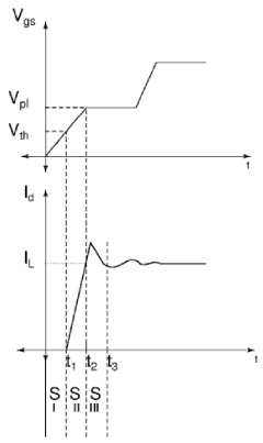
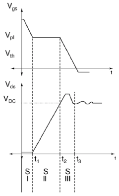
The primary objectives of modern SiC gate driver development center around three key areas: switching efficiency optimization, EMI reduction, and device protection. Active gate control aims to precisely manage dI/dt and dV/dt rates during switching transitions to minimize losses while keeping electromagnetic emissions within acceptable limits. Additionally, these advanced drivers seek to protect SiC devices from potentially damaging voltage overshoots and current spikes that can occur during high-speed switching events.
Looking forward, the industry is moving toward fully integrated gate driver solutions with embedded intelligence for real-time adaptive control. The ultimate goal is to develop gate drivers capable of dynamically adjusting switching parameters based on operating conditions, load variations, and temperature fluctuations, thereby maximizing system efficiency across all operating points while ensuring reliable operation throughout the device lifetime.
The gate driver technology for SiC devices has evolved in parallel with the semiconductors themselves. Initial gate drivers were simple adaptations of silicon IGBT drivers, which proved inadequate for the unique switching characteristics of SiC MOSFETs. By 2015, specialized SiC gate drivers emerged, featuring higher drive voltages, faster switching capabilities, and improved noise immunity to handle the increased dv/dt and di/dt rates inherent to SiC devices.
A significant technological shift occurred around 2018 when intelligent gate drivers with basic active control features began appearing in commercial applications. These drivers incorporated rudimentary feedback mechanisms to monitor switching parameters and make limited adjustments to gate signals. This marked the beginning of the transition from passive to active gate control strategies.
The current technological frontier focuses on advanced active gate control techniques that precisely shape switching waveforms to optimize the trade-off between switching losses and electromagnetic interference (EMI). This approach represents a paradigm shift from traditional fixed gate resistance methods to dynamic control of gate current and voltage during switching transitions.
The primary objectives of modern SiC gate driver development center around three key areas: switching efficiency optimization, EMI reduction, and device protection. Active gate control aims to precisely manage dI/dt and dV/dt rates during switching transitions to minimize losses while keeping electromagnetic emissions within acceptable limits. Additionally, these advanced drivers seek to protect SiC devices from potentially damaging voltage overshoots and current spikes that can occur during high-speed switching events.
Looking forward, the industry is moving toward fully integrated gate driver solutions with embedded intelligence for real-time adaptive control. The ultimate goal is to develop gate drivers capable of dynamically adjusting switching parameters based on operating conditions, load variations, and temperature fluctuations, thereby maximizing system efficiency across all operating points while ensuring reliable operation throughout the device lifetime.
Market Demand for Advanced Power Electronics
The global power electronics market is experiencing unprecedented growth, driven by the increasing demand for energy-efficient solutions across multiple industries. This market is projected to reach $25 billion by 2026, with a compound annual growth rate of 4.7%. Silicon Carbide (SiC) power devices represent one of the fastest-growing segments within this market, with adoption rates accelerating as industries seek higher performance and efficiency.
Electric vehicle (EV) manufacturers constitute the primary demand driver for advanced SiC-based power electronics. As the automotive industry transitions toward electrification, the need for high-efficiency power conversion systems has become critical. EV manufacturers require power electronics that can operate at higher voltages, temperatures, and switching frequencies while maintaining optimal efficiency to extend vehicle range and reduce charging times.
Renewable energy systems represent another significant market segment demanding advanced power electronics. Solar inverters and wind power converters benefit substantially from SiC technology's ability to operate efficiently at higher switching frequencies, reducing system size and weight while improving energy harvest rates. The global push toward renewable energy adoption has created a sustained demand trajectory for these advanced components.
Industrial applications form the third major market segment, with factory automation, motor drives, and uninterruptible power supplies increasingly adopting SiC-based solutions. These applications value the reduced cooling requirements and smaller form factors enabled by SiC's superior thermal performance and efficiency.
Data centers and telecommunications infrastructure constitute an emerging but rapidly growing market for advanced power electronics. The exponential growth in data processing demands has created critical needs for more efficient power conversion systems that can reduce energy consumption and operational costs while handling increasing power densities.
Market research indicates that customers across these segments are specifically demanding advanced gate driver solutions with active control capabilities. The ability to precisely shape switching transitions (dI/dt and dV/dt) has become a key differentiator, as it directly addresses electromagnetic interference (EMI) challenges while optimizing system efficiency.
End-users are increasingly willing to pay premium prices for power electronic solutions that can demonstrate measurable improvements in system-level efficiency, reliability, and power density. This trend is particularly evident in high-value applications such as automotive traction inverters, where the performance benefits of advanced gate control techniques translate directly to competitive advantages in the final product.
The market landscape shows regional variations, with North America and Europe leading in adoption of advanced SiC solutions for automotive and industrial applications, while Asia-Pacific demonstrates the fastest growth rate, driven by manufacturing expansion and renewable energy investments.
SiC Gate Driver Challenges and Limitations
Despite the significant advantages of Silicon Carbide (SiC) power devices, their gate driver design presents substantial challenges that limit optimal performance. The high switching speeds inherent to SiC MOSFETs create significant electromagnetic interference (EMI) issues due to rapid voltage and current transitions. These fast transitions generate common-mode currents through parasitic capacitances, resulting in conducted and radiated emissions that can disrupt nearby electronic systems.
The gate threshold voltage sensitivity of SiC devices presents another critical limitation. With narrower safe operating margins compared to silicon counterparts, SiC MOSFETs require precise gate voltage control to prevent both insufficient turn-on and gate oxide damage from overvoltage. This sensitivity necessitates tighter tolerance gate driver designs with enhanced protection mechanisms.
Parasitic inductances in the gate driver loop significantly impact SiC device performance. Even minimal inductance values can create voltage oscillations and ringing during switching transitions, potentially causing false triggering, increased switching losses, and reliability concerns. The physical layout of gate driver circuits becomes extremely critical, requiring careful consideration of trace lengths and component placement.
Temperature dependency further complicates SiC gate driver design. SiC devices exhibit varying threshold voltages and switching characteristics across their wide operating temperature range (-55°C to 200°C+). Gate drivers must compensate for these variations to maintain consistent switching performance and protection across all operating conditions.
Power supply requirements for SiC gate drivers are more demanding than silicon counterparts. They require higher gate drive voltages (typically +15V/-5V or +20V/-5V) with minimal voltage fluctuations. Additionally, the isolation components must withstand higher dV/dt rates, necessitating advanced isolation technologies with superior common-mode transient immunity.
The implementation of active gate control for dI/dt and dV/dt shaping introduces additional complexity. While essential for optimizing switching behavior and reducing EMI, these control systems require high-bandwidth sensing circuits, sophisticated control algorithms, and ultra-fast response times. The computational requirements and component precision needed for effective active gate control significantly increase system cost and complexity.
Reliability concerns also emerge from the high-frequency operation of SiC gate drivers. Components must withstand repeated high-voltage transitions and maintain performance integrity over the device lifetime. The isolation barrier degradation under high dV/dt stress represents a particular reliability challenge that requires careful component selection and design validation.
Current Active Gate Control Implementations
01 Active gate control techniques for SiC devices
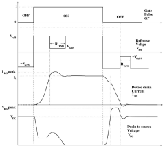
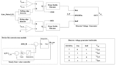
Active gate control techniques are used to optimize the switching behavior of Silicon Carbide (SiC) power devices. These techniques involve dynamically adjusting the gate drive signal to control the rate of change of current (dI/dt) and voltage (dV/dt) during switching transitions. By precisely controlling these parameters, switching losses can be reduced while maintaining electromagnetic interference (EMI) within acceptable limits, ultimately improving the overall efficiency of power conversion systems using SiC devices.- Active Gate Control Techniques for SiC MOSFETs: Active gate control techniques for Silicon Carbide (SiC) MOSFETs involve dynamic adjustment of gate drive parameters to optimize switching behavior. These techniques monitor and control the rate of change of current (dI/dt) and voltage (dV/dt) during switching transitions, reducing electromagnetic interference (EMI) and switching losses. By precisely controlling the gate voltage profile, these systems can balance between switching speed and power efficiency, extending the operational capabilities of SiC power devices.
- Gate Driver Circuit Designs for Improved Efficiency: Specialized gate driver circuit designs for SiC devices focus on improving overall system efficiency. These circuits incorporate features such as adaptive dead-time control, optimized gate resistance switching, and multi-level driving voltages to reduce switching and conduction losses. Advanced designs may include integrated temperature compensation, voltage monitoring, and protection features that maintain optimal performance across varying operating conditions while maximizing energy efficiency in power conversion applications.
- dI/dt and dV/dt Control Methodologies: Control methodologies for managing dI/dt and dV/dt in SiC gate drivers employ feedback mechanisms and predictive algorithms to shape switching waveforms. These approaches use real-time monitoring of device parameters to dynamically adjust gate drive strength, timing, and profiles. Implementation methods include closed-loop control systems, programmable gate resistance networks, and multi-stage switching sequences that can be tailored to specific application requirements, reducing stress on power devices while maintaining high switching efficiency.
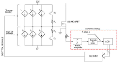
- Integrated Protection and Monitoring Features: Advanced SiC gate drivers incorporate integrated protection and monitoring features to ensure safe operation under various conditions. These systems include overcurrent detection, short-circuit protection, under-voltage lockout, and thermal monitoring capabilities. By continuously monitoring critical parameters and implementing fast response mechanisms, these gate drivers can prevent device failure during abnormal operating conditions while maintaining optimal switching performance and efficiency during normal operation.
- Resonant and Soft-Switching Techniques: Resonant and soft-switching techniques for SiC gate drivers utilize circuit topologies that enable zero-voltage switching (ZVS) or zero-current switching (ZCS) to minimize switching losses. These approaches incorporate resonant components and precisely timed switching sequences to create favorable conditions during transistor turn-on and turn-off transitions. By implementing these techniques, power converters can achieve higher operating frequencies and improved efficiency, particularly in high-power applications where traditional hard-switching would result in significant losses.
02 Gate driver circuit designs for SiC MOSFETs
Specialized gate driver circuit designs are essential for effectively driving SiC MOSFETs. These circuits typically include components such as buffer stages, isolation barriers, and protection mechanisms tailored to the unique characteristics of SiC devices. The gate driver designs incorporate features to handle the higher switching speeds, voltage levels, and temperature ranges associated with SiC technology, while providing precise control over gate voltage profiles to optimize switching performance and efficiency.Expand Specific Solutions03 dV/dt and dI/dt control methods for reducing switching losses
Various methods are employed to control the rate of change of voltage (dV/dt) and current (dI/dt) in SiC power devices to reduce switching losses. These methods include multi-level gate drive signals, variable gate resistance techniques, and feedback-based control systems that monitor switching parameters in real-time. By optimizing the switching trajectories, these control methods minimize energy dissipation during turn-on and turn-off transitions while maintaining safe operating conditions, resulting in improved thermal performance and higher overall system efficiency.Expand Specific Solutions04 Resonant and soft-switching techniques for SiC gate drivers
Resonant and soft-switching techniques are implemented in SiC gate drivers to further enhance efficiency by reducing switching losses. These approaches utilize resonant circuits, zero-voltage switching (ZVS), or zero-current switching (ZCS) methodologies to minimize the overlap between voltage and current during switching transitions. By incorporating these techniques into the gate driver design, the power dissipation associated with hard switching can be significantly reduced, enabling higher switching frequencies and improved thermal management in SiC-based power conversion systems.Expand Specific Solutions05 Integrated protection and monitoring features in SiC gate drivers
Advanced SiC gate drivers incorporate integrated protection and monitoring features to ensure reliable operation under various conditions. These features include over-current protection, short-circuit detection, under-voltage lockout, temperature monitoring, and fault reporting mechanisms. The integration of these protective functions with active gate control enables the gate driver to respond rapidly to abnormal operating conditions while maintaining optimal switching performance during normal operation, thereby enhancing the robustness and longevity of SiC-based power systems.Expand Specific Solutions
Key Industry Players in SiC Power Electronics
The SiC Gate Driver Active Gate Control market is currently in a growth phase, driven by increasing demand for efficient power electronics in automotive, industrial, and renewable energy sectors. The market size is expanding rapidly, projected to reach significant value as Silicon Carbide (SiC) adoption accelerates across high-power applications. Technologically, the field is maturing with companies like Infineon Technologies, ROHM, and Microchip Technology leading innovation in dI/dt and dV/dt shaping techniques. Established players including Mitsubishi Electric, ABB Group, and Renesas Electronics are advancing commercial implementations, while automotive manufacturers such as Toyota and Tesla are driving application-specific developments. Research institutions like Silicon Austria Labs and University of Electronic Science & Technology of China are contributing to fundamental breakthroughs in efficiency optimization and switching performance.
Mitsubishi Electric Corp.
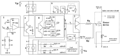
Technical Solution: Mitsubishi Electric has developed an advanced Active Gate Control technology for SiC power devices that focuses on balancing switching performance with system reliability. Their approach utilizes a multi-level gate voltage control scheme that provides precise management of both turn-on and turn-off transients. The technology incorporates real-time monitoring of device parameters and implements feedback control loops that continuously adjust gate drive characteristics to maintain optimal switching behavior. Mitsubishi's solution features proprietary algorithms that analyze switching waveforms and apply corrective measures to minimize oscillations and overshoot while maximizing efficiency. Their gate drivers implement variable slew rate control that can be dynamically adjusted based on load conditions and temperature variations[6]. The system includes programmable delay elements that enable fine-tuning of switching sequences in multi-device configurations, reducing system-level EMI and improving overall performance. Mitsubishi's implementation also features comprehensive protection mechanisms that respond to abnormal operating conditions while maintaining high efficiency during normal operation.
Strengths: Excellent balance between switching speed and EMI performance, particularly suitable for high-power applications. Comprehensive protection features enhance system reliability without significant efficiency penalties. Weaknesses: Relatively complex implementation requiring careful system design. May require more board space compared to simpler solutions due to additional control circuitry.
ABB Group
Technical Solution: ABB has developed a sophisticated Active Gate Control technology for SiC devices that focuses on system-level optimization and industrial reliability. Their approach implements a hybrid analog-digital control architecture that provides both rapid response and complex decision-making capabilities. ABB's gate drivers feature multi-point voltage sensing and current monitoring that enable precise control of switching trajectories under varying load conditions. The technology incorporates predictive algorithms that anticipate switching behavior based on historical data and operating parameters, allowing for proactive adjustments to gate drive signals. ABB's solution includes adaptive impedance matching networks that optimize power transfer between the driver and gate, reducing losses and improving switching efficiency[5]. Their implementation features configurable dV/dt and dI/dt limits that can be adjusted based on EMI requirements and system constraints. The technology also includes advanced thermal management techniques that maintain optimal switching characteristics even under extreme temperature conditions, making it particularly suitable for demanding industrial applications.
Strengths: Robust design with excellent reliability in harsh industrial environments. Advanced thermal management ensures consistent performance across wide temperature ranges. Weaknesses: Higher initial cost compared to simpler gate drive solutions. System complexity may require specialized expertise for implementation and maintenance.
Core Technologies for dI/dt and dV/dt Shaping
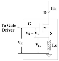
Digitally controlled switched current source active gate driver for silicon carbide mosfet with line current sensing
PatentActiveIN201741020104A
Innovation
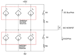
- A digitally controlled switched current source active gate driver with a novel current sensing technique using a kelvin inductor is implemented, featuring a four-step control method and a low-frequency control loop to precisely manage the rate of rise and fall of device current and voltage, and a low-speed control loop to adjust switching steps based on previous cycles.
Closed loop active gate driver unit using high band width controlled current source with dynamic gate voltage clamping
PatentActiveIN201641042631A
Innovation
- A novel analog current controller-based closed-loop active gate driver that dynamically applies higher gate voltages and controls di/dt and dv/dt values to reduce switching losses and suppress voltage spikes, using a proportional closed-loop gate current controller and RC differentiator circuit to inject high-bandwidth current signals into the SiC MOSFET.
Thermal Management Considerations
Thermal management represents a critical consideration in SiC gate driver design implementing active gate control techniques. The high switching frequencies and power densities characteristic of SiC MOSFETs generate significant thermal loads that must be effectively managed to ensure reliable operation and maximize device lifetime.
The thermal challenges in active gate control systems stem from multiple sources. Gate drivers themselves dissipate power during switching transitions, particularly when implementing sophisticated dI/dt and dV/dt control algorithms that may require multiple switching stages or variable resistance paths. This power dissipation increases proportionally with switching frequency, creating localized hot spots within the gate driver circuitry.
SiC MOSFETs exhibit thermal characteristics distinct from traditional silicon devices, including higher thermal conductivity but also greater sensitivity to temperature variations that can affect switching performance. The relationship between junction temperature and switching losses becomes particularly important when implementing active gate control, as temperature fluctuations can alter the effectiveness of carefully calibrated dI/dt and dV/dt profiles.
Advanced thermal management solutions for SiC gate driver systems typically incorporate multi-layered approaches. Heat spreading techniques using specialized PCB designs with increased copper thickness and thermal vias help distribute heat away from critical components. Dedicated thermal interface materials (TIMs) with optimized thermal conductivity facilitate efficient heat transfer to cooling structures.
Active cooling solutions ranging from forced air to liquid cooling systems may be necessary for high-power applications where passive cooling proves insufficient. The selection of appropriate cooling methodology must balance thermal performance against system complexity, reliability, and cost considerations.
Thermal modeling and simulation play essential roles in the design process, enabling accurate prediction of temperature distributions and identification of potential thermal bottlenecks. Advanced computational fluid dynamics (CFD) simulations can optimize heat sink designs and airflow patterns to maximize cooling efficiency.
Temperature monitoring and adaptive control mechanisms represent emerging approaches to thermal management in advanced gate driver systems. By incorporating temperature feedback into gate control algorithms, the system can dynamically adjust switching parameters to maintain optimal performance while preventing thermal runaway conditions. This adaptive approach ensures maximum efficiency across varying operating conditions while maintaining safe thermal margins.
EMI Mitigation Strategies
Electromagnetic Interference (EMI) mitigation represents a critical aspect of SiC power converter design due to the high switching speeds inherent in SiC technology. Active gate control techniques offer significant advantages in managing EMI emissions through precise control of switching transients.
The fundamental approach to EMI mitigation through active gate control involves strategically shaping the dV/dt and dI/dt profiles during switching transitions. By implementing variable gate resistance or multi-level gate voltage profiles, designers can effectively reduce high-frequency noise components while maintaining acceptable switching losses. These techniques create smoother switching transitions that significantly reduce electromagnetic emissions across both conducted and radiated spectra.
Advanced closed-loop control systems represent the state-of-the-art in EMI mitigation strategies. These systems continuously monitor switching parameters and dynamically adjust gate drive signals in real-time, responding to changing operating conditions. Implementation typically involves high-speed analog feedback circuits or digital signal processors capable of nanosecond-level response times, enabling precise control over switching trajectories.
Frequency-domain optimization techniques have emerged as particularly effective for targeted EMI reduction. By analyzing the spectral content of switching waveforms, gate drive profiles can be specifically tailored to minimize energy at problematic frequencies. This approach allows designers to focus mitigation efforts on frequency bands most relevant to their application's EMC requirements, optimizing the trade-off between EMI performance and switching efficiency.
Layout considerations play a crucial complementary role to active gate control in comprehensive EMI management. Minimizing gate loop inductance, implementing Kelvin source connections, and strategic placement of decoupling capacitors significantly enhance the effectiveness of active gate control techniques. The synergistic combination of optimized layout and active gate control can achieve EMI reductions of 15-20 dB across critical frequency bands compared to conventional gate driving methods.
Recent research demonstrates that predictive control algorithms can anticipate EMI generation patterns based on operating conditions and preemptively adjust gate drive parameters. These algorithms leverage machine learning techniques to develop models that correlate switching conditions with EMI signatures, enabling more sophisticated mitigation strategies that adapt to complex operating environments.
Unlock deeper insights with Patsnap Eureka Quick Research — get a full tech report to explore trends and direct your research. Try now!
Generate Your Research Report Instantly with AI Agent
Supercharge your innovation with Patsnap Eureka AI Agent Platform!