How To Design Photocell Circuits For Low Power Consumption
AUG 21, 202510 MIN READ
Generate Your Research Report Instantly with AI Agent
Patsnap Eureka helps you evaluate technical feasibility & market potential.
Photocell Circuit Evolution and Objectives
Photocell circuits have undergone significant evolution since their inception, driven by the increasing demand for energy-efficient solutions in various applications. The journey of these circuits began with simple designs that primarily focused on functionality rather than power consumption. As technology advanced and energy conservation became a priority, the objectives for photocell circuit design shifted towards achieving optimal performance while minimizing power usage.
In the early stages, photocell circuits were predominantly used in basic light-sensing applications, such as automatic street lighting and daylight harvesting systems. These initial designs often relied on continuous power consumption, even when not actively sensing light changes. The primary goal was to ensure reliable light detection and switching capabilities, with little emphasis on energy efficiency.
As the electronics industry progressed, the focus gradually shifted towards developing more sophisticated and energy-conscious photocell circuits. This evolution was driven by several factors, including the growing awareness of environmental issues, the need for longer battery life in portable devices, and the increasing adoption of photocell technology in a wider range of applications.
The objectives for modern photocell circuit design have become multifaceted, with low power consumption taking center stage. Engineers now strive to create circuits that can operate effectively while drawing minimal current, especially during idle periods. This has led to the development of innovative circuit topologies and the integration of advanced power management techniques.
One of the key objectives in contemporary photocell circuit design is to implement intelligent power-saving modes. These modes allow the circuit to enter a low-power state when light conditions remain stable, significantly reducing overall energy consumption. Additionally, designers aim to optimize the circuit's response time, ensuring rapid wake-up from power-saving modes when light conditions change, without compromising on accuracy or reliability.
Another important goal is to enhance the circuit's sensitivity and dynamic range while maintaining low power requirements. This involves careful selection of components, such as high-efficiency photodetectors and low-power operational amplifiers, as well as implementing advanced signal processing techniques to extract meaningful data from weak light signals.
The integration of photocell circuits with microcontrollers and other digital systems has also become a key objective. This integration allows for more sophisticated control algorithms, adaptive power management, and the ability to communicate with other systems, further expanding the potential applications of photocell technology while keeping power consumption in check.
As we look towards the future, the objectives for photocell circuit design continue to evolve. Emerging goals include the development of self-powered photocell circuits that can harvest energy from ambient light, as well as the integration of machine learning algorithms to predict lighting patterns and optimize power usage accordingly. These advancements promise to push the boundaries of energy efficiency in photocell applications even further.
Low Power IoT Market Analysis
The low power IoT market has been experiencing significant growth in recent years, driven by the increasing demand for energy-efficient and long-lasting connected devices. This market segment is particularly relevant to photocell circuit design for low power consumption, as these circuits are often integral components in IoT devices that require minimal energy usage.
The global low power IoT market is expected to continue its upward trajectory, with projections indicating substantial expansion over the next five years. This growth is fueled by the proliferation of smart home devices, industrial IoT applications, and the increasing adoption of wireless sensor networks across various sectors.
One of the key drivers of this market is the growing emphasis on sustainability and energy conservation. As businesses and consumers become more environmentally conscious, there is a rising demand for IoT devices that can operate for extended periods on limited power sources, such as batteries or energy harvesting systems. This trend directly aligns with the need for efficient photocell circuit designs that minimize power consumption.
The industrial sector represents a significant portion of the low power IoT market, with applications in predictive maintenance, asset tracking, and environmental monitoring. These use cases often require sensors and devices to operate in remote or hard-to-reach locations, making low power consumption a critical factor. Photocell circuits that can operate efficiently in these conditions are highly sought after in this segment.
In the consumer market, smart home devices and wearables are driving demand for low power IoT solutions. These products often incorporate light sensors for various functions, such as automatic brightness adjustment or ambient light detection. The ability to design photocell circuits that consume minimal power is crucial for extending battery life and improving overall user experience in these devices.
The healthcare sector is another area where low power IoT devices are gaining traction. Remote patient monitoring systems and medical wearables rely on long-lasting, energy-efficient sensors, including those based on photocell technology. The market for these applications is expected to grow rapidly, creating opportunities for innovative low power circuit designs.
Geographically, North America and Europe currently lead the low power IoT market, with Asia-Pacific showing the fastest growth rate. This regional distribution is influenced by factors such as technological infrastructure, regulatory environments, and industrial development. The demand for efficient photocell circuits is likely to follow similar patterns, with variations based on specific application needs in different regions.
As the low power IoT market continues to evolve, there is an increasing focus on developing more efficient power management techniques and energy harvesting solutions. This trend presents both challenges and opportunities for photocell circuit designers, who must balance performance requirements with stringent power consumption constraints to meet market demands.
Current Challenges in Photocell Power Efficiency
Photocell circuits face several significant challenges in achieving low power consumption, which is crucial for energy-efficient applications and extended battery life in portable devices. One of the primary obstacles is the inherent power consumption of the photocell itself, even in low-light conditions. Traditional photocells often exhibit a continuous current draw, leading to unnecessary power drain when not actively sensing light.
Another major challenge lies in the design of the supporting circuitry. Amplifiers and comparators, commonly used in photocell circuits, can contribute substantially to overall power consumption. These components often require a constant supply current, which can quickly deplete battery resources in long-term deployments. Balancing sensitivity and power efficiency in these supporting components remains a complex task for circuit designers.
The issue of dark current presents a significant hurdle in low-power photocell circuit design. Dark current, the small electric current that flows through photosensitive devices even when no photons are entering the device, can lead to false readings and unnecessary power consumption. Minimizing dark current without compromising the photocell's sensitivity is a delicate balance that engineers must strike.
Temperature sensitivity is another critical challenge. Photocells and their associated circuitry can exhibit varying behavior across different temperature ranges, potentially leading to increased power consumption or reduced accuracy in extreme conditions. Designing circuits that maintain consistent performance and low power consumption across a wide temperature range adds complexity to the development process.
The need for continuous monitoring in many applications poses a significant power efficiency challenge. Constantly powering the photocell and its associated circuitry can quickly drain power sources. Implementing effective power management strategies, such as duty cycling or adaptive sampling rates, without compromising the circuit's responsiveness to light changes is a complex task that requires careful consideration.
Noise reduction in low-power photocell circuits presents another hurdle. As power consumption is reduced, the signal-to-noise ratio often decreases, making it more challenging to accurately detect and measure light levels. Implementing effective noise reduction techniques while maintaining low power consumption adds another layer of complexity to circuit design.
Lastly, the challenge of integrating photocell circuits with other low-power systems and microcontrollers introduces additional power management considerations. Ensuring seamless communication and synchronization between the photocell circuit and other system components, while minimizing overall power consumption, requires sophisticated design approaches and often involves trade-offs between functionality and energy efficiency.
Existing Low Power Photocell Circuit Designs
01 Power management in photocell circuits
Efficient power management techniques are implemented in photocell circuits to reduce overall power consumption. These methods include optimizing circuit design, implementing power-saving modes, and utilizing advanced control algorithms to regulate power usage based on ambient light conditions.- Power-saving techniques in photocell circuits: Various methods are employed to reduce power consumption in photocell circuits. These include implementing sleep modes, using low-power components, and optimizing circuit design to minimize energy usage during inactive periods. Such techniques help extend battery life in portable devices and improve overall energy efficiency.
- Adaptive power management in photocell systems: Adaptive power management systems are designed to dynamically adjust power consumption based on environmental conditions and usage patterns. These systems may incorporate sensors and microcontrollers to monitor light levels and adjust circuit operation accordingly, maximizing energy efficiency while maintaining optimal performance.
- Integration of photocells with energy-efficient lighting systems: Photocells are integrated into energy-efficient lighting systems to automatically control illumination based on ambient light levels. This integration helps reduce unnecessary power consumption by ensuring lights are only activated when needed, contributing to overall energy savings in various applications such as street lighting and building automation.
- Low-power photocell circuit design for IoT applications: Specialized low-power photocell circuit designs are developed for Internet of Things (IoT) applications. These circuits often incorporate ultra-low-power microcontrollers, energy harvesting techniques, and optimized sensor interfaces to minimize power consumption while maintaining connectivity and functionality in distributed sensor networks.
- Power-efficient signal processing in photocell-based systems: Advanced signal processing techniques are employed to enhance the efficiency of photocell-based systems. These may include implementing digital signal processing algorithms, using adaptive filtering, and optimizing analog-to-digital conversion processes to reduce computational load and power consumption while maintaining high accuracy in light detection and measurement.
02 Low-power photocell circuit designs
Innovative circuit designs are developed to minimize power consumption in photocell applications. These designs incorporate energy-efficient components, reduce standby power, and optimize signal processing to achieve lower overall power requirements while maintaining performance.Expand Specific Solutions03 Energy harvesting in photocell systems
Photocell circuits are integrated with energy harvesting technologies to reduce reliance on external power sources. These systems capture and store energy from ambient light or other environmental sources, effectively lowering the overall power consumption of the device.Expand Specific Solutions04 Adaptive power control for photocell circuits
Adaptive power control mechanisms are implemented in photocell circuits to dynamically adjust power consumption based on environmental conditions and system requirements. These systems use intelligent algorithms to optimize power usage while maintaining desired functionality.Expand Specific Solutions05 Integration of photocell circuits with low-power microcontrollers
Photocell circuits are integrated with low-power microcontrollers to achieve improved energy efficiency. These integrated systems leverage the power-saving features of modern microcontrollers to reduce overall power consumption while enhancing functionality and control capabilities.Expand Specific Solutions
Key Players in Low Power Photocell Industry
The photocell circuit design for low power consumption market is in a mature stage, with established players and ongoing innovation. The market size is substantial, driven by increasing demand for energy-efficient solutions across various industries. Technologically, the field is well-developed but continues to evolve, with companies like Sharp Corp., GLOBALFOUNDRIES, and Siemens AG leading in innovation. These firms, along with others such as Fujitsu Ltd. and LG Electronics, Inc., are investing in research and development to further improve efficiency and reduce power consumption in photocell circuits. The competitive landscape is characterized by a mix of large multinational corporations and specialized technology firms, each contributing to advancements in the field.
Sharp Corp.
Technical Solution: Sharp has developed innovative photocell circuits for low power consumption using their advanced thin-film solar cell technology. Their approach involves integrating high-efficiency amorphous silicon (a-Si) solar cells with low-power microcontrollers and energy harvesting circuits. The design utilizes a multi-junction structure that enhances light absorption across a wider spectrum, improving overall efficiency[1]. Sharp's circuits incorporate Maximum Power Point Tracking (MPPT) algorithms to optimize power extraction under varying light conditions[2]. Additionally, they employ ultra-low-power sleep modes and dynamic voltage scaling techniques to minimize energy consumption during idle periods[3].
Strengths: High efficiency in low-light conditions, excellent energy harvesting capabilities. Weaknesses: Relatively higher production costs, potential degradation of a-Si cells over time.
Fujitsu Ltd.
Technical Solution: Fujitsu has developed a novel approach to low-power photocell circuits using their proprietary ferroelectric RAM (FRAM) technology. Their design integrates FRAM-based non-volatile memory with ultra-low-power microcontrollers and high-sensitivity photodiodes. This combination allows for rapid wake-up times and near-zero standby power consumption[4]. Fujitsu's circuits utilize adaptive power management techniques that dynamically adjust the operating voltage and frequency based on ambient light levels and energy storage status[5]. They also incorporate advanced power gating strategies to eliminate leakage currents in inactive circuit blocks[6].
Strengths: Extremely low standby power, fast response times, and long-term data retention. Weaknesses: Higher initial cost compared to traditional solutions, limited to specific applications.
Innovative Power Reduction Techniques for Photocells
Low power consumption circuit design method
PatentInactiveEP0827097A3
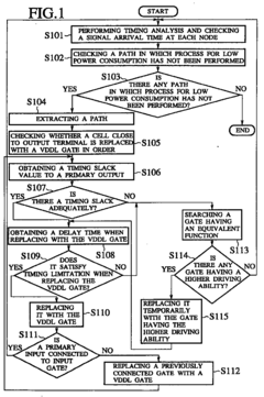
Innovation
- A low power consumption circuit design method that performs timing analysis to identify paths with no timing slack, replacing cells with equivalent function cells having higher driving ability or lower driving ability under a lower voltage power source while ensuring timing constraints are met, thereby reducing power consumption without increasing delay times.
Low power circuit design through judicious module selection
PatentInactiveUS6601230B2
Innovation
- A circuit design system that selects unsigned modules for lower power consumption when permissible, while adhering to design constraints such as gate count and clock speed, and uses signed modules when necessary to maintain desired circuit behavior.


Energy Harvesting Integration for Photocell Circuits
Energy harvesting integration for photocell circuits represents a significant advancement in the design of low-power consumption systems. This approach combines the functionality of photocells with energy harvesting techniques to create self-sustaining, energy-efficient circuits. By harnessing ambient light energy, these integrated systems can operate autonomously for extended periods without relying on external power sources.
The integration process typically involves coupling photocells with energy harvesting modules and power management circuits. Photocells serve as both light sensors and energy generators, converting light into electrical energy. This energy is then captured and stored by the harvesting module, often utilizing supercapacitors or rechargeable batteries. Power management circuits ensure optimal energy utilization, regulating voltage and current flow to meet the system's power requirements.
One of the key advantages of this integration is the potential for perpetual operation in environments with sufficient ambient light. This is particularly beneficial for remote sensing applications, IoT devices, and wearable technologies. By eliminating or reducing the need for battery replacements, these systems can significantly lower maintenance costs and environmental impact.
However, designing effective energy harvesting photocell circuits presents several challenges. The primary concern is maximizing energy conversion efficiency while minimizing power consumption. This requires careful selection of photocell materials, optimizing circuit topology, and implementing advanced power management strategies. Additionally, designers must account for variations in light intensity and ensure system reliability under diverse environmental conditions.
Recent advancements in materials science have led to the development of high-efficiency photocells specifically tailored for energy harvesting applications. These include multi-junction solar cells and organic photovoltaics, which offer improved light absorption and energy conversion rates. Complementing these advancements, innovative circuit designs incorporating ultra-low-power microcontrollers and energy-efficient sensors have further enhanced the viability of integrated photocell energy harvesting systems.
The integration of energy harvesting with photocell circuits also opens up new possibilities for adaptive power management. By implementing intelligent algorithms, these systems can dynamically adjust their power consumption based on available light energy and operational requirements. This adaptive approach ensures optimal performance across varying light conditions and usage scenarios, further extending the system's operational lifespan and reliability.
As the demand for autonomous, low-power devices continues to grow, the integration of energy harvesting in photocell circuits is likely to play an increasingly important role. Future developments in this field may focus on improving energy density, expanding the range of harvestable light spectra, and developing more sophisticated power management techniques. These advancements will further enhance the efficiency and applicability of photocell-based energy harvesting systems across a wide range of industries and applications.
Environmental Impact of Low Power Photocell Solutions
The adoption of low power photocell solutions in circuit design has significant environmental implications, extending beyond energy efficiency to broader ecological considerations. These solutions contribute to reduced energy consumption, which directly translates to lower greenhouse gas emissions associated with power generation. As photocell circuits become more energy-efficient, they require less frequent battery replacements or recharging, leading to a decrease in battery waste and the environmental impact of battery production and disposal.
Low power photocell circuits also play a crucial role in enabling the development of more sustainable IoT devices and sensor networks. By minimizing power requirements, these circuits allow for the deployment of self-powered or energy-harvesting systems, reducing the need for traditional power sources and associated infrastructure. This shift towards energy autonomy in sensing devices contributes to a reduction in the overall carbon footprint of smart city initiatives, environmental monitoring systems, and industrial automation applications.
The environmental benefits of low power photocell solutions extend to the manufacturing process as well. As these circuits require fewer components and simpler designs, they often result in reduced material usage and waste during production. This aligns with principles of sustainable manufacturing and circular economy, promoting resource efficiency and minimizing the environmental impact of electronic device production.
Furthermore, the longevity of devices incorporating low power photocell circuits is typically enhanced due to reduced thermal stress and component wear. This increased lifespan contributes to a decrease in electronic waste, addressing one of the fastest-growing waste streams globally. By extending the operational life of devices, these solutions help mitigate the environmental challenges associated with e-waste disposal and the extraction of raw materials for new device production.
In the context of smart lighting systems and daylight harvesting applications, low power photocell circuits enable more precise control of artificial lighting, leading to significant energy savings in buildings. This not only reduces electricity consumption but also indirectly contributes to lower cooling loads in air-conditioned spaces, further enhancing energy efficiency and reducing the overall environmental impact of built environments.
The cumulative effect of widespread adoption of low power photocell solutions can lead to substantial reductions in global energy demand, particularly in standby power consumption of electronic devices. This aligns with international efforts to combat climate change and achieve sustainable development goals, highlighting the role of innovative circuit design in addressing pressing environmental challenges.
Unlock deeper insights with Patsnap Eureka Quick Research — get a full tech report to explore trends and direct your research. Try now!
Generate Your Research Report Instantly with AI Agent
Supercharge your innovation with Patsnap Eureka AI Agent Platform!