How To Reduce Noise In Photocell Circuits For Precision Sensing
AUG 21, 20259 MIN READ
Generate Your Research Report Instantly with AI Agent
Patsnap Eureka helps you evaluate technical feasibility & market potential.
Photocell Noise Reduction Objectives
The primary objective of reducing noise in photocell circuits for precision sensing is to enhance the signal-to-noise ratio (SNR) and improve the overall accuracy and reliability of measurements. This goal is crucial in various applications where high-precision sensing is required, such as in scientific instruments, medical devices, and industrial control systems.
One key aspect of noise reduction objectives is to minimize the impact of external electromagnetic interference (EMI) on the photocell circuit. This involves implementing effective shielding techniques and optimizing circuit layout to reduce the susceptibility to ambient electromagnetic noise. By isolating the sensitive components and utilizing proper grounding strategies, the influence of external noise sources can be significantly mitigated.
Another important objective is to address the inherent noise generated within the photocell itself. This includes thermal noise, shot noise, and flicker noise, which are intrinsic to semiconductor devices. Developing strategies to minimize these internal noise sources through careful component selection, biasing techniques, and temperature management is essential for achieving high-precision sensing capabilities.
Improving the signal conditioning and amplification stages of the photocell circuit is also a critical objective. This involves designing low-noise amplifiers and implementing advanced filtering techniques to extract the desired signal while suppressing unwanted noise components. The use of precision components and optimized circuit topologies can greatly contribute to reducing noise in the signal path.
Furthermore, the objective of noise reduction extends to the analog-to-digital conversion process, where the goal is to preserve the integrity of the analog signal during digitization. Implementing high-resolution ADCs with appropriate sampling rates and employing techniques such as oversampling and digital filtering can help minimize quantization noise and improve the overall signal quality.
Addressing power supply noise is another crucial objective in photocell noise reduction. Developing clean and stable power supply systems, including voltage regulators and decoupling networks, helps minimize the introduction of noise through power lines and ensures a consistent operating environment for the sensitive photocell circuit.
Lastly, the objective of noise reduction in photocell circuits also encompasses the development of advanced signal processing algorithms and techniques. This includes implementing digital noise cancellation methods, adaptive filtering, and statistical analysis to further enhance the signal quality and extract meaningful information from noisy measurements.
By focusing on these objectives, researchers and engineers can work towards developing highly sensitive and accurate photocell-based sensing systems that push the boundaries of precision measurement capabilities across various fields and applications.
Precision Sensing Market Analysis
The precision sensing market has experienced significant growth in recent years, driven by increasing demand for accurate and reliable measurement technologies across various industries. This market segment encompasses a wide range of applications, including industrial automation, healthcare, automotive, aerospace, and consumer electronics. The global precision sensing market was valued at approximately $15 billion in 2020 and is projected to reach $25 billion by 2025, with a compound annual growth rate (CAGR) of 10.8%.
One of the key factors driving market growth is the rising adoption of Industry 4.0 and IoT technologies, which require high-precision sensors for data collection and analysis. The automotive industry, in particular, has been a major contributor to market expansion, with the increasing integration of advanced driver assistance systems (ADAS) and autonomous driving technologies. These applications demand highly accurate and noise-resistant sensors for optimal performance and safety.
In the healthcare sector, precision sensing technologies are crucial for medical diagnostics, patient monitoring, and drug delivery systems. The COVID-19 pandemic has further accelerated the adoption of remote patient monitoring solutions, creating new opportunities for precision sensing technologies. Additionally, the growing focus on personalized medicine and point-of-care diagnostics is expected to drive demand for miniaturized, high-performance sensors.
The consumer electronics market is another significant driver of precision sensing technology adoption. Smartphones, wearables, and smart home devices increasingly incorporate various sensors for improved functionality and user experience. This trend is expected to continue as consumers demand more advanced features and capabilities from their devices.
Geographically, North America and Europe currently dominate the precision sensing market, owing to their strong industrial base and technological advancements. However, the Asia-Pacific region is expected to witness the highest growth rate in the coming years, driven by rapid industrialization, increasing automotive production, and growing investments in healthcare infrastructure.
Key players in the precision sensing market include Honeywell International Inc., TE Connectivity Ltd., Texas Instruments Inc., and STMicroelectronics N.V. These companies are focusing on developing innovative sensor technologies with improved accuracy, reduced noise, and enhanced reliability to meet the evolving demands of various industries.
Challenges in the precision sensing market include the need for continuous miniaturization, improved energy efficiency, and enhanced noise reduction capabilities. As applications become more demanding, there is a growing need for sensors that can operate reliably in harsh environments and provide accurate measurements even in the presence of electromagnetic interference and other noise sources. Addressing these challenges will be crucial for companies looking to gain a competitive edge in this rapidly evolving market.
Photocell Circuit Noise Challenges
Photocell circuits are widely used in precision sensing applications, but they face significant challenges due to various noise sources that can compromise the accuracy and reliability of measurements. One of the primary sources of noise in these circuits is thermal noise, also known as Johnson-Nyquist noise, which arises from the random thermal motion of charge carriers within resistive components. This type of noise is particularly problematic in high-sensitivity applications where even small fluctuations can lead to significant errors.
Another major challenge is shot noise, which occurs due to the discrete nature of electric charge and the random arrival of photons at the photocell. Shot noise becomes more pronounced at low light levels, making it a critical factor in low-light sensing applications. The impact of shot noise can be particularly severe in applications requiring high dynamic range or precise light intensity measurements.
Electromagnetic interference (EMI) from external sources presents another significant hurdle in photocell circuit design. EMI can couple into the circuit through various mechanisms, including capacitive and inductive coupling, as well as direct radiation. This interference can introduce spurious signals that are difficult to distinguish from the desired photocell output, leading to measurement inaccuracies and reduced system performance.
Flicker noise, also known as 1/f noise, is a low-frequency noise phenomenon that can significantly affect the performance of photocell circuits, especially in DC and low-frequency applications. This type of noise has a power spectral density that is inversely proportional to frequency, making it particularly problematic for long-term stability and precision in sensing applications.
The physical construction and materials used in photocells can also contribute to noise issues. Impurities and defects in semiconductor materials can lead to generation-recombination noise, which is caused by the random generation and recombination of charge carriers. This type of noise can be particularly challenging to mitigate as it is intrinsic to the photocell material.
Circuit design and layout considerations play a crucial role in managing noise in photocell circuits. Parasitic capacitances and inductances in PCB traces and component leads can introduce additional noise and affect the circuit's frequency response. Careful attention to grounding schemes, shielding, and component placement is essential to minimize these effects.
Power supply noise is another significant challenge, as fluctuations in the supply voltage can couple directly into the sensitive photocell circuit. This can manifest as ripple noise from switching power supplies or as random fluctuations due to load variations in the power distribution network.
Addressing these noise challenges requires a multifaceted approach, combining careful circuit design, component selection, and signal processing techniques. Advanced noise reduction strategies, such as chopper stabilization, correlated double sampling, and lock-in amplification, are often employed to achieve the highest levels of precision in photocell sensing applications.
Current Noise Reduction Solutions
01 Noise reduction in photocell circuits
Various techniques are employed to reduce noise in photocell circuits, including filtering, shielding, and signal processing. These methods help to improve the signal-to-noise ratio and enhance the overall performance of the photocell system.- Noise reduction in photocell circuits: Various techniques are employed to reduce noise in photocell circuits, including filtering, shielding, and circuit design optimization. These methods help improve the signal-to-noise ratio and overall performance of photocell-based systems.
- Photocell circuit design for improved sensitivity: Advanced circuit designs are implemented to enhance the sensitivity of photocell circuits. These designs may include amplification stages, feedback loops, and specialized components to detect and process weak light signals more effectively.
- Temperature compensation in photocell circuits: Temperature compensation techniques are incorporated into photocell circuits to maintain consistent performance across varying environmental conditions. This may involve the use of temperature-sensitive components or adaptive circuit designs.
- Integration of photocell circuits in lighting systems: Photocell circuits are integrated into various lighting systems for automatic control and energy efficiency. These circuits can detect ambient light levels and adjust lighting accordingly, optimizing power consumption and user comfort.
- Photocell circuit applications in solar energy systems: Photocell circuits play a crucial role in solar energy systems, including solar panels and solar tracking devices. These circuits are designed to maximize energy harvesting efficiency and adapt to changing light conditions.
02 Circuit design for improved photocell performance
Specialized circuit designs are implemented to enhance photocell performance and minimize noise. These designs may include amplification stages, feedback loops, and compensation networks to optimize signal quality and reduce interference.Expand Specific Solutions03 Integration of noise suppression components
Noise suppression components such as capacitors, inductors, and resistors are integrated into photocell circuits to filter out unwanted signals and reduce electromagnetic interference. These components help to stabilize the circuit and improve its overall noise immunity.Expand Specific Solutions04 Advanced signal processing techniques
Advanced signal processing techniques, including digital filtering, adaptive noise cancellation, and frequency domain analysis, are applied to photocell circuits to enhance signal quality and reduce noise. These methods help to extract meaningful data from noisy environments.Expand Specific Solutions05 Environmental and thermal noise mitigation
Strategies are implemented to mitigate environmental and thermal noise in photocell circuits. These may include temperature compensation, hermetic sealing, and the use of low-noise materials to minimize the impact of external factors on circuit performance.Expand Specific Solutions
Key Players in Photocell Industry
The noise reduction in photocell circuits for precision sensing is a critical technological challenge in the mature optoelectronics industry. The market for high-precision sensing applications is expanding, driven by demands in sectors like automotive, healthcare, and industrial automation. Key players such as Panasonic, Canon, Sony, and STMicroelectronics are investing heavily in R&D to improve sensor performance and reduce noise. The competition is fierce, with companies like OmniVision Technologies and PixArt Imaging also making significant strides. The technology is approaching maturity, but there's still room for innovation in areas like advanced signal processing and novel materials to further enhance sensitivity and reduce noise in photocell circuits.
Panasonic Intellectual Property Management Co. Ltd.
Technical Solution: Panasonic has developed innovative solutions for reducing noise in photocell circuits for precision sensing. Their approach includes the use of advanced CMOS image sensor technologies with built-in noise reduction capabilities[1]. They have implemented a combination of hardware and software techniques, including on-chip noise cancellation circuits and sophisticated digital signal processing algorithms[2]. Panasonic's photocell circuits often incorporate low-noise amplifiers and high-precision analog-to-digital converters to minimize electronic noise[3]. Additionally, they have developed thermal noise reduction techniques by optimizing sensor design and materials, as well as implementing temperature compensation mechanisms[4]. Their latest sensors also feature improved pixel architectures that reduce dark current and increase sensitivity, further enhancing signal-to-noise ratio in low-light conditions[5].
Strengths: Comprehensive noise reduction approach combining hardware and software solutions, expertise in CMOS sensor technology. Weaknesses: May have higher power consumption due to complex noise reduction processing, potential trade-offs between noise reduction and other performance factors.
Canon, Inc.
Technical Solution: Canon has developed advanced noise reduction techniques for photocell circuits in precision sensing applications. Their approach includes the implementation of dual gain architecture in their CMOS sensors, allowing for high dynamic range and low noise performance[1]. Canon has also introduced on-chip noise reduction circuits that perform real-time processing to minimize both temporal and fixed pattern noise[2]. Their sensors often incorporate microlens arrays and backside illumination technology to improve light collection efficiency and reduce noise in low-light conditions[3]. Additionally, Canon has developed proprietary readout circuits with low-noise amplifiers and high-precision ADCs to minimize readout noise[4]. They have also implemented advanced cooling systems in some of their high-end sensors to reduce thermal noise, particularly for long-exposure applications[5].
Strengths: Innovative sensor designs, strong expertise in optics and imaging, comprehensive noise reduction strategies. Weaknesses: Some solutions may be optimized for specific applications (e.g., cameras) and may require adaptation for other precision sensing contexts.
Innovative Noise Filtering Methods
Low-frequency noise removing method and a related CMOS sensing circuit
PatentInactiveEP1024348B1
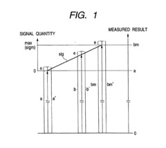
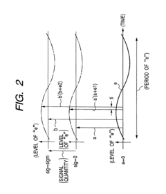
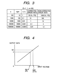
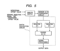
Innovation
- A noise removing method that sets an intentional offset value larger than the sensing objective signal, converts it into digital data, and uses the ratio of the summed sensing objective signal and intentional offset value to reduce low-frequency noise, effectively mitigating the adverse influence of internal noise in CMOS sensing circuits.
Short pulsewidth repetition rate nanosecond transient absorption spectrometer
PatentActiveUS20210172799A1
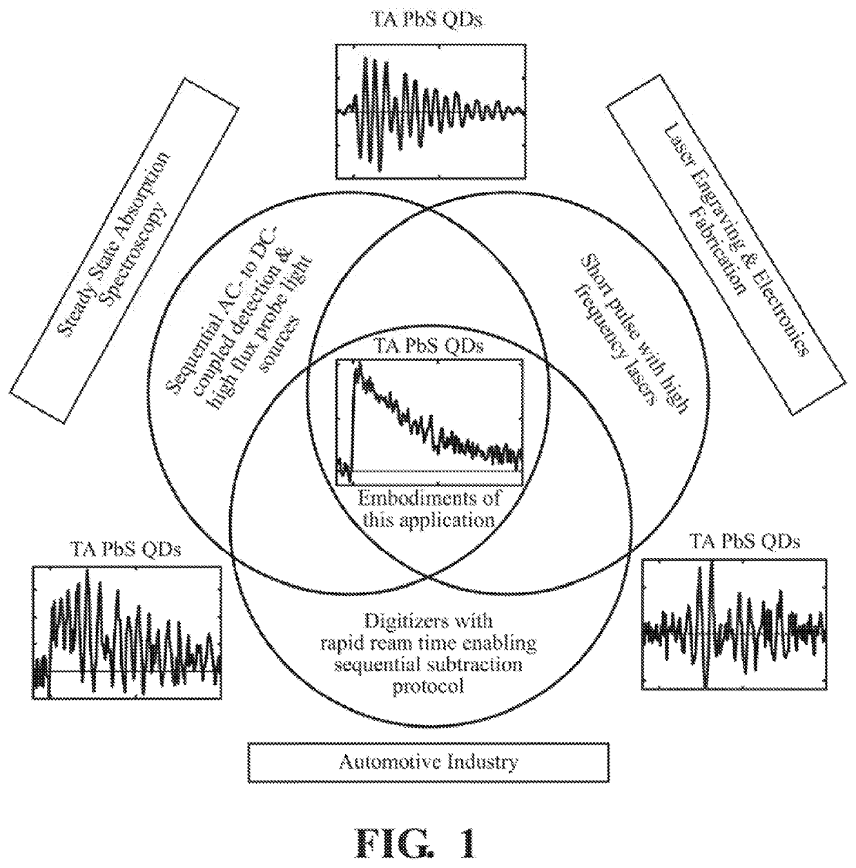
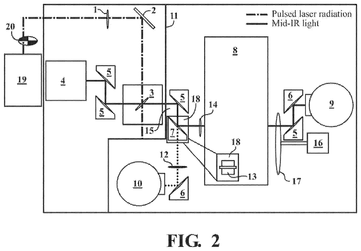
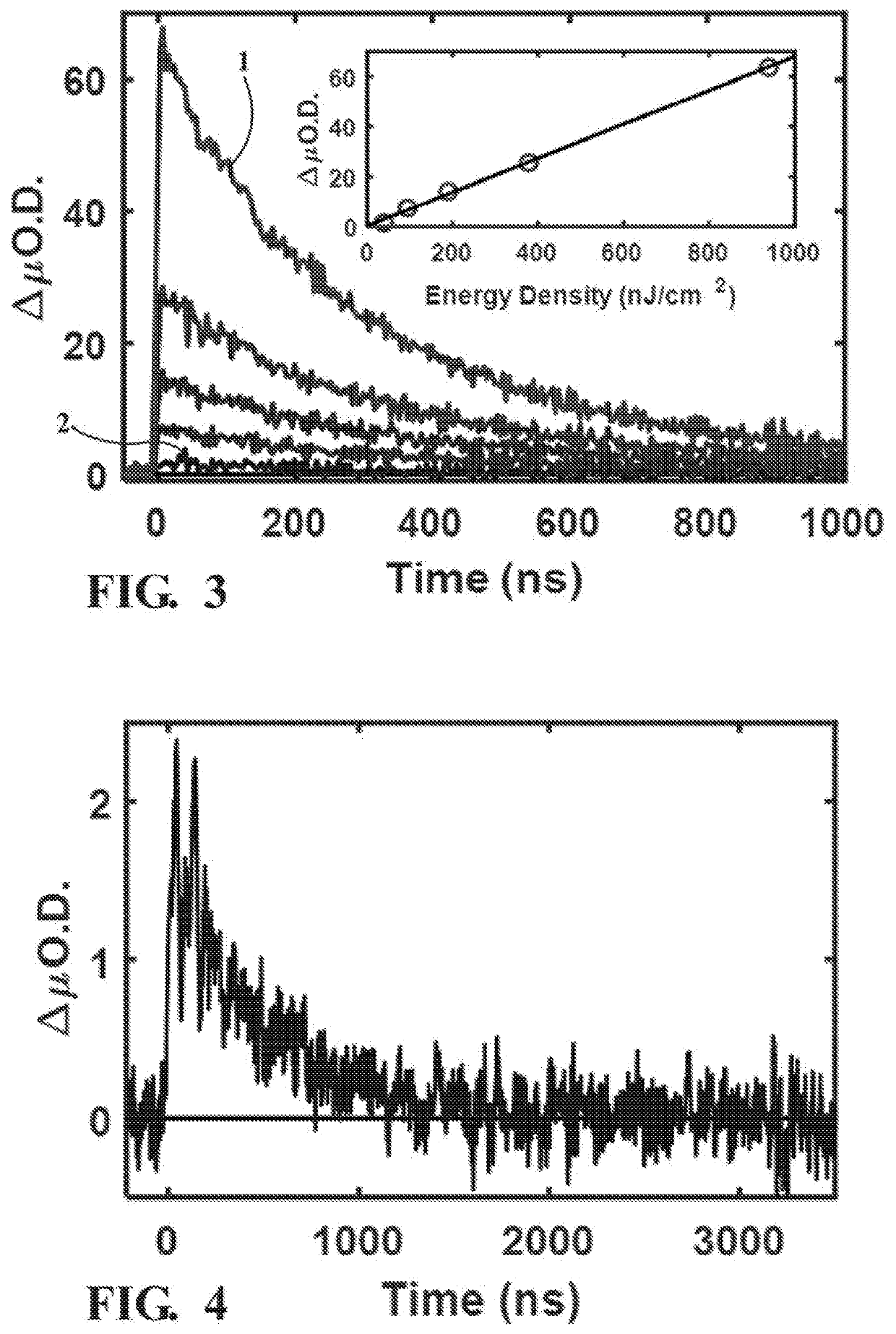
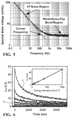
Innovation
- A high-sensitivity nanosecond to millisecond transient absorption spectrometer incorporating a high-frequency excitation pulse, high photon flux probe light beam, DC-coupled detector for synchronous measurement, and a digital oscilloscope with rapid trigger rearm time for sequential noise subtraction protocols, combining three noise cancellation techniques to enhance signal-to-noise ratio.
Electromagnetic Compatibility Standards
Electromagnetic Compatibility (EMC) standards play a crucial role in reducing noise in photocell circuits for precision sensing. These standards ensure that electronic devices can function without causing or being affected by electromagnetic interference (EMI). For photocell circuits, adherence to EMC standards is particularly important due to their sensitivity to light and electrical signals.
The International Electrotechnical Commission (IEC) has established several EMC standards relevant to photocell circuits. IEC 61000 series, specifically IEC 61000-4-3 and IEC 61000-4-6, address immunity to radiated and conducted electromagnetic fields. These standards define test methods and acceptance criteria for electronic equipment, including photocell circuits, to ensure they can operate reliably in the presence of electromagnetic disturbances.
In the United States, the Federal Communications Commission (FCC) regulates EMC through Part 15 of its rules. These regulations set limits on the amount of electromagnetic emissions that electronic devices can produce. For photocell circuits used in precision sensing applications, compliance with FCC Class B limits is often necessary to minimize interference with other nearby electronic equipment.
The European Union's EMC Directive (2014/30/EU) mandates that all electronic equipment sold within the EU must meet specific EMC requirements. This directive ensures that devices, including those incorporating photocell circuits, do not generate excessive electromagnetic disturbances and are not susceptible to such disturbances from other sources.
To meet these standards, designers of photocell circuits must implement various noise reduction techniques. Proper shielding is essential to protect the sensitive components from external electromagnetic fields. This can involve using metal enclosures or conductive coatings to create a Faraday cage around the circuit. Additionally, careful PCB layout design, including the use of ground planes and strategic component placement, can significantly reduce EMI susceptibility.
Filtering is another critical aspect of EMC compliance for photocell circuits. The implementation of EMI filters, such as common-mode chokes and ferrite beads, can attenuate high-frequency noise that may interfere with the circuit's operation. Power supply decoupling capacitors are also crucial for reducing noise on power lines, which can affect the accuracy of photocell measurements.
Compliance with EMC standards not only ensures legal and regulatory requirements are met but also improves the overall reliability and performance of photocell circuits in precision sensing applications. By adhering to these standards, designers can create robust circuits that maintain accuracy even in electromagnetically noisy environments, ultimately leading to more reliable and precise sensing systems.
Environmental Factors in Sensing
Environmental factors play a crucial role in the performance and accuracy of photocell circuits used for precision sensing. These external influences can significantly impact the signal-to-noise ratio, potentially leading to inaccurate measurements and reduced overall system reliability. Temperature fluctuations are one of the primary environmental factors affecting photocell circuits. Changes in ambient temperature can alter the electrical characteristics of semiconductor components, resulting in variations in resistance and current flow. This temperature dependence can introduce thermal noise and drift, compromising the stability of sensor readings over time.
Humidity is another critical environmental factor that can affect photocell circuits. High humidity levels may lead to condensation on circuit components, potentially causing short circuits or corrosion. Additionally, moisture can alter the optical properties of the photocell's surface, affecting its sensitivity and response to light. Proper encapsulation and moisture-resistant coatings are essential to mitigate these effects and ensure consistent performance in varying humidity conditions.
Electromagnetic interference (EMI) from nearby electronic devices or power sources can introduce noise into photocell circuits. This interference can manifest as unwanted signals or distortions in the sensor output, reducing the overall accuracy of the sensing system. Proper shielding techniques, such as Faraday cages or EMI-absorbing materials, can help minimize the impact of electromagnetic interference on sensitive photocell circuits.
Mechanical vibrations and shocks can also affect the performance of photocell circuits, particularly in industrial or automotive applications. These physical disturbances can cause misalignment of optical components or introduce microphonic noise, leading to erroneous sensor readings. Implementing vibration isolation techniques and robust mechanical designs can help mitigate these effects and improve the reliability of photocell-based sensing systems.
Light pollution from artificial sources or ambient light variations can interfere with the intended light measurements of photocell circuits. This is especially problematic in outdoor applications or environments with varying lighting conditions. Implementing optical filters, light baffles, or adaptive gain control mechanisms can help reduce the impact of unwanted light sources and maintain accurate sensing capabilities across different lighting scenarios.
Dust, particulates, and other contaminants in the environment can accumulate on the surface of photocells, affecting their sensitivity and spectral response. Regular maintenance and cleaning procedures are essential to ensure optimal performance of photocell circuits in dusty or contaminated environments. Additionally, incorporating protective covers or self-cleaning mechanisms can help extend the operational life and maintain the accuracy of photocell-based sensing systems in challenging environmental conditions.
Unlock deeper insights with Patsnap Eureka Quick Research — get a full tech report to explore trends and direct your research. Try now!
Generate Your Research Report Instantly with AI Agent
Supercharge your innovation with Patsnap Eureka AI Agent Platform!