How To Miniaturize Photocells For Wearable Light Sensors
AUG 21, 20259 MIN READ
Generate Your Research Report Instantly with AI Agent
Patsnap Eureka helps you evaluate technical feasibility & market potential.
Photocell Miniaturization Background and Objectives
Photocell miniaturization for wearable light sensors represents a critical frontier in the development of advanced wearable technologies. This field has evolved significantly over the past decades, driven by the increasing demand for compact, efficient, and versatile light-sensing devices in various applications, particularly in the wearable technology sector.
The journey of photocell miniaturization began with the invention of the first photoelectric cell in the early 20th century. Since then, continuous advancements in semiconductor technology, materials science, and nanofabrication techniques have paved the way for progressively smaller and more sensitive photocells. The transition from bulky vacuum tube-based photocells to solid-state devices marked a significant milestone in this evolution.
Recent years have witnessed an acceleration in miniaturization efforts, propelled by the rapid growth of the wearable technology market. The integration of light sensors into smartwatches, fitness trackers, and other wearable devices has created a pressing need for photocells that are not only small but also flexible, energy-efficient, and capable of operating under various lighting conditions.
The primary objective of photocell miniaturization for wearable light sensors is to develop ultra-compact photocells that can be seamlessly integrated into wearable devices without compromising functionality or user comfort. This goal encompasses several key aspects, including reducing the physical dimensions of the photocell, enhancing its sensitivity to light, improving energy efficiency, and ensuring compatibility with flexible and stretchable substrates.
Another crucial objective is to achieve multi-functionality within the miniaturized photocell. This involves developing sensors capable of detecting not just light intensity but also spectral information, enabling applications such as UV exposure monitoring or color sensing in wearable devices. Additionally, there is a focus on creating photocells that can operate effectively across a wide range of lighting conditions, from bright sunlight to low-light environments.
The miniaturization efforts also aim to address the challenges of power consumption and heat generation, which are particularly critical in the context of wearable devices with limited battery capacity. Researchers are exploring novel materials and architectures that can improve the quantum efficiency of photocells while minimizing energy loss.
As the field progresses, there is an increasing emphasis on developing fabrication techniques that are scalable and cost-effective, ensuring that miniaturized photocells can be mass-produced for widespread adoption in consumer wearables. This includes exploring new manufacturing processes such as roll-to-roll printing or 3D printing of photosensitive materials.
The ultimate vision for photocell miniaturization in wearable light sensors is to create devices that are virtually imperceptible to the user while providing high-performance light sensing capabilities. This ambitious goal drives ongoing research and development efforts, pushing the boundaries of what is possible in photocell technology and wearable electronics.
Wearable Light Sensor Market Analysis
The wearable light sensor market is experiencing rapid growth, driven by increasing demand for health monitoring devices, smart wearables, and IoT applications. This market segment is expected to expand significantly in the coming years, with a compound annual growth rate (CAGR) projected to be in the double digits through 2028. The rising adoption of fitness trackers, smartwatches, and medical wearables is a key factor fueling this growth.
Consumer awareness of health and wellness, coupled with the growing trend of personalized healthcare, is creating a strong demand for wearable devices equipped with light sensors. These sensors are crucial for various applications, including heart rate monitoring, blood oxygen level detection, and sleep tracking. The miniaturization of photocells for wearable light sensors is particularly important in this context, as it enables the development of more compact, comfortable, and aesthetically pleasing devices.
The market for wearable light sensors spans several industries, including healthcare, fitness, sports, and consumer electronics. In the healthcare sector, there is a growing emphasis on remote patient monitoring and telemedicine, which has been further accelerated by the global pandemic. This has led to increased demand for wearable devices that can accurately measure vital signs and other health parameters using light-based sensors.
In the fitness and sports segments, consumers are increasingly seeking devices that can provide detailed insights into their physical performance and recovery. Light sensors play a crucial role in these applications, measuring metrics such as heart rate variability, oxygen saturation, and even hydration levels. The ability to miniaturize these sensors is critical for creating more versatile and user-friendly wearable devices.
The consumer electronics market is also a significant driver for wearable light sensors, with smartwatches and fitness bands leading the charge. Major tech companies and startups alike are investing heavily in research and development to improve the accuracy and functionality of light-based sensors in their wearable products. This competition is driving innovation in sensor miniaturization and integration techniques.
Geographically, North America and Europe currently dominate the wearable light sensor market, owing to high consumer adoption rates and the presence of major technology companies. However, the Asia-Pacific region is expected to witness the fastest growth in the coming years, driven by increasing disposable incomes, growing health awareness, and the rapid expansion of the consumer electronics industry in countries like China and India.
Challenges in Photocell Miniaturization
The miniaturization of photocells for wearable light sensors presents several significant challenges that researchers and engineers must overcome. One of the primary obstacles is maintaining or improving the sensitivity and efficiency of the photocell as its size decreases. Smaller photocells typically have reduced light-capturing areas, which can lead to diminished performance in terms of light detection and energy conversion.
Another major challenge lies in the materials and fabrication processes used for miniaturization. Traditional silicon-based photocells may not be suitable for extreme miniaturization due to their rigid nature and limitations in thinning processes. This necessitates the exploration of alternative materials, such as organic semiconductors or nanomaterials, which can offer flexibility and ultra-thin profiles but may introduce new complexities in terms of stability and longevity.
The integration of miniaturized photocells into wearable devices poses additional challenges. These include ensuring proper electrical connections, protecting the sensitive components from environmental factors like moisture and mechanical stress, and managing heat dissipation in a confined space. The compact nature of wearable devices also limits the available power supply, requiring the photocells to operate efficiently with minimal energy consumption.
Achieving uniform performance across an array of miniaturized photocells is another significant hurdle. As dimensions shrink, variations in manufacturing processes can lead to inconsistencies in individual cell performance, affecting the overall reliability and accuracy of the light sensing system. This challenge is particularly acute when aiming for high-resolution light detection in wearable applications.
The cost-effectiveness of producing miniaturized photocells at scale presents an economic challenge. Advanced fabrication techniques and materials required for miniaturization can significantly increase production costs, potentially limiting widespread adoption in consumer wearable devices. Balancing performance improvements with cost considerations is crucial for commercial viability.
Lastly, the long-term stability and degradation of miniaturized photocells in wearable environments pose ongoing challenges. Exposure to varying light conditions, temperature fluctuations, and physical stresses can accelerate degradation processes, potentially shortening the operational lifespan of the sensors. Developing robust encapsulation methods and materials that can withstand these conditions without compromising the photocell's performance or size advantages is a critical area of research and development in this field.
Current Miniaturization Techniques for Photocells
01 Miniaturization of photocells
Advancements in photocell technology have led to the development of smaller, more compact designs. These miniaturized photocells offer improved efficiency and can be integrated into various applications where space is limited. The reduced size allows for greater flexibility in device design and placement.- Miniaturization of photocells: Advancements in photocell technology have led to the development of smaller, more compact designs. These miniaturized photocells offer improved efficiency and can be integrated into various applications where space is limited. The reduced size allows for greater flexibility in device design and placement.
- Array configurations of photocells: Photocells can be arranged in arrays to increase their overall sensitivity and performance. These arrays can be designed in various sizes and configurations to suit specific applications. The arrangement of multiple photocells in a compact space allows for improved light detection and signal processing.
- Photocell size optimization for specific applications: The size of photocells can be optimized for specific applications, such as in imaging devices or solar panels. By tailoring the size to the intended use, manufacturers can achieve a balance between performance, power consumption, and overall device dimensions. This optimization process considers factors like sensitivity, response time, and integration with other components.
- Nanotechnology in photocell design: Nanotechnology has enabled the development of extremely small photocells at the nanoscale level. These nano-sized photocells offer unique properties and can be incorporated into advanced materials and devices. The use of nanostructures in photocell design allows for enhanced light absorption and improved efficiency in a smaller footprint.
- Impact of photocell size on performance characteristics: The size of photocells directly influences their performance characteristics, including sensitivity, response time, and spectral range. Smaller photocells may offer faster response times but may have reduced sensitivity, while larger photocells can capture more light but may be slower to respond. Understanding these trade-offs is crucial for selecting the appropriate photocell size for specific applications.
02 Large-area photocells
Some applications require photocells with larger surface areas to capture more light or cover wider areas. These large-area photocells are designed to maximize light collection efficiency and are often used in solar panels, industrial sensors, and architectural applications.Expand Specific Solutions03 Adjustable photocell size
Certain photocell designs incorporate adjustable or modular components, allowing users to customize the size of the photocell based on specific requirements. This flexibility enables optimization for various light conditions and application needs, improving overall system performance.Expand Specific Solutions04 Photocell arrays and matrices
To achieve specific size requirements or enhance functionality, photocells can be arranged in arrays or matrices. These configurations allow for scalable designs and can be tailored to meet various size constraints while maintaining or improving overall light sensitivity and performance.Expand Specific Solutions05 Size optimization for specific applications
Photocell sizes are often optimized for specific applications, such as in cameras, light meters, or automated lighting systems. The size of the photocell is carefully considered to balance factors like sensitivity, response time, and integration with other components, ensuring optimal performance in the intended use case.Expand Specific Solutions
Key Players in Miniature Photocell Development
The miniaturization of photocells for wearable light sensors is in an early development stage, with a growing market driven by increasing demand for wearable technology. The technology is still maturing, with key players like Sony Semiconductor Solutions, Samsung Electronics, and Huawei Technologies leading research efforts. Companies such as FUJIFILM Corp. and Canon, Inc. are leveraging their expertise in imaging technologies to contribute to this field. The competition is intensifying as both established electronics giants and specialized semiconductor firms like Semiconductor Energy Laboratory Co., Ltd. invest in developing smaller, more efficient photocells for integration into wearable devices.
Sony Semiconductor Solutions Corp.
Technical Solution: Sony Semiconductor Solutions Corp. has developed advanced stacked CMOS image sensor technology for miniaturizing photocells. Their approach involves using a 3-layer stacked sensor structure with backside illumination (BSI) and copper-to-copper bonding[1]. This allows for separate optimization of the photodiode layer, pixel transistor layer, and logic circuit layer. The company has achieved pixel sizes as small as 0.8μm while maintaining high sensitivity and low noise[2]. They've also incorporated advanced noise reduction circuits and high-speed signal processing directly on the sensor chip to improve performance in low light conditions[3].
Strengths: Industry-leading miniaturization capabilities, high performance in low light, and integrated processing. Weaknesses: Potentially higher manufacturing costs and complexity compared to traditional CMOS sensors.
Canon, Inc.
Technical Solution: Canon has been developing miniaturized photocell technologies for various applications, including wearable light sensors. Their approach leverages their expertise in image sensor technology, particularly in the development of high-sensitivity, low-noise CMOS sensors. Canon has introduced a 1/3-inch 250-megapixel CMOS sensor with pixels measuring just 1.5μm square, demonstrating their capability in extreme miniaturization[14]. For wearable applications, Canon is exploring the use of organic photoconductive films (OPF) that can be deposited on flexible substrates, allowing for the creation of bendable and stretchable light sensors[15]. Additionally, Canon has developed advanced noise reduction techniques and on-chip analog-to-digital converters to maintain high performance even with smaller pixel sizes[16].
Strengths: Expertise in high-resolution imaging, advanced noise reduction techniques, and flexible sensor technologies. Weaknesses: May face challenges in adapting high-end imaging technologies to low-power wearable applications.
Innovative Approaches in Photocell Size Reduction
Method for manufacturing a photodetector device and photodetector device
PatentWO2024240588A1
Innovation
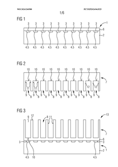
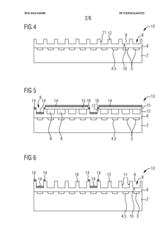
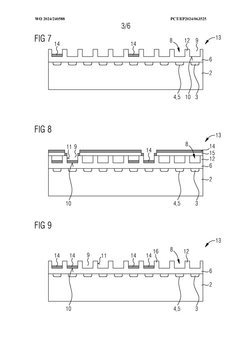
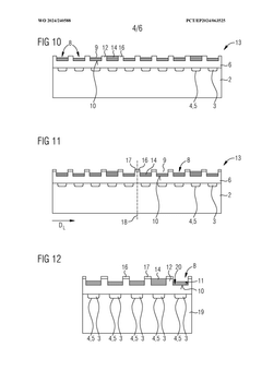
- The method involves using a dielectric wafer with recesses and penetrations that are connected to a functional wafer, allowing for the closer placement of optical filter elements, which are then arranged within these features to create photodetector devices with smaller dimensions by forming cavities and channels that enable efficient detection of specific spectral ranges.
Photoelectric sensor
PatentWO2016157939A1
Innovation
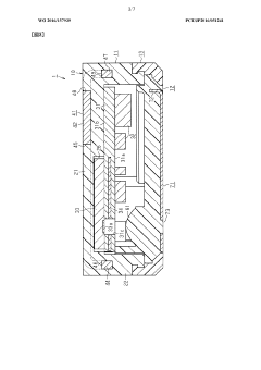
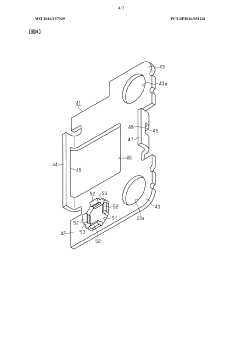
- A miniaturized photoelectric sensor design featuring a resin case with a condensing lens, a circuit board, and a metal plate member insert-molded parallel to the board, with a notch for insulation and folded parts for enhanced integration and strength, along with a shield pattern for electromagnetic shielding, to reduce size and prevent erroneous detection.
Materials Science Advancements for Miniature Photocells
Recent advancements in materials science have paved the way for significant progress in miniaturizing photocells for wearable light sensors. The development of novel nanomaterials and innovative fabrication techniques has been instrumental in this endeavor.
One of the key breakthroughs has been the utilization of two-dimensional materials, such as graphene and transition metal dichalcogenides (TMDs). These materials exhibit exceptional optical and electrical properties at atomic thicknesses, allowing for the creation of ultra-thin and flexible photocells. Graphene, in particular, has shown promise due to its high carrier mobility and broadband light absorption capabilities.
Another important advancement is the development of quantum dot-based photocells. Quantum dots, nanoscale semiconductor particles, can be tuned to absorb specific wavelengths of light, making them highly efficient for targeted light sensing applications. Their small size and versatility make them ideal for integration into wearable devices.
Perovskite materials have also emerged as a promising candidate for miniature photocells. These materials offer high light absorption coefficients and long carrier diffusion lengths, enabling the fabrication of thin-film photocells with excellent performance. Recent research has focused on improving the stability and durability of perovskite-based devices for practical applications.
Advancements in nanofabrication techniques have been crucial in realizing these material innovations. Techniques such as atomic layer deposition (ALD) and molecular beam epitaxy (MBE) allow for precise control over material deposition at the atomic scale, enabling the creation of complex, multi-layered structures with optimized performance.
The integration of organic materials with inorganic semiconductors has led to the development of hybrid photocells. These devices combine the flexibility and low-cost processing of organic materials with the high efficiency of inorganic semiconductors, resulting in photocells that are both compact and high-performing.
Furthermore, the exploration of novel device architectures, such as vertically stacked heterostructures and plasmonic nanostructures, has opened up new possibilities for enhancing light absorption and charge collection in miniature photocells. These designs allow for improved performance without increasing device footprint.
As research in this field continues, we can expect further innovations in materials and fabrication techniques that will push the boundaries of photocell miniaturization. The ongoing development of smart textiles and flexible electronics will likely drive demand for even smaller and more efficient light sensors, spurring continued advancements in materials science for this application.
Energy Efficiency in Miniaturized Photocell Systems
Energy efficiency is a critical factor in the miniaturization of photocell systems for wearable light sensors. As devices become smaller, power consumption becomes increasingly important due to limited battery capacity and the need for extended operational time. Miniaturized photocells face unique challenges in maintaining high energy efficiency while reducing their size.
One of the primary approaches to improving energy efficiency in miniaturized photocell systems is the optimization of the photoactive materials. Researchers are exploring novel semiconductor materials with higher quantum efficiencies and better light absorption properties. These materials can generate more electrical current from the same amount of incident light, thereby increasing the overall energy conversion efficiency of the photocell.
Another key area of focus is the development of advanced power management circuits. These circuits are designed to maximize the power output of the photocell while minimizing energy losses. Techniques such as maximum power point tracking (MPPT) are being adapted for use in miniaturized systems, ensuring that the photocell operates at its optimal voltage and current levels under varying light conditions.
The integration of energy harvesting technologies is also playing a crucial role in enhancing the energy efficiency of miniaturized photocell systems. By combining photocells with other energy harvesting methods, such as thermoelectric or piezoelectric generators, wearable devices can capture energy from multiple sources, reducing their reliance on a single power source and improving overall energy efficiency.
Advancements in low-power electronics and microcontrollers are contributing significantly to the energy efficiency of miniaturized photocell systems. Ultra-low-power microcontrollers can process the signals from the photocell with minimal energy consumption, allowing for more sophisticated light sensing and data processing capabilities without compromising battery life.
Researchers are also exploring novel device architectures to improve energy efficiency. This includes the development of 3D photocell structures that can capture light from multiple angles, increasing the overall light absorption and energy conversion efficiency within a compact form factor.
The use of nanomaterials and nanostructures is another promising avenue for enhancing energy efficiency in miniaturized photocells. Quantum dots, carbon nanotubes, and other nanoscale materials can be engineered to have specific optical and electrical properties, potentially leading to higher efficiency photocells that can operate effectively even at very small scales.
As miniaturization continues, the challenge of thermal management becomes increasingly important for maintaining energy efficiency. Innovative cooling solutions and heat-dissipation techniques are being developed to prevent performance degradation due to heat buildup in compact photocell systems.
Unlock deeper insights with Patsnap Eureka Quick Research — get a full tech report to explore trends and direct your research. Try now!
Generate Your Research Report Instantly with AI Agent
Supercharge your innovation with Patsnap Eureka AI Agent Platform!
