Photocell Sensitivity Optimization For Low-Light Detection
AUG 21, 20259 MIN READ
Generate Your Research Report Instantly with AI Agent
Patsnap Eureka helps you evaluate technical feasibility & market potential.
Photocell Tech Evolution
The evolution of photocell technology for low-light detection has been marked by significant advancements over the past century. Initially, selenium-based photocells were developed in the early 1900s, offering limited sensitivity and reliability. These early devices paved the way for more sophisticated photoelectric sensors.
In the 1950s and 1960s, the introduction of silicon-based photocells revolutionized the field. Silicon photocells demonstrated superior sensitivity and stability compared to their selenium counterparts. This breakthrough led to widespread adoption in various applications, including light meters for photography and automatic street lighting systems.
The 1970s and 1980s saw the emergence of charge-coupled devices (CCDs), which dramatically improved low-light detection capabilities. CCDs offered higher sensitivity and lower noise levels, making them ideal for scientific imaging and astronomy. This technology enabled the capture of faint celestial objects and revolutionized astrophotography.
Complementary metal-oxide-semiconductor (CMOS) sensors emerged as a competitive alternative to CCDs in the 1990s. Initially, CMOS sensors lagged behind CCDs in terms of sensitivity and image quality. However, continuous improvements in CMOS technology, including the development of back-illuminated CMOS sensors, have significantly enhanced their low-light performance.
The early 2000s witnessed the introduction of electron-multiplying CCDs (EMCCDs), which offered unprecedented sensitivity for extremely low-light conditions. EMCCDs found applications in fields such as single-molecule fluorescence microscopy and adaptive optics for large telescopes.
Recent years have seen a focus on enhancing the quantum efficiency of photocells. Developments in materials science and nanotechnology have led to the creation of novel photosensitive materials and structures. Quantum dot-based photocells and perovskite-based sensors have shown promise in pushing the boundaries of low-light detection.
Advancements in signal processing and noise reduction techniques have also played a crucial role in improving photocell sensitivity. Machine learning algorithms and artificial intelligence have been employed to extract meaningful signals from noisy low-light data, further enhancing detection capabilities.
The ongoing trend in photocell technology for low-light detection is towards higher sensitivity, lower noise, and improved spectral response. Researchers are exploring hybrid sensor technologies that combine the strengths of different photocell types. Additionally, there is a growing emphasis on developing photocells that are more energy-efficient and environmentally friendly.
As we look to the future, emerging technologies such as single-photon avalanche diodes (SPADs) and superconducting nanowire single-photon detectors (SNSPDs) hold promise for pushing the boundaries of low-light detection even further. These cutting-edge devices may enable new applications in quantum communication, biomedical imaging, and autonomous systems operating in challenging lighting conditions.
Low-Light Detection Demand
The demand for low-light detection technologies has been steadily increasing across various industries, driven by the need for improved performance in challenging lighting conditions. This growing market requirement stems from applications in security and surveillance, automotive safety systems, scientific research, and consumer electronics.
In the security and surveillance sector, there is a significant push for cameras and sensors capable of capturing clear images in dimly lit environments. This demand is fueled by the need for 24/7 monitoring in both indoor and outdoor settings, where artificial lighting may be limited or impractical. Law enforcement agencies and private security firms are particularly interested in technologies that can enhance their ability to detect and identify potential threats in low-light situations.
The automotive industry has also become a major driver of low-light detection demand. Advanced driver assistance systems (ADAS) and autonomous vehicles require sensors that can operate effectively in a wide range of lighting conditions, including nighttime driving, tunnels, and adverse weather. The ability to detect pedestrians, obstacles, and other vehicles in low-light scenarios is crucial for improving road safety and advancing the development of self-driving technologies.
Scientific research, particularly in fields such as astronomy, biology, and materials science, has created a niche market for highly sensitive low-light detection systems. These applications often involve the observation of faint signals or bioluminescent processes that require extremely sensitive photon detection capabilities. As research in these areas continues to advance, the demand for more sophisticated low-light detection technologies is expected to grow.
In the consumer electronics market, smartphone manufacturers are constantly seeking to improve the low-light performance of their camera systems. This trend is driven by consumer expectations for high-quality photos and videos in all lighting conditions, including dimly lit indoor spaces and nighttime outdoor scenes. The ability to capture clear, noise-free images in low light has become a key differentiator in the competitive smartphone market.
The medical imaging sector also contributes to the demand for low-light detection technologies. Fluorescence microscopy and other diagnostic imaging techniques often require the detection of weak light signals from biological samples. Improved low-light sensitivity can lead to earlier disease detection and more accurate diagnoses, driving the need for advanced photocell technologies in medical equipment.
As urbanization continues and cities implement smart lighting systems, there is a growing need for sensors that can accurately detect ambient light levels to optimize energy consumption. This application requires photocells that can operate reliably in very low light conditions to ensure proper illumination control.
The overall market trend indicates a shift towards more sensitive, faster, and more reliable low-light detection technologies. This demand is pushing manufacturers to invest in research and development to overcome current limitations in photocell sensitivity and explore novel materials and designs that can push the boundaries of low-light detection capabilities.
Current Photocell Limitations
Photocells, also known as photodetectors or light-dependent resistors (LDRs), have been widely used in various applications for light detection and measurement. However, their performance in low-light conditions has been a persistent challenge, limiting their effectiveness in certain scenarios.
One of the primary limitations of current photocells is their relatively low sensitivity in low-light environments. This issue stems from the inherent properties of the semiconductor materials used in their construction, typically cadmium sulfide (CdS) or cadmium selenide (CdSe). These materials exhibit a non-linear response to light intensity, with diminishing sensitivity as light levels decrease.
The signal-to-noise ratio (SNR) of photocells also presents a significant hurdle in low-light detection. As light levels decrease, the electrical signal generated by the photocell becomes weaker, making it increasingly difficult to distinguish from background noise. This problem is exacerbated by thermal noise and other environmental factors, further compromising the accuracy of measurements in low-light conditions.
Another limitation is the slow response time of conventional photocells, particularly in low-light scenarios. The time required for the photocell to reach a stable resistance value after a change in light intensity can be relatively long, especially when transitioning from bright to dim environments. This delay can be problematic in applications requiring rapid detection or measurement of fluctuating light levels.
The spectral sensitivity of current photocells also poses challenges for low-light detection. Most photocells have peak sensitivity in the visible light range, typically around 500-600 nm. However, many low-light applications, such as night vision or astronomical observations, require sensitivity to near-infrared or infrared wavelengths. The limited spectral range of conventional photocells restricts their usefulness in these scenarios.
Temperature dependence is another factor that affects photocell performance in low-light conditions. The resistance of the semiconductor material used in photocells can vary significantly with temperature changes, leading to inaccurate readings and reduced reliability. This temperature sensitivity is particularly problematic in outdoor applications or environments with fluctuating temperatures.
The physical size and form factor of current photocells can also be a limitation for certain low-light detection applications. Miniaturization efforts have been made, but further reductions in size while maintaining or improving sensitivity remain a challenge. This is particularly relevant for applications in compact devices or where space is at a premium.
Lastly, the power consumption of photocells, while generally low, can still be a concern in battery-operated or energy-efficient devices. Improving the energy efficiency of photocells, especially in low-light conditions where they may need to operate for extended periods, is an ongoing area of research and development.
Existing Sensitivity Solutions
01 Improving photocell sensitivity through material selection
Enhancing photocell sensitivity can be achieved by carefully selecting and optimizing the materials used in the photocell construction. This includes using high-quality semiconductors, doping materials, and surface treatments to increase light absorption and charge carrier generation. Advanced materials such as quantum dots or perovskites can also be incorporated to improve sensitivity across a wider spectrum of light.- Improving photocell sensitivity through material selection: Enhancing photocell sensitivity can be achieved by carefully selecting and optimizing the materials used in the photocell construction. This includes using high-quality semiconductors, doping materials, and electrode materials that can increase the efficiency of light absorption and charge carrier generation. Advanced materials such as nanostructures or quantum dots can also be incorporated to improve sensitivity across a wider range of wavelengths.
- Optical design for increased photocell sensitivity: Optimizing the optical design of photocells can significantly improve their sensitivity. This includes implementing anti-reflective coatings, light trapping structures, and specialized lens systems to maximize light collection and minimize losses. Advanced optical designs can also incorporate light concentration techniques to increase the effective light intensity reaching the photosensitive area.
- Electronic signal processing for sensitivity enhancement: Implementing sophisticated electronic signal processing techniques can enhance the overall sensitivity of photocell systems. This includes using low-noise amplifiers, advanced filtering algorithms, and adaptive gain control mechanisms. Digital signal processing techniques can also be employed to improve signal-to-noise ratios and detect weak signals in high-noise environments.
- Temperature compensation and environmental adaptability: Developing temperature compensation mechanisms and improving environmental adaptability can enhance photocell sensitivity across various operating conditions. This involves implementing temperature sensors and feedback loops to adjust the photocell's response based on ambient conditions. Additionally, protective coatings and packaging techniques can be used to shield the photocell from environmental factors that may degrade its performance.
- Multi-junction and spectral optimization techniques: Utilizing multi-junction designs and spectral optimization techniques can improve photocell sensitivity across a broader range of light wavelengths. This approach involves stacking multiple photosensitive layers with different bandgaps or incorporating materials that can efficiently convert a wider spectrum of light into electrical signals. Spectral filters and wavelength-specific coatings can also be used to tailor the photocell's response to specific applications.
02 Optical design for increased light collection
Improving the optical design of photocells can significantly enhance their sensitivity. This involves implementing techniques such as anti-reflective coatings, light trapping structures, and optimized cell geometries to maximize light collection and minimize losses. Micro-lenses or light concentrators can also be used to focus more light onto the active area of the photocell.Expand Specific Solutions03 Electronic signal amplification and processing
Enhancing photocell sensitivity through electronic means involves implementing advanced signal amplification and processing techniques. This can include using low-noise amplifiers, integrating circuits for signal accumulation, and implementing adaptive gain control. Digital signal processing algorithms can also be employed to extract weak signals from background noise.Expand Specific Solutions04 Temperature compensation and environmental control
Photocell sensitivity can be affected by temperature fluctuations and environmental factors. Implementing temperature compensation circuits and environmental control measures can help maintain consistent sensitivity across varying conditions. This may include using thermistors, Peltier cooling elements, or software-based correction algorithms to adjust for temperature-induced variations in photocell response.Expand Specific Solutions05 Multi-junction and spectral optimization
Improving photocell sensitivity across a wide spectral range can be achieved through multi-junction designs and spectral optimization techniques. This involves stacking multiple photocell layers with different bandgaps to capture a broader range of wavelengths. Additionally, implementing spectral filtering or using wavelength conversion materials can help tailor the photocell's response to specific applications or light conditions.Expand Specific Solutions
Key Photocell Manufacturers
The photocell sensitivity optimization for low-light detection market is in a growth phase, driven by increasing demand for advanced sensing technologies across various industries. The global market size is expanding, with projections indicating significant growth in the coming years. Technologically, the field is advancing rapidly, with companies like OmniVision Technologies, Sony Semiconductor Solutions, and Samsung Electronics leading innovation. These firms are developing cutting-edge sensors and imaging solutions, pushing the boundaries of low-light detection capabilities. Other players like Japan Display and Sharp are also contributing to the competitive landscape, focusing on specialized applications and niche markets within the broader photocell sensitivity domain.
OmniVision Technologies, Inc.
Technical Solution: OmniVision has developed advanced CMOS image sensors with enhanced low-light sensitivity. Their PureCel®Plus-S technology utilizes larger pixel sizes (up to 2.0 microns) and improved quantum efficiency to capture more light in dim conditions[1]. They have also implemented a backside-illuminated (BSI) architecture, which increases the amount of light captured compared to front-side illumination[2]. Additionally, OmniVision's Night Vision CameraCubeChip® technology combines an image sensor, processor, and lens in a single compact package, optimized for low-light performance in automotive and security applications[3].
Strengths: Specialized in image sensor technology, wide range of applications from mobile to automotive. Weaknesses: Faces strong competition from larger semiconductor companies, potential limitations in very specialized photocell applications.
Samsung Electronics Co., Ltd.
Technical Solution: Samsung has developed ISOCELL technology for their image sensors, which reduces electrical crosstalk between pixels, improving sensitivity and color fidelity in low-light conditions[7]. Their Dual Pixel technology allows for faster autofocus even in dim environments. Samsung has also implemented Tetracell technology, which combines four pixels into one for better low-light performance[8]. Additionally, they have developed ISOCELL GN1, a 50MP sensor with large 1.2μm-sized pixels and Dual Pixel Pro technology, significantly enhancing low-light capabilities[9].
Strengths: Vertical integration allows for synergy between sensor development and device implementation, strong presence in mobile market. Weaknesses: Less specialized in industrial or scientific photocell applications compared to some competitors.
Core Photocell Innovations
Photo sensor cell, photo sensor and method
PatentWO2022128663A1
Innovation
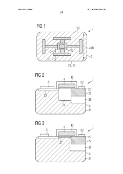
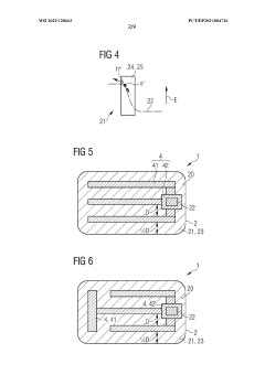
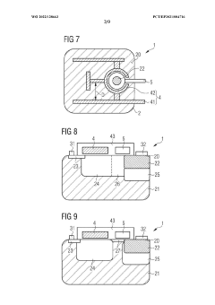
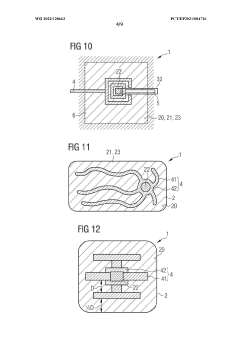
- A photo sensor cell design featuring a collector gate electrode with gate extensions that increase the depletion region, reducing capacitance and enhancing sensitivity, allowing for higher sensitivity and lower noise levels without the need for special manufacturing processes, and can be integrated into standard CMOS processes.
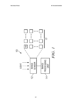
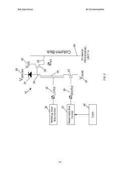
Method and apparatus for increasing pixel sensitivity and dynamic range
PatentWO2016076943A1
Innovation
- A high dynamic range unit cell with a pixel size of 4 microns or below is achieved by utilizing a Metal-Oxide-Semiconductor Capacitor (MOSCap) for both high-sensitivity anti-blooming and low-sensitivity capacitor functions, allowing one anti-bloom switch to be removed and enabling operation in both low and high ambient light situations.
Photocell Material Advances
Recent advancements in photocell materials have significantly contributed to enhancing the sensitivity of photocells for low-light detection applications. These developments have primarily focused on improving the quantum efficiency and reducing the noise levels of photosensitive materials.
One of the most promising materials in this field is perovskite, which has shown exceptional light-harvesting capabilities. Perovskite-based photocells have demonstrated high quantum efficiencies, even in low-light conditions, making them ideal for applications such as indoor light harvesting and low-light imaging. The tunability of perovskite's bandgap allows for optimization across a wide spectrum of light conditions.
Organic photovoltaic materials have also seen significant progress in recent years. These materials offer advantages such as flexibility, low-cost production, and the ability to be tailored for specific wavelengths. Researchers have developed organic compounds with improved charge carrier mobility and reduced recombination rates, leading to enhanced sensitivity in low-light environments.
Quantum dot technology has emerged as another promising avenue for photocell material advancement. Quantum dots can be engineered to absorb light across a broad spectrum, including infrared wavelengths, which is particularly useful for low-light detection. Their size-dependent optical properties allow for precise tuning of absorption and emission characteristics.
Graphene and other two-dimensional materials have shown potential in improving photocell sensitivity. These materials exhibit high carrier mobility and can be integrated with traditional semiconductors to create hybrid structures with enhanced light absorption and charge collection efficiencies.
Nanostructured materials, such as nanowires and nanoparticles, have been incorporated into photocell designs to increase light trapping and absorption. These structures can effectively increase the optical path length within the photocell, leading to improved sensitivity, especially in thin-film designs suitable for low-light applications.
Advancements in doping techniques and surface treatments have also played a crucial role in optimizing photocell materials. Precise control over dopant concentrations and distributions has led to improved charge separation and reduced recombination losses. Surface passivation techniques have been developed to minimize surface defects and enhance charge collection efficiency.
The integration of plasmonic nanostructures with photosensitive materials has shown promise in enhancing light absorption in specific spectral regions. This approach allows for the design of photocells with increased sensitivity to particular wavelengths of interest in low-light detection scenarios.
Quantum Efficiency Metrics
Quantum Efficiency (QE) is a crucial metric for evaluating the performance of photocells in low-light detection applications. It quantifies the effectiveness of a photodetector in converting incident photons into measurable electrical signals. In the context of photocell sensitivity optimization, QE serves as a key indicator of device performance and guides the development of more efficient sensors.
The QE metric is typically expressed as a percentage, representing the ratio of generated electron-hole pairs to the number of incident photons. A higher QE indicates better photon-to-electron conversion efficiency, which is particularly important in low-light conditions where every photon counts. For silicon-based photocells, QE values can range from 30% to over 90%, depending on the wavelength of light and the specific device design.
Measuring QE involves sophisticated techniques such as spectral response analysis and photocurrent measurements. These methods allow researchers to characterize the wavelength-dependent sensitivity of photocells, providing valuable insights into their performance across different parts of the electromagnetic spectrum. This information is essential for optimizing devices for specific applications, such as astronomical observations or night vision systems.
Several factors influence the quantum efficiency of photocells. Surface recombination, bulk recombination, and optical losses are among the primary mechanisms that can reduce QE. Advanced manufacturing techniques, such as surface passivation, anti-reflection coatings, and back-surface field structures, are employed to mitigate these losses and enhance overall QE.
The pursuit of higher QE has led to the development of novel photocell architectures. For instance, back-illuminated sensors, which expose the photosensitive region directly to incoming light, have demonstrated significant improvements in QE compared to traditional front-illuminated designs. Similarly, the integration of light-trapping structures and nanoparticles has shown promise in boosting QE by increasing the optical path length within the device.
Quantum efficiency metrics also play a crucial role in comparing different photocell technologies. For example, when evaluating the potential of emerging materials like perovskites or quantum dots for low-light detection, their QE values are often benchmarked against established silicon-based devices. This comparative analysis helps researchers identify promising new directions for photocell development and guides investment in next-generation sensing technologies.
As the demand for more sensitive low-light detectors continues to grow across various industries, including autonomous vehicles, medical imaging, and environmental monitoring, the importance of quantum efficiency metrics in photocell optimization cannot be overstated. Ongoing research focuses on pushing the boundaries of QE, with the ultimate goal of approaching the theoretical limit of 100% efficiency across a broad spectral range.
Unlock deeper insights with Patsnap Eureka Quick Research — get a full tech report to explore trends and direct your research. Try now!
Generate Your Research Report Instantly with AI Agent
Supercharge your innovation with Patsnap Eureka AI Agent Platform!
