How To Improve Photocell Quantum Efficiency With Material Choices
AUG 21, 20259 MIN READ
Generate Your Research Report Instantly with AI Agent
Patsnap Eureka helps you evaluate technical feasibility & market potential.
Photocell QE Enhancement Goals
Photocell quantum efficiency (QE) enhancement is a critical goal in the development of advanced photovoltaic technologies. The primary objective is to maximize the conversion of incident photons into electrical current, thereby improving the overall performance and efficiency of solar cells. This enhancement aims to address the limitations of current photocell technologies, which often suffer from energy losses due to various factors such as reflection, recombination, and incomplete absorption.
One of the key targets for QE enhancement is to achieve near-unity quantum efficiency across a broad spectrum of wavelengths. This involves optimizing the cell's response to different parts of the solar spectrum, from ultraviolet to near-infrared. By doing so, researchers aim to harness a larger portion of the available solar energy, leading to increased power output and improved cell performance.
Another important goal is to reduce energy losses within the photocell. This includes minimizing surface recombination, enhancing charge carrier collection, and reducing bulk recombination. By addressing these loss mechanisms, researchers seek to ensure that a higher percentage of generated charge carriers contribute to the electrical current, thereby boosting the overall quantum efficiency.
Improving the absorption properties of photocells is also a crucial objective. This involves developing materials and structures that can effectively trap light within the cell, increasing the probability of photon absorption. Techniques such as light trapping, anti-reflection coatings, and nanostructured surfaces are being explored to enhance light absorption and consequently improve quantum efficiency.
Furthermore, researchers are focusing on extending the spectral response of photocells. This includes developing multi-junction cells and exploring novel materials that can efficiently convert a wider range of photon energies into electrical current. By expanding the cell's ability to utilize different parts of the solar spectrum, scientists aim to push the boundaries of quantum efficiency and overall cell performance.
Durability and long-term stability of high-efficiency photocells are also key considerations. The goal is to develop materials and structures that not only exhibit high quantum efficiency but also maintain their performance over extended periods under various environmental conditions. This includes resistance to degradation from UV exposure, temperature fluctuations, and other environmental factors.
Lastly, scalability and cost-effectiveness are crucial aspects of QE enhancement goals. While achieving high quantum efficiency is important, it must be done in a way that is economically viable and suitable for large-scale production. This involves developing materials and fabrication processes that can be scaled up without compromising on efficiency or significantly increasing costs.
Market Demand Analysis
The market demand for improved photocell quantum efficiency through material choices is driven by the growing need for more efficient solar energy conversion and advanced optoelectronic devices. As renewable energy sources gain prominence in the global energy landscape, solar technology continues to be a key focus area. The photovoltaic market is projected to reach significant growth in the coming years, with a compound annual growth rate (CAGR) exceeding 20% in some regions.
The push for higher quantum efficiency in photocells stems from the desire to maximize energy conversion and improve the overall performance of solar panels and other light-sensitive devices. Higher quantum efficiency translates to better light absorption and conversion, leading to increased power output and improved device performance. This demand is particularly strong in the solar energy sector, where even small improvements in efficiency can result in substantial gains in energy production and cost-effectiveness.
In the consumer electronics market, there is a growing trend towards integrating photocells with higher quantum efficiency in smartphones, wearables, and other portable devices. These improved photocells enable better ambient light sensing, more accurate display brightness adjustment, and enhanced camera performance. The Internet of Things (IoT) sector also shows increasing demand for high-efficiency photocells in various sensing applications, contributing to the overall market growth.
The automotive industry is another significant driver of demand for improved photocell quantum efficiency. Advanced driver-assistance systems (ADAS) and autonomous vehicles rely heavily on light sensors and cameras, which benefit from enhanced quantum efficiency. As the automotive sector continues to evolve towards electrification and automation, the demand for high-performance photocells is expected to rise substantially.
In the field of scientific research and medical imaging, there is a constant need for more sensitive light detection systems. Improved quantum efficiency in photocells can lead to breakthroughs in areas such as spectroscopy, microscopy, and diagnostic imaging. This demand from the scientific community drives innovation in material choices for photocells, pushing the boundaries of what is possible in light detection and conversion.
The aerospace and defense sectors also contribute to the market demand for enhanced photocell quantum efficiency. Satellite imaging, remote sensing, and various surveillance applications require highly sensitive light detection capabilities. Improved materials that boost quantum efficiency can lead to better performance in these critical applications, driving investment and research in this area.
As environmental concerns and energy efficiency regulations become more stringent worldwide, there is an increasing focus on developing more efficient energy harvesting technologies. This trend further fuels the demand for photocells with higher quantum efficiency, as they play a crucial role in converting ambient light into usable energy in various applications, from building-integrated photovoltaics to self-powered IoT devices.
Current QE Limitations
Photocell quantum efficiency (QE) is a critical parameter that determines the performance of photoelectric devices. Despite significant advancements in material science and device engineering, current photocells still face several limitations in achieving optimal quantum efficiency. These limitations stem from various factors related to material properties, device structure, and operational conditions.
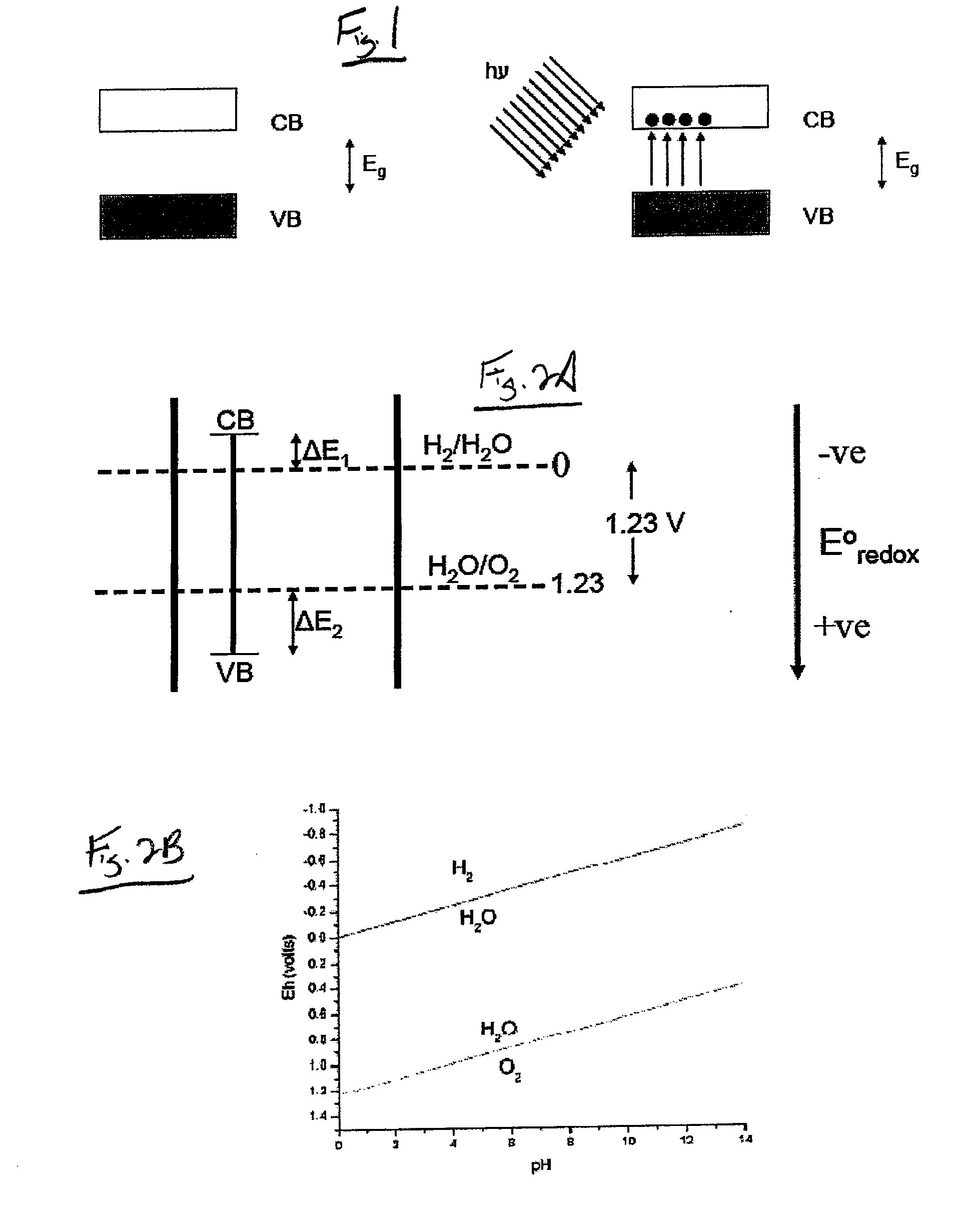
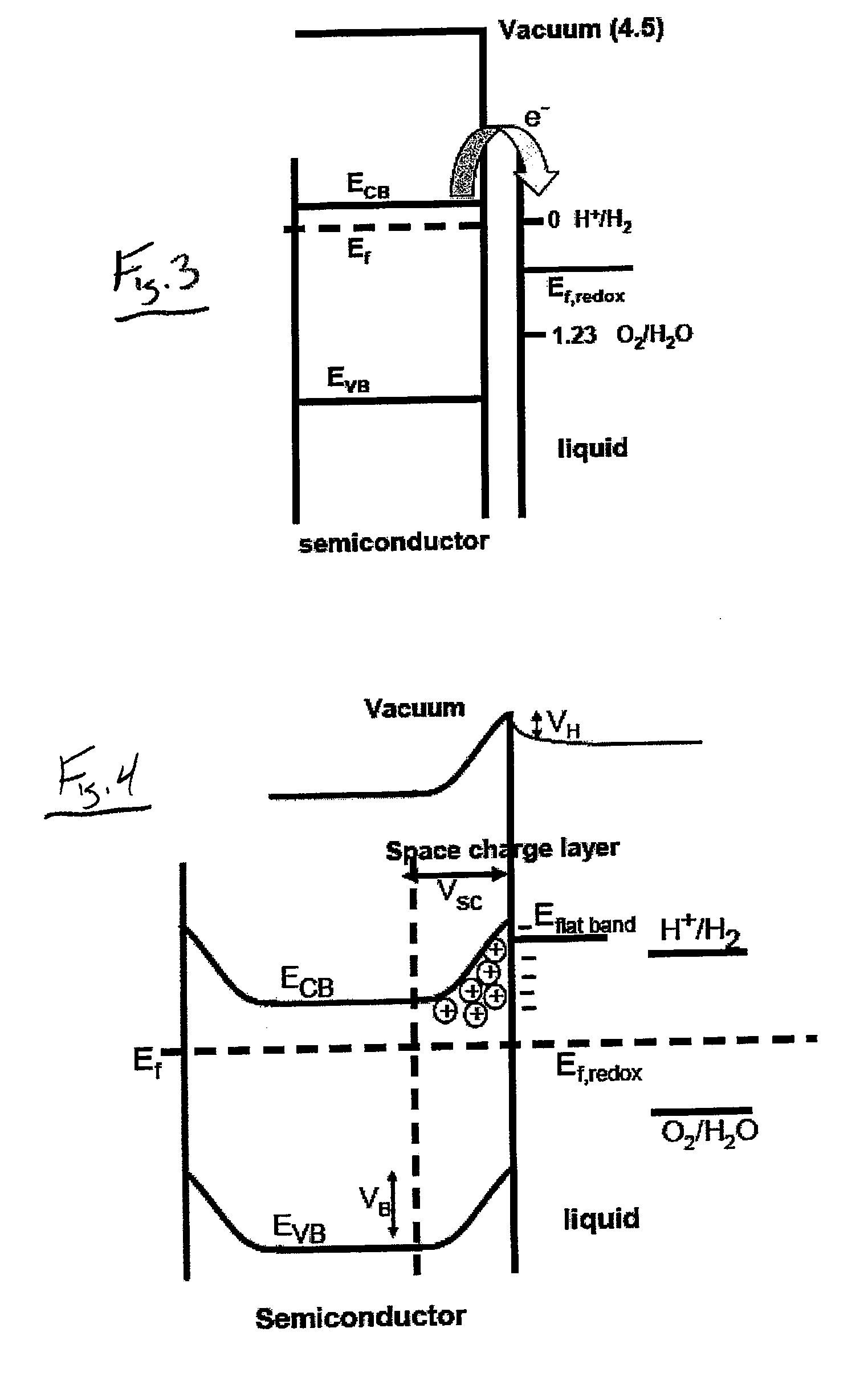
One of the primary constraints on quantum efficiency is the inherent bandgap of semiconductor materials used in photocells. The bandgap determines the range of photon energies that can be effectively absorbed and converted into electrical current. Photons with energies below the bandgap are not absorbed, while those with energies significantly above the bandgap result in energy loss through thermalization. This fundamental limitation, known as the Shockley-Queisser limit, sets a theoretical maximum for single-junction solar cell efficiency.
Surface recombination is another significant factor limiting quantum efficiency. At the material interfaces and surfaces, there is a high concentration of defects and dangling bonds, which act as recombination centers for photogenerated charge carriers. This process reduces the number of carriers that can be collected, thereby decreasing the overall quantum efficiency of the device.
Bulk recombination within the semiconductor material also poses a challenge to achieving high quantum efficiency. Impurities, crystal defects, and grain boundaries in the material can trap charge carriers, leading to non-radiative recombination. This effect is particularly pronounced in polycrystalline and amorphous materials, which are often used in large-scale photovoltaic applications due to their cost-effectiveness.
Optical losses present another set of limitations to quantum efficiency. Reflection at the device surface and incomplete absorption of incident light within the active layer reduce the number of photons available for charge generation. Additionally, parasitic absorption in non-active layers of the device, such as transparent conductive oxides or buffer layers, further diminishes the overall quantum efficiency.
Carrier collection efficiency is also a crucial factor affecting quantum efficiency. The ability to efficiently extract photogenerated carriers before they recombine depends on the device's internal electric field, carrier mobility, and the thickness of the active layer. Balancing these parameters to optimize carrier collection while maintaining sufficient light absorption presents a significant challenge in device design.
Furthermore, the spectral mismatch between the incident light and the absorption spectrum of the photocell material limits the achievable quantum efficiency across the solar spectrum. This mismatch results in inefficient utilization of certain wavelengths, particularly in single-junction devices.
Addressing these limitations requires a multifaceted approach, combining advanced material engineering, novel device architectures, and innovative light management strategies. Overcoming these challenges is crucial for pushing the boundaries of photocell performance and enabling more efficient solar energy conversion technologies.
Existing QE Improvement Solutions
01 Measurement and optimization of quantum efficiency
Various methods and systems are developed to measure and optimize the quantum efficiency of photocells. These techniques involve analyzing the photocell's response to different wavelengths of light and adjusting parameters to improve overall performance. Advanced algorithms and data processing methods are employed to accurately determine quantum efficiency across a wide spectral range.- Measurement and optimization of quantum efficiency: Various methods and systems are developed to measure and optimize the quantum efficiency of photocells. These techniques involve analyzing the photocell's response to different wavelengths of light and adjusting parameters to enhance performance. Advanced algorithms and data processing methods are employed to accurately determine quantum efficiency across a range of operating conditions.
- Materials and structures for improved quantum efficiency: Research focuses on developing novel materials and structures to enhance the quantum efficiency of photocells. This includes the use of nanostructures, advanced semiconductor materials, and innovative device architectures. These improvements aim to increase light absorption, reduce recombination losses, and maximize charge carrier collection.
- Quantum efficiency in specific applications: Photocell quantum efficiency is optimized for specific applications such as solar cells, photodetectors, and imaging devices. Each application requires tailored approaches to maximize performance, considering factors like spectral response, operating temperature, and integration with other components.
- Characterization and testing of quantum efficiency: Advanced characterization and testing methods are developed to accurately assess the quantum efficiency of photocells. These techniques include spectral response measurements, photoluminescence analysis, and in-situ monitoring during device operation. Standardized testing protocols are established to ensure consistency and comparability of results across different research groups and manufacturers.
- Modeling and simulation of quantum efficiency: Computational models and simulation tools are developed to predict and optimize the quantum efficiency of photocells. These models incorporate various physical phenomena, including light absorption, carrier transport, and recombination processes. Simulations help researchers and engineers design more efficient photocells and predict performance under different operating conditions.
02 Enhancing quantum efficiency through material engineering
Research focuses on improving quantum efficiency by engineering novel materials and structures for photocells. This includes developing nanostructured surfaces, implementing multi-junction designs, and exploring new semiconductor compounds. These advancements aim to increase light absorption and charge carrier collection, ultimately boosting the quantum efficiency of photocells.Expand Specific Solutions03 Quantum efficiency characterization techniques
Advanced characterization techniques are developed to accurately measure and analyze the quantum efficiency of photocells. These methods include spectral response measurements, photoluminescence analysis, and time-resolved techniques. Such characterization tools help researchers and manufacturers optimize photocell designs and manufacturing processes.Expand Specific Solutions04 Quantum efficiency in specialized photocell applications
Research explores quantum efficiency improvements in specialized photocell applications, such as space-based solar cells, high-energy particle detectors, and biomedical imaging devices. These applications often require tailored approaches to optimize quantum efficiency under specific operating conditions and environmental constraints.Expand Specific Solutions05 Modeling and simulation of photocell quantum efficiency
Advanced modeling and simulation techniques are developed to predict and optimize the quantum efficiency of photocells. These computational methods allow researchers to explore various design parameters and material combinations virtually, reducing the need for extensive experimental testing and accelerating the development of high-efficiency photocells.Expand Specific Solutions
Key Players in Photocell Industry
The competition landscape for improving photocell quantum efficiency through material choices is characterized by a mature market with significant ongoing research and development. Major players like Sony Semiconductor Solutions, Taiwan Semiconductor Manufacturing Co., and OSRAM Opto Semiconductors are driving innovation in this field. The market is substantial, given the widespread applications of photocells in various industries. Technological advancements are continuous, with companies like Heliatek and Flisom focusing on novel materials such as organic photovoltaics. Academic institutions like Arizona State University and the University of Delaware are also contributing to research efforts, indicating a collaborative ecosystem between industry and academia in pushing the boundaries of photocell efficiency.
Sony Group Corp.
Technical Solution: Sony has developed advanced stacked CMOS image sensor technology to improve photocell quantum efficiency. Their Exmor RS sensors utilize a backside-illuminated (BSI) structure with on-chip lens technology to maximize light capture[1]. The company has also implemented copper-to-copper bonding to create a multi-layer stacked sensor design, allowing for larger photodiodes and more efficient light collection[2]. Additionally, Sony has explored the use of organic photoconductive films (OPF) to enhance sensitivity in specific wavelength ranges, particularly in the near-infrared spectrum[3]. These innovations have led to sensors with quantum efficiencies exceeding 80% across visible wavelengths[4].
Strengths: Industry-leading sensor technology, high quantum efficiency, and versatile applications. Weaknesses: Higher production costs and potential for increased complexity in manufacturing processes.
Soitec SA
Technical Solution: Soitec has focused on improving photocell quantum efficiency through advanced substrate engineering. Their Smart Cut technology enables the production of ultra-thin, high-quality silicon-on-insulator (SOI) wafers, which serve as an excellent base for high-performance photovoltaic cells[1]. By optimizing the thickness and crystal orientation of the top silicon layer, Soitec enhances light absorption and carrier collection efficiency[2]. The company has also developed gallium nitride-on-silicon (GaN-on-Si) substrates, which show promise for high-efficiency optoelectronic devices[3]. Soitec's engineered substrates have demonstrated quantum efficiencies of up to 46% in multi-junction solar cells, significantly higher than traditional silicon cells[4].
Strengths: Expertise in substrate engineering, potential for high-efficiency multi-junction cells. Weaknesses: Higher material costs, limited to specific applications requiring advanced substrates.
Core Innovations in Materials
Photoelectric conversion element, method for measuring same, solid-state imaging element, electronic device, and solar cell
PatentWO2017163923A1
Innovation
- Incorporating charge blocking layers, such as electron and hole blocking layers, with specific ionization potential and electron affinity differences relative to the adjacent electrode materials, and optimizing their positions and thicknesses to create a steep potential gradient within the photoelectric conversion layer, thereby enhancing quantum efficiency and reducing dark current.


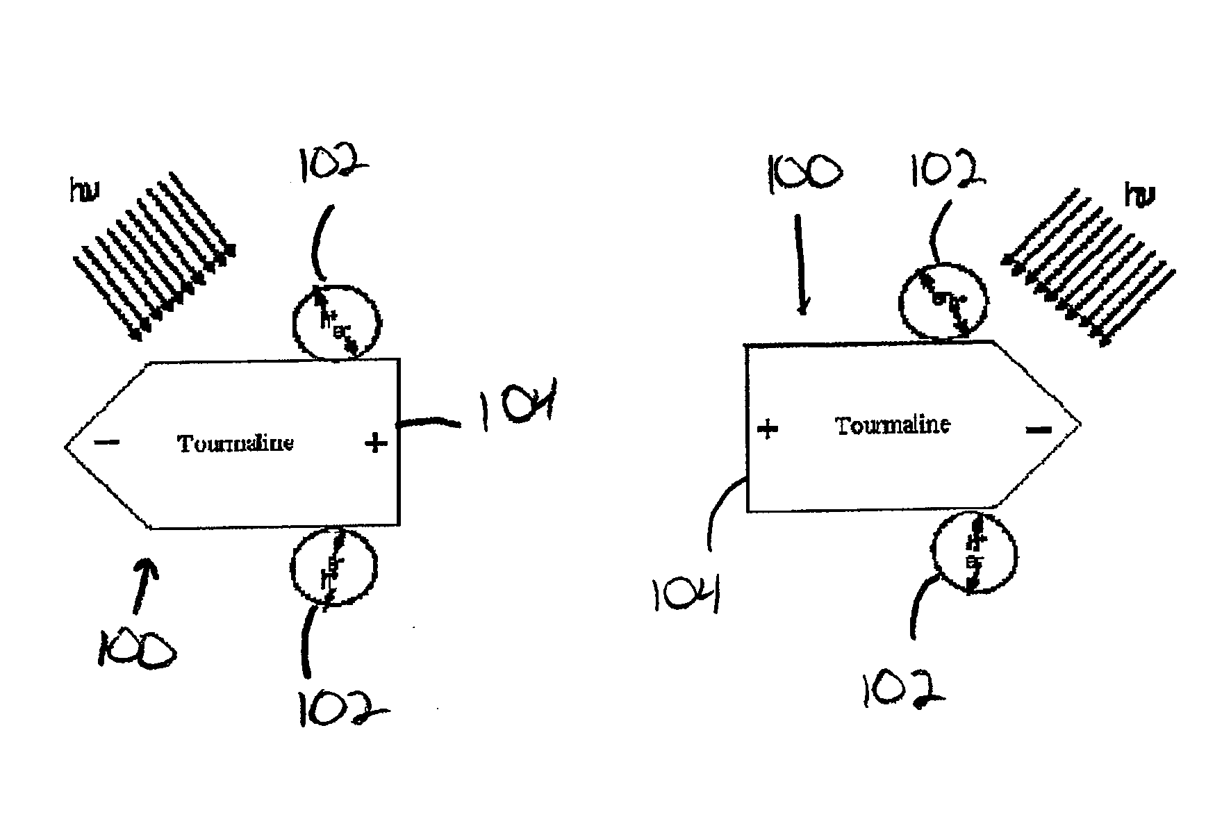
Photocatalyst Having Improved Quantum Efficiency and Method for Use in Photocatalytic and Photosynthetic
PatentInactiveUS20080223713A1
Innovation
- Integrating titania with polar minerals like tourmaline or quartz, which enhance electron-hole pair separation through surface electrical fields, increasing the quantum efficiency and allowing for visible light activation.
Environmental Impact Assessment
The environmental impact of improving photocell quantum efficiency through material choices is a critical consideration in the development and implementation of solar energy technologies. As the demand for more efficient solar cells grows, it is essential to assess the potential environmental consequences of new materials and manufacturing processes.
One of the primary environmental benefits of enhancing photocell quantum efficiency is the potential reduction in the overall material requirements for solar panel production. Higher efficiency cells can generate more electricity from a smaller surface area, potentially decreasing the amount of raw materials needed and reducing the environmental footprint of solar installations.
However, the introduction of new materials to improve quantum efficiency may also present environmental challenges. Some advanced materials, such as rare earth elements or complex nanostructures, may require energy-intensive extraction and processing methods. The production of these materials could lead to increased greenhouse gas emissions, water pollution, or habitat disruption if not carefully managed.
The lifecycle assessment of new photocell materials is crucial in determining their overall environmental impact. This includes evaluating the energy and resources required for material production, the potential for recycling or reuse at the end of the cell's life, and any hazardous waste generated during manufacturing or disposal processes.
Improved quantum efficiency may also contribute to the reduction of toxic materials used in traditional solar cell production. For instance, if new materials can achieve higher efficiencies without relying on heavy metals like cadmium or lead, it could significantly reduce the environmental risks associated with solar panel manufacturing and disposal.
The long-term durability and stability of new materials used to enhance quantum efficiency are also important environmental considerations. Materials that extend the operational lifespan of solar cells can reduce the frequency of replacements, thereby minimizing waste generation and the need for new resource extraction.
Furthermore, the potential for these advanced materials to improve the performance of solar cells in diverse environmental conditions could expand the geographical range of solar energy adoption. This could lead to a broader displacement of fossil fuel-based energy sources, resulting in significant reductions in greenhouse gas emissions and air pollution on a global scale.
It is also important to consider the potential impacts on local ecosystems where large-scale solar installations using these new materials might be deployed. While improved efficiency could reduce the land area required for solar farms, the introduction of novel materials into the environment should be carefully monitored for any unforeseen ecological effects.
Cost-Benefit Analysis of Materials
The cost-benefit analysis of materials for improving photocell quantum efficiency is a critical aspect of advancing solar cell technology. Different materials offer varying levels of performance, durability, and cost-effectiveness, which must be carefully evaluated to determine the most suitable options for specific applications.
Silicon remains the most widely used material for photovoltaic cells due to its abundance, well-established manufacturing processes, and relatively low cost. However, its theoretical efficiency limit of around 29% has prompted research into alternative materials. Gallium arsenide (GaAs) offers higher efficiency potential, with single-junction cells reaching up to 29.1% efficiency, but at a significantly higher cost. The increased performance must be weighed against the substantial increase in production expenses.
Perovskite materials have emerged as a promising alternative, demonstrating rapid efficiency improvements in recent years. Their low-cost production methods and potential for high efficiency make them an attractive option. However, stability issues and the use of lead in some formulations present challenges that must be addressed. The cost-benefit analysis must consider the potential for further efficiency gains against the need for additional research and development to overcome these limitations.
Multi-junction cells, which combine different materials to capture a broader spectrum of light, offer the highest efficiencies but come with increased complexity and cost. For example, triple-junction cells using materials like gallium indium phosphide, gallium arsenide, and germanium can achieve efficiencies over 40% but are primarily used in specialized applications such as space solar panels due to their high cost.
Emerging materials like quantum dots and organic photovoltaics present opportunities for low-cost, flexible solar cells. While their efficiencies are currently lower than traditional silicon cells, their potential for cost-effective large-scale production and unique applications in building-integrated photovoltaics make them worthy of consideration in the cost-benefit analysis.
The evaluation must also account for the long-term performance and degradation rates of different materials. Silicon cells typically have a lifespan of 25-30 years with minimal efficiency loss, while newer materials may have shorter lifespans or faster degradation rates. This factor significantly impacts the overall cost-effectiveness of a material choice over the lifetime of a solar installation.
Manufacturing scalability is another crucial consideration. Materials that offer high efficiency in laboratory settings may face challenges in large-scale production, potentially offsetting their performance advantages with increased costs. The analysis should include the potential for economies of scale and the likelihood of future cost reductions as manufacturing processes improve.
Unlock deeper insights with Patsnap Eureka Quick Research — get a full tech report to explore trends and direct your research. Try now!
Generate Your Research Report Instantly with AI Agent
Supercharge your innovation with Patsnap Eureka AI Agent Platform!