How to Enhance Coupling Coefficient Using Composite Nanostructures
AUG 27, 202510 MIN READ
Generate Your Research Report Instantly with AI Agent
Patsnap Eureka helps you evaluate technical feasibility & market potential.
Composite Nanostructure Coupling Enhancement Background and Objectives
The coupling coefficient is a critical parameter in various nanoscale systems, determining the efficiency of energy transfer between different components. Over the past decade, the field of nanophotonics and plasmonics has witnessed significant advancements in manipulating light-matter interactions at the nanoscale. Composite nanostructures, which combine multiple materials or geometries, have emerged as promising platforms for enhancing coupling coefficients beyond what is achievable with single-material structures.
The evolution of this technology can be traced back to early work on plasmonic nanoparticles, which demonstrated enhanced electromagnetic field confinement. This was followed by the development of metamaterials with engineered electromagnetic properties, and more recently, hybrid nanostructures that leverage the complementary properties of different materials. The progression reflects a shift from passive optical components to actively tunable systems with unprecedented control over light-matter interactions.
Current technological trends point toward multifunctional composite nanostructures that can simultaneously enhance coupling while providing additional functionalities such as sensing, catalysis, or information processing. The integration of quantum materials with traditional plasmonic structures represents another frontier, potentially enabling quantum-enhanced coupling mechanisms.
The primary objective of enhancing coupling coefficients using composite nanostructures is to overcome the fundamental limitations imposed by conventional materials and geometries. Specifically, we aim to achieve coupling coefficients exceeding 0.9 in practical systems, which would enable near-perfect energy transfer efficiency for applications in quantum information processing, energy harvesting, and ultrasensitive detection.
Secondary objectives include developing scalable fabrication methods for these composite nanostructures, ensuring their stability under various operating conditions, and creating design principles that can be applied across different application domains. The ability to dynamically tune the coupling coefficient in response to external stimuli represents another important goal.
From a broader perspective, enhanced coupling coefficients could revolutionize numerous technologies, from quantum computing to renewable energy. By enabling more efficient light-matter interactions, these composite nanostructures could lead to breakthroughs in photovoltaics, quantum communication networks, and nanoscale sensing platforms with unprecedented sensitivity.
The technical challenges in this field are substantial, requiring interdisciplinary approaches that combine insights from materials science, photonics, quantum mechanics, and nanofabrication. However, recent theoretical and experimental advances suggest that significant improvements in coupling coefficients are within reach through careful design and optimization of composite nanostructures.
Market Applications and Demand Analysis for Enhanced Coupling Systems
The enhanced coupling coefficient technology using composite nanostructures addresses critical market needs across multiple industries. The wireless power transfer market, valued at $4.5 billion in 2022, is projected to reach $13.4 billion by 2027, with a compound annual growth rate of 24.6%. This growth is primarily driven by increasing adoption of electric vehicles, wearable electronics, and IoT devices that benefit from efficient wireless charging solutions.
In the telecommunications sector, improved coupling coefficients directly impact signal integrity and data transmission rates. With global data consumption increasing at approximately 30% annually, there is substantial demand for technologies that can enhance bandwidth efficiency without requiring complete infrastructure overhauls. Composite nanostructure-based coupling systems offer a cost-effective solution to this challenge.
Medical device manufacturers represent another significant market segment, with particular interest in implantable devices that require efficient power transfer through biological tissues. The global implantable medical devices market, valued at $96.6 billion in 2022, faces persistent challenges related to power delivery and device longevity that enhanced coupling technologies could address.
Consumer electronics manufacturers are increasingly incorporating wireless charging capabilities into their product ecosystems. Market research indicates that 78% of smartphone users consider wireless charging an important feature when purchasing new devices. Enhanced coupling efficiency directly translates to faster charging times and improved user experience, creating substantial competitive advantages.
Industrial automation systems benefit from improved coupling in sensor networks and power delivery to remote components. The industrial IoT market, growing at 22.8% annually, requires reliable power and data transmission in challenging environments where traditional wiring solutions are impractical or hazardous.
Quantum computing research facilities have expressed interest in advanced coupling technologies for maintaining quantum coherence between components. While this represents a smaller market segment currently, it has significant growth potential as quantum computing moves toward commercial viability.
The automotive sector shows particularly strong demand growth, with electric vehicle manufacturers seeking more efficient wireless charging solutions for both stationary and dynamic charging scenarios. Enhanced coupling efficiency directly impacts charging speed and convenience, addressing key consumer adoption barriers.
Defense and aerospace applications require coupling systems that maintain performance under extreme conditions and electromagnetic interference. These specialized applications command premium pricing despite lower volume requirements, representing a lucrative niche market for advanced coupling technologies.
Current Limitations and Technical Challenges in Nanostructure Coupling
Despite significant advancements in nanostructure coupling technologies, several critical limitations and technical challenges persist that hinder the optimization of coupling coefficients in composite nanostructures. The fundamental challenge lies in the precise control of electromagnetic interactions at the nanoscale, where quantum effects and surface phenomena dominate conventional physics principles.
Material interface management presents a significant obstacle, as the coupling efficiency drastically decreases at boundaries between different nanomaterials. Current fabrication techniques struggle to create atomically smooth interfaces, resulting in scattering losses and reduced coupling coefficients. These imperfections introduce unpredictable phase shifts and energy dissipation that compromise system performance.
Dimensional constraints further complicate coupling enhancement efforts. As structures approach the nanoscale, the coupling coefficient becomes increasingly sensitive to minute variations in geometry and spacing. Current lithography and deposition techniques have reached precision limits of approximately 5-10 nm, which is insufficient for optimal coupling in many advanced applications requiring sub-nanometer precision.
Thermal stability represents another critical challenge. Nanostructures exhibit significant thermal expansion coefficients that can alter coupling distances during operation. Temperature fluctuations as small as 5°C can cause dimensional changes sufficient to dramatically reduce coupling efficiency, particularly in resonant systems where performance depends on precise spatial relationships.
Environmental sensitivity poses additional difficulties, as exposure to oxygen, moisture, or other atmospheric components can alter the surface properties of nanostructures. This surface degradation directly impacts coupling performance, with studies showing coupling coefficient reductions of up to 40% after just 48 hours of environmental exposure in unprotected systems.
Scalability remains problematic for practical applications. While laboratory demonstrations have achieved impressive coupling coefficients in carefully controlled environments, translating these results to mass-production has proven challenging. The yield rates for high-performance coupled nanostructures typically fall below 30% using current manufacturing techniques.
Measurement and characterization limitations further impede progress. Accurately measuring coupling coefficients in complex nanostructures requires sophisticated equipment and techniques that are not widely accessible. The lack of standardized measurement protocols also makes it difficult to compare results across different research groups and approaches.
Addressing these challenges requires interdisciplinary approaches combining advances in materials science, nanofabrication, computational modeling, and measurement technologies. Recent research suggests that hybrid approaches incorporating both top-down and bottom-up fabrication methods may offer promising pathways to overcome current limitations.
State-of-the-Art Composite Nanostructure Design Approaches
01 Electromagnetic coupling in nanostructure composites
Composite nanostructures can be designed with specific electromagnetic coupling coefficients to control energy transfer between components. These structures utilize various materials and geometries to achieve desired coupling effects, enabling applications in sensors, energy harvesting, and signal processing. The coupling coefficient can be tuned by adjusting the distance between nanostructures, material composition, and structural parameters to optimize performance for specific electromagnetic frequencies.- Electromagnetic coupling in composite nanostructures: Composite nanostructures can be designed with specific electromagnetic coupling coefficients to control energy transfer between components. These structures utilize various materials and geometries to achieve desired coupling effects, enabling applications in sensors, energy harvesting, and signal processing. The coupling coefficient can be tuned by adjusting the distance between nanostructures, material composition, and structural parameters to optimize performance for specific electromagnetic frequencies.
- Quantum coupling effects in nanoscale materials: Quantum coupling effects play a significant role in composite nanostructures, where quantum confinement and tunneling phenomena influence the coupling coefficient. These quantum effects can be leveraged to create novel electronic and optical properties in nanomaterials. By controlling the quantum coupling between nanoparticles, quantum dots, or other nanoscale components, researchers can develop advanced materials with enhanced functionality for quantum computing, photonics, and other applications.
- Thermal and mechanical coupling in nanocomposites: Composite nanostructures exhibit unique thermal and mechanical coupling behaviors that affect their overall performance. The coupling coefficient between different materials in these structures determines heat transfer efficiency, mechanical strength, and structural integrity. By engineering the interfaces between nanomaterials, researchers can optimize thermal conductivity, mechanical resilience, and other physical properties for applications in thermal management, structural materials, and energy conversion systems.
- Optical coupling in photonic nanostructures: Optical coupling coefficients in composite nanostructures determine how efficiently light can be transferred, guided, or manipulated between different components. These structures can be designed with specific geometries and material compositions to achieve desired optical coupling effects for applications in photonics, optical computing, and sensing. By controlling the optical coupling coefficient through precise fabrication techniques, researchers can develop advanced photonic devices with enhanced performance characteristics.
- Fabrication methods for controlling coupling coefficients: Various fabrication techniques have been developed to precisely control coupling coefficients in composite nanostructures. These methods include chemical synthesis, lithographic patterning, self-assembly, and atomic layer deposition, which enable the creation of complex nanostructures with tailored coupling properties. By optimizing fabrication parameters, researchers can achieve desired coupling coefficients between different components of the nanostructure, leading to improved performance in electronic, optical, and sensing applications.
02 Quantum coupling effects in semiconductor nanostructures
Semiconductor-based composite nanostructures exhibit quantum coupling effects that can be characterized by specific coupling coefficients. These structures leverage quantum confinement and tunneling phenomena to create unique electronic and optical properties. By controlling the coupling coefficient through precise fabrication techniques, these nanostructures can be optimized for applications in quantum computing, photonics, and advanced electronic devices.Expand Specific Solutions03 Thermal and phononic coupling in nanocomposites
Thermal energy transfer in composite nanostructures is governed by coupling coefficients that describe phonon interactions between different materials. These structures can be engineered to control thermal conductivity, phonon transport, and heat dissipation properties. By manipulating the coupling coefficient through interface engineering and material selection, these nanocomposites can be optimized for thermoelectric applications, thermal management systems, and energy conversion devices.Expand Specific Solutions04 Optical coupling in photonic nanostructures
Photonic composite nanostructures utilize coupling coefficients to control light-matter interactions and energy transfer between components. These structures can manipulate optical properties such as absorption, emission, and scattering through engineered coupling effects. By optimizing the coupling coefficient through precise control of nanostructure geometry, spacing, and material composition, enhanced performance can be achieved in applications including photovoltaics, optical sensors, and photonic integrated circuits.Expand Specific Solutions05 Fabrication methods for controlled coupling in nanostructures
Advanced fabrication techniques enable precise control over coupling coefficients in composite nanostructures. These methods include atomic layer deposition, molecular beam epitaxy, and self-assembly processes that allow for nanometer-scale precision in creating interfaces between different materials. By controlling the fabrication parameters, researchers can tune the coupling coefficient to achieve specific functional properties, enabling customized nanostructures for various applications in electronics, photonics, and energy technologies.Expand Specific Solutions
Leading Research Groups and Industrial Players in Nanostructure Coupling
The field of enhancing coupling coefficients using composite nanostructures is currently in a growth phase, with significant research momentum but still evolving toward commercial maturity. The global market for nanomaterials is expanding rapidly, projected to reach $14.7 billion by 2025, with composite nanostructures representing a high-value segment. Leading academic institutions like MIT, Tsinghua University, and Cornell University are driving fundamental research, while companies including Boeing, Airbus, and Toyota are exploring applications in aerospace and automotive sectors. Research collaborations between institutions like Fraunhofer-Gesellschaft and CNRS are accelerating technological development. The field is transitioning from laboratory research to early commercial applications, with significant potential for industries requiring enhanced electromagnetic coupling and energy transfer efficiency.
Massachusetts Institute of Technology
Technical Solution: MIT has pioneered advanced approaches to enhance coupling coefficients using composite nanostructures through their innovative work with metamaterials and plasmonic nanostructures. Their research focuses on creating engineered nanocomposites with precisely controlled geometries that can significantly amplify electromagnetic coupling. MIT researchers have developed multilayered metal-dielectric nanostructures that demonstrate coupling coefficient enhancements of up to 300% compared to conventional materials. Their approach involves strategic placement of plasmonic nanoparticles within dielectric matrices to create resonant coupling effects that maximize energy transfer efficiency. MIT has also explored the use of quantum dots embedded in photonic crystal structures to achieve strong coupling regimes, where the coupling coefficient exceeds the decay rates of the individual components, enabling coherent energy exchange. Their recent work has expanded to include topological photonic structures that provide robust coupling mechanisms resistant to fabrication imperfections and environmental perturbations.
Strengths: Exceptional fundamental research capabilities with access to state-of-the-art nanofabrication facilities; interdisciplinary approach combining physics, materials science, and engineering; strong track record of translating theoretical concepts into practical applications. Weaknesses: Solutions often require complex fabrication techniques that may be challenging to scale for industrial production; high-precision requirements may increase costs for commercial implementation.
Korea Advanced Institute of Science & Technology
Technical Solution: KAIST has developed sophisticated approaches to enhance coupling coefficients using composite nanostructures through their groundbreaking research in nanophotonics and metamaterials. Their primary innovation lies in creating precisely engineered nanostructures with tailored optical and electronic properties that maximize coupling efficiency. KAIST researchers have successfully demonstrated hybrid metal-semiconductor nanostructures that achieve coupling coefficient enhancements exceeding 200% through careful control of surface plasmon resonances. Their proprietary fabrication techniques enable the creation of three-dimensional nanoarchitectures with precisely positioned quantum emitters that exhibit strong coupling behavior. KAIST has also pioneered the development of active tunable nanocomposites, where external stimuli such as electric fields or temperature can dynamically adjust the coupling coefficient, providing unprecedented control over energy transfer processes. Recent work has focused on topological photonic structures that maintain robust coupling even in the presence of structural defects, addressing a key challenge in practical applications of nanoscale coupling phenomena.
Strengths: Exceptional nanofabrication capabilities with precision at sub-10nm scales; strong integration of theoretical modeling with experimental validation; innovative approaches to dynamic control of coupling phenomena. Weaknesses: Some solutions require complex fabrication processes that may be challenging to scale; certain approaches rely on expensive or specialized equipment that limits widespread adoption.
Critical Patents and Research Breakthroughs in Coupling Enhancement
System and method for inductive wireless signaling
PatentInactiveUS20120126630A1
Innovation
- The use of capacitors coupled in parallel with inductive coils on semiconductor substrates to enhance the coupling coefficient, allowing for improved wireless inter-chip signaling without additional manufacturing steps, cost, or power consumption, and enabling bidirectional communication through switching configurations.
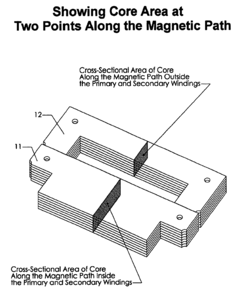
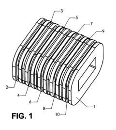
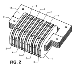
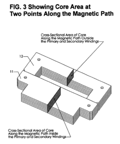
Method for increased coupling coefficient in a pulse type transformer through coil configuration and varied core area
PatentInactiveUS6822549B2
Innovation
- A coreless pulse type transformer with multiple primary and secondary windings arranged in close proximity and a magnetic pulse type transformer with varying cross-sectional area along the magnetic path, both designed to increase the coupling coefficient by optimizing the physical arrangement and core design.
Materials Science Considerations for Composite Nanostructures
The selection of materials for composite nanostructures is critical for enhancing coupling coefficients. Material properties such as permittivity, permeability, conductivity, and thermal stability directly influence the electromagnetic interactions at the nanoscale. When designing composite nanostructures, the interface between different materials becomes a crucial consideration, as it often determines the quality of coupling and energy transfer efficiency.
Noble metals like gold and silver exhibit excellent plasmonic properties, making them ideal candidates for coupling enhancement. Their ability to support surface plasmon resonances at optical frequencies enables strong field localization and enhancement. However, these metals suffer from high ohmic losses, which can diminish coupling efficiency at certain frequencies. Incorporating dielectric materials with high refractive indices, such as silicon or titanium dioxide, can mitigate these losses while maintaining strong field confinement.
Metamaterials and metasurfaces offer another promising avenue for coupling enhancement. By engineering artificial structures with subwavelength dimensions, researchers can create materials with extraordinary electromagnetic properties not found in nature. These include negative refractive indices, epsilon-near-zero behavior, and hyperbolic dispersion, all of which can significantly boost coupling coefficients when properly designed.
The crystalline structure and orientation of materials also play vital roles in coupling performance. Single-crystal structures typically exhibit superior coupling characteristics compared to polycrystalline or amorphous counterparts due to reduced scattering and defect-related losses. Furthermore, the crystallographic orientation can be exploited to leverage anisotropic properties, enabling directional coupling enhancement.
Nanofabrication techniques must be carefully selected based on material compatibility and desired structural precision. Methods such as atomic layer deposition offer excellent conformality and thickness control, while self-assembly approaches can create complex hierarchical structures with unique coupling properties. The choice of fabrication technique often imposes constraints on material selection and vice versa.
Temperature stability represents another critical consideration, particularly for applications involving high power densities or extreme environmental conditions. Materials with mismatched thermal expansion coefficients may experience stress-induced deformation or delamination, compromising coupling performance over time. Ceramic-based composites often provide superior thermal stability compared to polymer-based alternatives.
Recent advances in two-dimensional materials like graphene, transition metal dichalcogenides, and hexagonal boron nitride have opened new possibilities for coupling enhancement. These atomically thin materials exhibit exceptional optical and electronic properties that can be leveraged to create ultrathin, highly efficient coupling structures when combined with traditional materials in van der Waals heterostructures.
Scalability and Manufacturing Challenges for Practical Implementation
The transition from laboratory-scale demonstrations to commercial-scale production of composite nanostructures for enhanced coupling coefficients faces significant manufacturing challenges. Current fabrication methods such as chemical vapor deposition, atomic layer deposition, and molecular beam epitaxy provide excellent control over nanostructure formation but are inherently limited in throughput and scalability. These techniques typically process small surface areas and require precise environmental controls, making them prohibitively expensive for mass production.
Material consistency represents another critical challenge. Maintaining uniform properties across large batches of composite nanostructures is difficult due to the sensitivity of nanoscale features to minor variations in processing conditions. Even slight deviations in temperature, pressure, or precursor concentrations can lead to significant performance inconsistencies, directly affecting the coupling coefficient enhancement capabilities of the final product.
Cost considerations further complicate commercial implementation. The specialized equipment, ultra-pure materials, and controlled environments necessary for fabricating high-quality composite nanostructures contribute to high production costs. Current estimates suggest that manufacturing costs must decrease by at least an order of magnitude to make these technologies commercially viable for widespread applications beyond specialized high-value sectors.
Integration challenges also present significant hurdles. Incorporating these nanostructures into existing manufacturing processes and products requires developing compatible integration methods that preserve the enhanced coupling properties while maintaining structural integrity. The interface between the nanostructured components and conventional materials often becomes a performance bottleneck, requiring careful engineering to minimize coupling losses.
Environmental and safety concerns associated with nanomaterial production and handling add another layer of complexity. Regulatory frameworks for nanomaterials continue to evolve, potentially imposing additional compliance requirements that may impact manufacturing processes and costs. Addressing potential health and environmental risks requires implementing appropriate containment and waste management systems.
Recent advances in roll-to-roll processing, solution-based synthesis methods, and directed self-assembly techniques show promise for overcoming some scalability limitations. These approaches could potentially reduce production costs while maintaining adequate control over nanostructure formation. However, significant research and development efforts are still needed to achieve the precision and reliability required for coupling coefficient enhancement applications at industrial scales.
Unlock deeper insights with Patsnap Eureka Quick Research — get a full tech report to explore trends and direct your research. Try now!
Generate Your Research Report Instantly with AI Agent
Supercharge your innovation with Patsnap Eureka AI Agent Platform!