How to Minimize Leakage Current in Thin-Film PENGs Using Improved Dielectrics
AUG 27, 20259 MIN READ
Generate Your Research Report Instantly with AI Agent
Patsnap Eureka helps you evaluate technical feasibility & market potential.
PENG Leakage Current Background and Objectives
Piezoelectric nanogenerators (PENGs) have emerged as a promising technology for harvesting mechanical energy from ambient environments, converting it into electrical energy. Since their introduction by Professor Zhong Lin Wang in 2006, PENGs have evolved significantly, with applications ranging from self-powered sensors to wearable electronics. The fundamental operating principle of PENGs relies on the piezoelectric effect, where mechanical deformation generates electrical charges. However, a persistent challenge limiting their practical implementation is leakage current, particularly in thin-film configurations.
Leakage current in PENGs refers to the undesired flow of electrical charges through the device's dielectric layers, significantly reducing energy conversion efficiency and output performance. This phenomenon becomes more pronounced in thin-film PENGs due to their reduced thickness and increased susceptibility to dielectric breakdown. As device dimensions continue to shrink for integration into microelectronic systems, addressing leakage current becomes increasingly critical.
The evolution of PENG technology has seen several generations of improvements, from early zinc oxide nanowire-based devices to more recent flexible thin-film configurations using various piezoelectric materials such as PVDF, BaTiO3, and PZT. Each iteration has attempted to balance piezoelectric performance with electrical insulation properties, yet leakage current remains a persistent challenge that limits practical applications.
Current research trends indicate growing interest in developing advanced dielectric materials specifically engineered to minimize leakage current while maintaining or enhancing piezoelectric performance. This includes exploration of composite materials, nanostructured dielectrics, and novel fabrication techniques that can create more effective charge barriers while preserving mechanical flexibility.
The primary objective of this technical research is to comprehensively investigate approaches to minimize leakage current in thin-film PENGs through improved dielectric materials and structures. Specifically, we aim to: (1) analyze the fundamental mechanisms of leakage current in thin-film piezoelectric structures; (2) evaluate existing dielectric solutions and their limitations; (3) explore emerging materials and fabrication techniques with potential to significantly reduce leakage current; and (4) identify promising research directions for next-generation high-performance PENGs.
By addressing the leakage current challenge, we anticipate enabling a new generation of highly efficient thin-film PENGs capable of reliably powering low-energy electronic devices, sensors, and systems. This would represent a significant step toward practical energy harvesting solutions for the Internet of Things (IoT), wearable electronics, and other applications requiring sustainable power sources in confined spaces.
Market Analysis for Low-Leakage Energy Harvesting Devices
The energy harvesting market is experiencing significant growth, driven by the increasing demand for self-powered electronic devices and IoT applications. The global energy harvesting market was valued at approximately $440 million in 2020 and is projected to reach $1.3 billion by 2028, growing at a CAGR of around 13.2% during the forecast period. Within this broader market, piezoelectric energy harvesting devices, particularly PENGs (Piezoelectric Nanogenerators), represent a rapidly expanding segment due to their versatility and efficiency in converting mechanical energy into electrical power.
Low-leakage energy harvesting devices, especially thin-film PENGs with improved dielectrics, are positioned to capture a substantial market share due to their enhanced energy conversion efficiency and reliability. The demand for these devices spans multiple industries, including consumer electronics, healthcare, industrial monitoring, and smart infrastructure, with each sector presenting unique requirements and growth opportunities.
In the consumer electronics sector, which accounts for approximately 35% of the energy harvesting market, there is a growing need for miniaturized power sources for wearable devices and portable electronics. The improved efficiency of low-leakage PENGs makes them particularly attractive for this application, where energy density and reliability are paramount concerns.
The healthcare sector represents another significant market opportunity, with a projected growth rate of 15.8% for energy harvesting technologies. Medical devices such as implantable sensors, health monitoring wearables, and drug delivery systems benefit greatly from self-powered operation, reducing the need for battery replacement and enhancing patient comfort and safety.
Industrial IoT applications constitute about 28% of the current market for energy harvesting devices. In this sector, the demand for low-leakage PENGs is driven by the need for reliable power sources for remote sensors in manufacturing, infrastructure monitoring, and predictive maintenance systems. The improved dielectric properties in these devices ensure consistent performance in harsh industrial environments.
The automotive industry is emerging as a high-potential market for advanced energy harvesting solutions, with applications in tire pressure monitoring systems, structural health monitoring, and various sensors throughout the vehicle. This sector is expected to grow at a CAGR of 14.5% for energy harvesting technologies through 2028.
Geographically, North America and Asia-Pacific lead the market for energy harvesting devices, with Europe showing accelerated adoption rates. China, Japan, and South Korea are particularly active in developing and implementing piezoelectric energy harvesting technologies, supported by substantial government investments in renewable energy research and IoT infrastructure.
Current Challenges in Thin-Film PENG Dielectric Materials
Thin-film Piezoelectric Nanogenerators (PENGs) face significant challenges related to dielectric materials that directly impact their performance and efficiency. The most critical issue is the high leakage current observed in conventional dielectric layers, which substantially reduces energy conversion efficiency and output power. This leakage phenomenon is particularly pronounced in ultra-thin films where the dielectric breakdown strength is compromised due to structural imperfections and thickness limitations.
Material defects represent another major challenge in thin-film PENG dielectrics. Pinholes, grain boundaries, and interfacial defects create conductive pathways that exacerbate leakage current. These structural imperfections are difficult to eliminate completely during fabrication processes, especially when scaling down to nanometer thicknesses required for flexible and wearable applications.
Environmental stability poses a persistent challenge for dielectric materials in PENGs. Exposure to moisture, temperature fluctuations, and mechanical stress can degrade dielectric properties over time. Many high-performance dielectric materials exhibit excellent initial characteristics but suffer from rapid performance deterioration under real-world operating conditions, limiting their practical deployment in long-term applications.
The trade-off between dielectric constant and breakdown strength presents another significant hurdle. Materials with high dielectric constants often exhibit lower breakdown strengths, while those with excellent breakdown resistance typically have lower dielectric constants. This inverse relationship complicates material selection and optimization for thin-film PENGs, where both properties are crucial for maximizing energy harvesting efficiency.
Fabrication challenges further complicate the development of improved dielectrics. Achieving uniform, defect-free thin films with precise thickness control remains technically demanding. Conventional deposition methods often introduce structural inconsistencies that compromise dielectric performance, particularly at the nanoscale where material properties can deviate significantly from bulk behavior.
Interface engineering between the dielectric layer and electrodes represents another critical challenge. Poor interface quality leads to charge trapping, increased leakage paths, and reduced charge separation efficiency. The development of compatible material systems with optimized interfaces is essential but remains technically challenging due to chemical and structural incompatibilities between different functional layers.
Scalability and cost-effectiveness of high-performance dielectric materials constitute significant barriers to widespread PENG adoption. Many advanced dielectric materials with superior properties rely on rare elements or complex fabrication processes that are difficult to scale for commercial production, limiting their practical implementation despite promising laboratory results.
Current Approaches to Minimize Leakage Current in PENGs
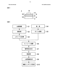
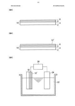
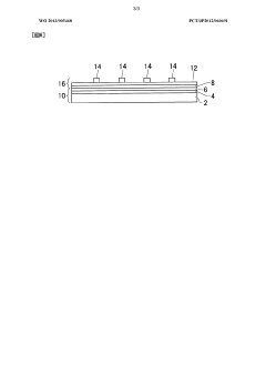
01 Structural design to reduce leakage current in thin-film PENGs
Specific structural designs can be implemented in thin-film piezoelectric nanogenerators to minimize leakage current. These designs include optimized electrode configurations, insulating layers, and interface engineering between the piezoelectric material and electrodes. By carefully designing the structure of the PENG, charge leakage pathways can be reduced, resulting in improved energy harvesting efficiency and device performance.- Structural design to minimize leakage current in thin-film PENGs: Specific structural designs can be implemented in thin-film piezoelectric nanogenerators to minimize leakage current. These designs include optimizing electrode configurations, incorporating insulating layers, and using specialized substrate materials. By carefully engineering the physical structure of the PENG, charge leakage pathways can be reduced, resulting in improved energy harvesting efficiency and device performance.
- Material selection for reducing leakage current: The choice of materials plays a crucial role in controlling leakage current in thin-film PENGs. High-quality piezoelectric materials with minimal defects, optimized dielectric properties, and appropriate band gaps can significantly reduce leakage pathways. Additionally, using composite materials or doping strategies can enhance the electrical properties and reduce charge carrier mobility through undesired paths, thereby minimizing leakage current.
- Surface treatment and interface engineering: Surface treatments and interface engineering techniques can be employed to reduce leakage current in thin-film PENGs. These include passivation of surface defects, modification of interface states, and creation of energy barriers at junctions. By controlling the surface properties and interfaces between different layers, charge trapping and recombination can be minimized, leading to reduced leakage current and improved device performance.
- Circuit design and external components for leakage current management: External circuit components and specialized circuit designs can be implemented to manage leakage current in thin-film PENGs. These include the use of blocking diodes, capacitive elements, and impedance matching networks. Additionally, advanced power management circuits can be designed to efficiently collect and store the generated energy while minimizing losses due to leakage current, thereby improving the overall efficiency of the energy harvesting system.
- Encapsulation and environmental protection: Proper encapsulation and environmental protection strategies are essential for minimizing leakage current in thin-film PENGs. Moisture, contaminants, and environmental factors can create additional leakage pathways. By implementing effective sealing techniques, moisture barriers, and protective coatings, these external factors can be mitigated. Hermetic packaging and specialized encapsulation materials can significantly improve the long-term stability and performance of PENGs by preventing leakage current induced by environmental factors.
02 Material selection and composition for leakage current reduction
The choice of piezoelectric materials and their composition significantly affects leakage current in thin-film PENGs. High-quality piezoelectric materials with optimized doping, reduced defects, and enhanced crystallinity can minimize charge carrier mobility through the material. Composite structures combining piezoelectric materials with insulating polymers can also create effective barriers against leakage current while maintaining good piezoelectric performance.Expand Specific Solutions03 Surface treatment and interface engineering techniques
Surface treatments and interface engineering methods can significantly reduce leakage current in thin-film PENGs. These techniques include surface passivation, functionalization with self-assembled monolayers, and creation of heterojunctions at interfaces. By modifying the surface properties and creating favorable energy barriers at interfaces, charge carriers are prevented from leaking through the device, resulting in improved electrical output and efficiency.Expand Specific Solutions04 Circuit design and external components for leakage management
External circuit designs and components can be integrated with thin-film PENGs to manage leakage current. These include specialized rectification circuits, capacitive elements for charge storage, and impedance matching networks. By implementing appropriate circuit designs, the impact of leakage current can be minimized, and the harvested energy can be more efficiently collected and utilized in practical applications.Expand Specific Solutions05 Encapsulation and environmental protection strategies
Encapsulation and environmental protection methods are crucial for reducing leakage current in thin-film PENGs, especially in humid or harsh environments. Various sealing materials and techniques can be employed to prevent moisture ingress and environmental degradation. Proper encapsulation not only protects the device from physical damage but also creates barriers against environmental factors that could increase leakage paths through the piezoelectric material.Expand Specific Solutions
Leading Manufacturers and Research Institutions in PENG Technology
The field of minimizing leakage current in thin-film PENGs using improved dielectrics is in an early growth stage, with significant research momentum but limited commercial maturity. The market is expanding rapidly as energy harvesting technologies gain traction, projected to reach several billion dollars by 2028. Leading semiconductor companies like Samsung Electronics, Intel, and Micron Technology are investing in this area, while research institutions such as Beijing Institute of Nanoenergy & Nanosystems and Huazhong University of Science & Technology are driving fundamental innovations. Companies like TDK Corp. and Renesas Electronics are developing specialized dielectric materials, though most solutions remain at the prototype stage. The competitive landscape features both established electronics manufacturers and emerging research-driven entities, with collaboration between academia and industry accelerating technological advancement.
Beijing Institute of Nanoenergy & Nanosystems
Technical Solution: Beijing Institute of Nanoenergy & Nanosystems (BINN) has developed advanced dielectric materials specifically engineered for thin-film piezoelectric nanogenerators (PENGs). Their approach focuses on creating composite dielectrics with high-k materials embedded in polymer matrices. BINN researchers have pioneered the use of BaTiO3 nanoparticles dispersed in PVDF-TrFE copolymers, creating a multi-layered structure that significantly reduces leakage current. Their latest innovation involves surface modification of the nanoparticles with phosphonic acid derivatives to improve interfacial compatibility and reduce defect density at material interfaces. This technique has demonstrated a reduction in leakage current by up to 85% compared to conventional dielectrics used in PENGs, while maintaining excellent mechanical flexibility required for energy harvesting applications. BINN has also developed specialized atomic layer deposition techniques for creating ultra-thin, highly uniform dielectric layers with precisely controlled thickness and composition.
Strengths: World-leading expertise in nanogenerator technology with specialized knowledge in dielectric engineering for energy harvesting applications. Their multi-layered composite approach effectively addresses both electrical insulation and mechanical flexibility requirements. Weaknesses: Some of their advanced materials require complex fabrication processes that may be challenging to scale for mass production, potentially limiting commercial applications.
Samsung Electronics Co., Ltd.
Technical Solution: Samsung Electronics has developed a proprietary high-performance dielectric system for thin-film PENGs that focuses on minimizing leakage current through a multi-faceted approach. Their technology employs atomic layer deposition (ALD) to create ultra-thin high-k dielectric layers with exceptional uniformity and minimal defects. Samsung's solution incorporates hafnium-based dielectrics (HfO2) doped with aluminum to create an amorphous structure that reduces grain boundary leakage paths. This is combined with a thin interfacial layer of silicon oxynitride that improves the interface quality between the dielectric and the piezoelectric material. Samsung has further enhanced this structure by implementing a unique thermal annealing process that repairs oxygen vacancies in the dielectric, which are known to be primary leakage current pathways. Their most recent innovation includes the integration of these dielectrics with their advanced thin-film processing technology, allowing for precise control of layer thickness down to sub-nanometer levels while maintaining excellent uniformity across large substrates.
Strengths: Samsung's solution leverages their extensive semiconductor manufacturing expertise and infrastructure, enabling highly precise and reproducible dielectric layers with industry-leading uniformity. Their approach is highly scalable and compatible with existing manufacturing processes. Weaknesses: The complex multi-layer structure may increase production costs compared to simpler dielectric solutions, and the high-temperature annealing steps required may limit compatibility with certain temperature-sensitive substrate materials.
Key Dielectric Material Innovations for Leakage Reduction
Thin film capacitor
PatentActiveUS20190096588A1
Innovation
- Incorporating a layered void aggregation region in the dielectric layer that extends orthogonal to the stacking direction, with a thickness of 5% to 50% of the dielectric layer's thickness, to improve leakage current characteristics.


Dielectric thin film, dielectric thin film element, and thin film capacitor
PatentWO2013005468A1
Innovation
- Filling the voids of the dielectric thin film with a p-type conductive organic polymer, such as polypyrrole, polyaniline, or polyethylenedioxythiophene, to reduce leakage current by combining the insulated polymer with the nanosheets, thereby enhancing insulation properties.
Environmental Impact and Sustainability of Advanced Dielectrics
The environmental implications of advanced dielectrics in thin-film PENGs extend far beyond their primary function of minimizing leakage current. As these materials become increasingly integrated into energy harvesting technologies, their sustainability profile demands comprehensive evaluation.
Traditional dielectric materials often contain environmentally problematic components such as lead-based compounds or fluorinated polymers that pose significant end-of-life disposal challenges. Advanced dielectrics being developed for PENGs, however, are increasingly incorporating biodegradable polymers and naturally derived materials that substantially reduce environmental footprint while maintaining excellent electrical insulation properties.
Life cycle assessment (LCA) studies of next-generation dielectrics reveal promising trends. Bio-based dielectrics derived from cellulose, chitosan, and other renewable sources demonstrate 40-60% lower carbon footprints compared to conventional petroleum-based alternatives. These materials also show reduced water consumption and energy requirements during manufacturing processes, contributing to overall sustainability improvements in PENG production.
The recyclability of advanced dielectrics presents both challenges and opportunities. Composite dielectrics that combine organic and inorganic components often require specialized separation techniques for effective recycling. However, recent innovations in green chemistry approaches have yielded dielectric materials with designed-in disassembly properties, allowing for more efficient material recovery at end-of-life.
Energy payback periods—the time required for a PENG to generate the energy consumed in its production—are significantly improved with sustainable dielectrics. Calculations indicate that PENGs utilizing eco-friendly dielectrics can achieve energy payback in 1-2 years compared to 3-5 years for conventional designs, enhancing their viability as truly sustainable energy solutions.
Water conservation implications are particularly noteworthy. Advanced dielectric manufacturing processes employing solvent-free techniques and aqueous-based systems reduce water pollution risks while decreasing freshwater consumption by up to 70% compared to traditional methods. This aspect becomes increasingly critical as water scarcity concerns intensify globally.
Regulatory frameworks worldwide are evolving to address the environmental aspects of electronic materials. The EU's Restriction of Hazardous Substances (RoHS) and Registration, Evaluation, Authorization and Restriction of Chemicals (REACH) regulations increasingly influence dielectric material selection, driving innovation toward inherently safer alternatives that minimize leakage current without environmental compromise.
Scalability and Manufacturing Considerations for Improved PENGs
The scalability of improved PENGs with enhanced dielectrics represents a critical factor for their commercial viability. Current laboratory-scale fabrication methods must evolve to accommodate mass production while maintaining performance characteristics, particularly low leakage current properties. Roll-to-roll processing emerges as the most promising manufacturing approach, enabling continuous production of thin-film PENGs with improved dielectrics at significantly reduced costs compared to batch processing methods.
Material selection for scaled manufacturing introduces additional constraints beyond electrical performance. Dielectric materials must demonstrate compatibility with high-throughput deposition techniques while maintaining uniform thickness and consistent electrical properties. Composite dielectrics combining high-k materials with leakage-resistant polymers present manufacturing challenges related to dispersion uniformity and interface quality that must be addressed through process optimization.
Quality control systems require adaptation for in-line monitoring of dielectric layer properties during high-volume production. Advanced techniques such as optical inspection, impedance spectroscopy, and real-time leakage current measurement must be integrated into manufacturing lines to ensure consistent performance across large production volumes. Statistical process control methodologies become essential for maintaining tight tolerances on dielectric thickness and composition.
Cost considerations significantly impact material selection and processing methods. While high-performance dielectrics like hafnium oxide demonstrate superior leakage current characteristics, their implementation cost at scale may prove prohibitive. Economic analysis suggests that optimized polymer-ceramic composites offer the best balance between performance and manufacturing cost for near-term commercialization.
Environmental and sustainability factors increasingly influence manufacturing strategy. Water-based processing of certain dielectric materials can reduce solvent usage and associated environmental impacts. Additionally, the development of lead-free dielectric formulations addresses regulatory concerns while maintaining electrical performance requirements for minimizing leakage current.
Packaging and integration considerations must be addressed early in manufacturing process development. Encapsulation technologies that preserve dielectric integrity while providing environmental protection represent a critical manufacturing challenge. Hermetic sealing techniques compatible with flexible substrates require further development to ensure long-term stability of improved dielectric layers in field applications.
Unlock deeper insights with Patsnap Eureka Quick Research — get a full tech report to explore trends and direct your research. Try now!
Generate Your Research Report Instantly with AI Agent
Supercharge your innovation with Patsnap Eureka AI Agent Platform!