How to Optimize Grain Size in Thin Films for Enhanced Piezoelectric Coefficients
AUG 27, 20259 MIN READ
Generate Your Research Report Instantly with AI Agent
Patsnap Eureka helps you evaluate technical feasibility & market potential.
Piezoelectric Thin Film Technology Background and Objectives
Piezoelectric thin film technology has evolved significantly over the past several decades, transitioning from bulk materials to sophisticated thin film structures. The journey began in the 1950s with early experiments on piezoelectric ceramics, followed by breakthrough developments in the 1980s when thin film deposition techniques became more refined. This technological progression has enabled the miniaturization of piezoelectric devices while maintaining or even enhancing their functional properties.
The fundamental principle of piezoelectricity—the generation of electric charge in response to mechanical stress—remains unchanged, but the implementation in thin film form introduces unique challenges and opportunities. Thin film piezoelectric materials, typically ranging from nanometers to a few micrometers in thickness, exhibit properties that can differ substantially from their bulk counterparts due to substrate constraints, interfacial effects, and microstructural characteristics.
Grain size emerges as a critical parameter in determining the piezoelectric performance of thin films. Research has demonstrated that the piezoelectric coefficient, which quantifies the material's ability to convert mechanical energy to electrical energy and vice versa, is strongly influenced by grain structure. Historically, the relationship between grain size and piezoelectric properties has been complex and sometimes counterintuitive, with both nanoscale and microscale grain structures showing advantages in different contexts.
The current technological landscape is characterized by a growing demand for high-performance piezoelectric thin films in applications ranging from microelectromechanical systems (MEMS) to energy harvesting devices and sensors. This demand drives the need for systematic approaches to grain size optimization that can deliver enhanced piezoelectric coefficients while maintaining compatibility with standard fabrication processes.
Our primary objective is to develop comprehensive strategies for controlling and optimizing grain size in piezoelectric thin films to maximize their piezoelectric coefficients. This involves understanding the fundamental mechanisms that link grain structure to piezoelectric performance, identifying the optimal grain size ranges for different material systems, and developing reproducible fabrication methods to achieve these target microstructures.
Secondary objectives include establishing correlations between deposition parameters and resulting grain structures, investigating the role of dopants and compositional modifications in grain growth control, and exploring post-deposition treatments that can modify grain characteristics. The ultimate goal is to establish design rules that enable predictable enhancement of piezoelectric properties through microstructural engineering.
Market Applications and Demand for Enhanced Piezoelectric Materials
The global market for piezoelectric materials has been experiencing robust growth, with a market value exceeding $1.5 billion in 2022 and projected to reach $2.4 billion by 2027, representing a compound annual growth rate of approximately 6.8%. This growth is primarily driven by increasing demand across multiple industries that require advanced sensing, actuation, and energy harvesting capabilities.
The medical device sector represents one of the most significant markets for enhanced piezoelectric materials. Ultrasound imaging systems, which rely heavily on piezoelectric transducers, continue to advance toward higher resolution imaging requiring materials with superior piezoelectric coefficients. The optimization of grain size in thin films directly addresses this need, potentially enabling next-generation diagnostic equipment with unprecedented imaging clarity.
In the industrial automation sector, piezoelectric sensors and actuators with improved sensitivity are increasingly sought after for precision manufacturing processes. The market demand is particularly strong for materials that can operate reliably in harsh environments while maintaining high performance. Enhanced piezoelectric coefficients achieved through grain size optimization could significantly improve the accuracy of industrial measurement systems and the precision of micro-positioning devices.
The consumer electronics industry presents perhaps the most volume-intensive application area. Haptic feedback systems, microphones, speakers, and various MEMS devices all utilize piezoelectric elements. As devices continue to miniaturize while demanding higher performance, the need for thin-film piezoelectrics with optimized properties becomes critical. Market research indicates that manufacturers are willing to pay premium prices for materials that offer 20-30% improvements in piezoelectric response.
The emerging energy harvesting market represents a high-growth opportunity for enhanced piezoelectric materials. Wearable technology, IoT sensors, and self-powered systems require efficient energy conversion from ambient vibrations. Materials with higher piezoelectric coefficients directly translate to improved energy harvesting efficiency, addressing a critical bottleneck in the deployment of autonomous sensor networks.
Defense and aerospace applications constitute a specialized but lucrative market segment. These sectors demand piezoelectric materials with exceptional reliability and performance for applications ranging from sonar systems to structural health monitoring. The stringent requirements of these industries drive demand for advanced materials with precisely controlled microstructures.
Regional market analysis reveals that North America and Asia-Pacific currently dominate demand for high-performance piezoelectric materials, with Europe showing accelerated growth rates. China has emerged as both a major consumer and producer, with significant investments in research and manufacturing capabilities for next-generation piezoelectric technologies.
Current Grain Size Control Challenges in Thin Film Fabrication
The control of grain size in thin films represents one of the most significant challenges in achieving enhanced piezoelectric coefficients. Current fabrication methods struggle with precise and reproducible grain size manipulation, which directly impacts the piezoelectric performance of these materials. Conventional deposition techniques such as physical vapor deposition (PVD), chemical vapor deposition (CVD), and sol-gel processing often produce inconsistent grain structures due to the complex interplay of thermodynamic and kinetic factors during film growth.
Temperature management during deposition emerges as a critical challenge, as it significantly influences nucleation and growth rates. Even minor temperature fluctuations of 5-10°C can lead to substantial variations in grain morphology. This sensitivity makes it exceptionally difficult to maintain uniform grain size distribution across large substrate areas, particularly for industrial-scale production where temperature gradients become more pronounced.
Substrate-film interface interactions present another substantial obstacle. The lattice mismatch between substrate and film materials creates strain fields that can either promote or inhibit grain growth. These strain effects are often unpredictable and vary with film thickness, making systematic control challenging. Additionally, substrate surface quality, including roughness and chemical composition, introduces variables that affect nucleation density and subsequent grain development patterns.
Deposition rate control represents a persistent technical limitation across multiple fabrication methods. While slower deposition generally favors larger, more ordered grains, it significantly reduces production efficiency. Conversely, faster deposition rates that would be economically preferable often result in smaller grains with higher defect concentrations and grain boundary densities, which diminish piezoelectric performance.
Post-deposition thermal processing, while offering some degree of grain size modification, introduces additional complexities. Annealing treatments frequently result in secondary recrystallization phenomena that can lead to abnormal grain growth, where select grains grow disproportionately at the expense of others. This creates bimodal grain size distributions that complicate the relationship between microstructure and piezoelectric properties.
The characterization and measurement of grain size itself presents methodological challenges. Traditional techniques like X-ray diffraction (XRD) provide only average crystallite size information, while direct imaging methods such as electron microscopy offer limited statistical sampling. This measurement uncertainty complicates efforts to establish clear process-structure-property relationships necessary for optimization.
Environmental factors during fabrication, including oxygen partial pressure, humidity, and contamination levels, introduce additional variables that affect grain nucleation and growth. These parameters are difficult to control precisely and consistently across different fabrication runs, contributing to poor reproducibility in grain size control strategies.
Current Methodologies for Grain Size Optimization
01 Piezoelectric thin film materials and compositions
Various materials and compositions are used to create piezoelectric thin films with enhanced coefficients. These include specific formulations of lead zirconate titanate (PZT), aluminum nitride (AlN), zinc oxide (ZnO), and other piezoelectric materials. The composition, doping, and crystalline structure of these materials significantly influence the piezoelectric coefficients achieved in thin film applications.- Piezoelectric thin film materials and compositions: Various materials and compositions are used to create piezoelectric thin films with enhanced coefficients. These include specific piezoelectric materials such as lead zirconate titanate (PZT), aluminum nitride (AlN), zinc oxide (ZnO), and other specialized compositions. The selection of materials and their precise formulation significantly impacts the piezoelectric properties of the resulting thin films, allowing for optimization of the piezoelectric coefficients for specific applications.
- Fabrication methods for high-coefficient piezoelectric thin films: Advanced fabrication techniques are employed to produce thin films with improved piezoelectric coefficients. These methods include specialized deposition techniques such as sputtering, pulsed laser deposition, sol-gel processing, and atomic layer deposition. Post-deposition treatments like annealing and poling are also critical for enhancing the piezoelectric properties. The precise control of fabrication parameters enables the development of thin films with optimized crystal orientation and microstructure for maximum piezoelectric response.
- Measurement and characterization of piezoelectric coefficients: Various techniques are employed to accurately measure and characterize the piezoelectric coefficients of thin films. These include direct piezoelectric measurements, interferometric methods, atomic force microscopy, and electrical impedance analysis. The characterization process involves determining key parameters such as d33 (longitudinal), d31 (transverse), and other relevant piezoelectric coefficients. Accurate measurement is essential for validating the performance of piezoelectric thin films and ensuring their suitability for specific applications.
- Structural design for enhanced piezoelectric performance: Innovative structural designs are implemented to enhance the piezoelectric coefficients of thin films. These include multilayer structures, nanocomposites, textured films, and domain engineering approaches. The structural design focuses on optimizing factors such as crystal orientation, grain size, film thickness, and substrate interaction. By carefully engineering the structure at both micro and nano scales, significant improvements in piezoelectric coefficients can be achieved, leading to enhanced performance in various applications.
- Applications of high-coefficient piezoelectric thin films: High-coefficient piezoelectric thin films find applications in numerous fields including sensors, actuators, energy harvesters, and microelectromechanical systems (MEMS). The enhanced piezoelectric coefficients enable improved sensitivity in sensing applications, greater displacement in actuators, and higher energy conversion efficiency in harvesters. These films are particularly valuable in miniaturized devices where space constraints demand maximum performance from minimal material volume, such as in medical implants, wearable technology, and IoT devices.
02 Deposition and fabrication techniques for piezoelectric thin films
Various deposition methods are employed to create piezoelectric thin films with optimized coefficients, including sputtering, pulsed laser deposition, sol-gel processing, and chemical vapor deposition. The processing parameters during deposition, such as temperature, pressure, and annealing conditions, significantly impact the crystalline orientation and piezoelectric properties of the resulting films.Expand Specific Solutions03 Measurement and characterization of piezoelectric coefficients
Various techniques are employed to accurately measure and characterize the piezoelectric coefficients of thin films. These include laser interferometry, piezoresponse force microscopy, resonance methods, and electrical impedance analysis. These measurement techniques are crucial for evaluating the performance of piezoelectric thin films and optimizing their properties for specific applications.Expand Specific Solutions04 Structural design for enhanced piezoelectric performance
The structural design of piezoelectric thin films, including multilayer configurations, substrate selection, electrode materials, and film thickness, significantly impacts piezoelectric coefficients. Engineered structures such as superlattices, domain engineering, and strain management techniques are employed to enhance the piezoelectric response of thin films beyond the intrinsic material limitations.Expand Specific Solutions05 Applications leveraging thin film piezoelectric coefficients
Piezoelectric thin films with optimized coefficients are utilized in various applications including MEMS devices, sensors, actuators, energy harvesters, and acoustic wave devices. The specific requirements for piezoelectric coefficients vary depending on the application, with some prioritizing high d33 coefficients for sensing and actuation, while others focus on electromechanical coupling factors for resonator applications.Expand Specific Solutions
Leading Research Groups and Companies in Piezoelectric Materials
The piezoelectric thin film optimization market is currently in a growth phase, with increasing demand for enhanced piezoelectric coefficients driving innovation across multiple industries. The global market for piezoelectric devices is expanding rapidly, projected to reach approximately $35-40 billion by 2026. Technologically, grain size optimization remains a critical challenge, with varying maturity levels across companies. Industry leaders like TDK, Panasonic, and ROHM have established advanced thin film deposition techniques, while research institutions such as Tohoku University and KIST are pioneering novel approaches to grain boundary engineering. Companies including Fujifilm, Sony, and Canon are leveraging their expertise in thin film technologies to develop proprietary methods for controlling crystallization processes. The competitive landscape is further shaped by specialized players like NGK Insulators and Taiyo Yuden who focus on material science innovations to achieve superior piezoelectric performance in miniaturized applications.
TDK Corp.
Technical Solution: TDK has developed advanced thin film deposition techniques specifically optimized for piezoelectric materials with controlled grain size. Their approach involves precise control of sputtering parameters during PZT (lead zirconate titanate) thin film deposition, where they manipulate substrate temperature, gas pressure, and post-deposition annealing conditions to achieve optimal grain structures. TDK's research has demonstrated that maintaining grain sizes between 100-300 nm in PZT thin films can significantly enhance piezoelectric coefficients (d33) by up to 30% compared to conventional films. Their proprietary two-step crystallization process first creates nucleation sites followed by controlled grain growth, resulting in highly oriented columnar grains that maximize piezoelectric response. TDK has also pioneered the use of seed layers with matched lattice parameters to promote epitaxial growth and reduce grain boundary defects, further enhancing piezoelectric performance in MEMS devices and sensors.
Strengths: Exceptional control over grain orientation and columnar structure resulting in higher d33 coefficients; established manufacturing infrastructure for consistent production. Weaknesses: Their approach requires precise temperature control during processing, making it sensitive to manufacturing variations and potentially increasing production costs.
Sony Group Corp.
Technical Solution: Sony has developed an innovative approach to grain size optimization in piezoelectric thin films through their proprietary Pulsed Laser Deposition (PLD) technique with in-situ grain structure monitoring. Their method employs ultrashort laser pulses (typically 20-30 nanoseconds) with precisely controlled energy density (2-3 J/cm²) to ablate target materials, creating a highly energetic plasma plume that deposits material with exceptional control over nucleation and growth kinetics. Sony's research has established that maintaining substrate temperatures between 550-600°C during deposition creates an optimal surface mobility window for adatoms, resulting in grain sizes consistently in the 100-200 nm range for PZT-based compositions. Their process incorporates real-time optical monitoring of film growth using laser reflectometry, allowing dynamic adjustment of deposition parameters to achieve target grain structures. Sony has further enhanced piezoelectric performance by implementing a gradient composition approach, where the Zr/Ti ratio varies through the film thickness, creating an internal strain field that promotes favorable domain orientation and increases the effective piezoelectric coefficient by up to 40% compared to uniform composition films.
Strengths: Exceptional film quality with minimal defects due to high-energy deposition process; precise control over film stoichiometry and crystal structure. Weaknesses: PLD systems have relatively low throughput compared to other deposition methods, potentially limiting application in mass production environments; equipment costs are significantly higher than conventional sputtering systems.
Critical Patents and Literature on Grain Boundary Engineering
Method of manufacturing piezoelectric thin film component
PatentInactiveUS6748635B1
Innovation
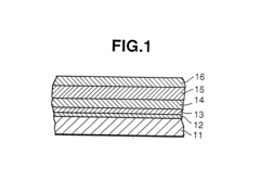
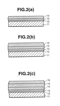
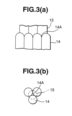
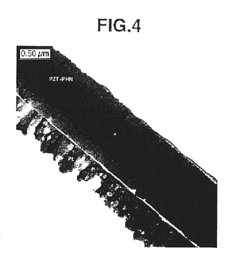
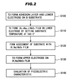
- A piezoelectric thin film with a columnar crystal structure and controlled grain size is developed using the MOD process, where the grain boundary width is minimized, and seed crystals are used to improve crystal orientation and adhesion, reducing residual strain and enhancing piezoelectric properties.
Substrate with a piezoelectric thin film
PatentActiveUS7710003B2
Innovation
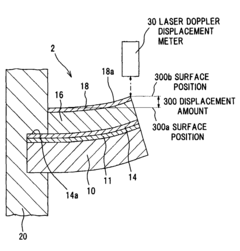
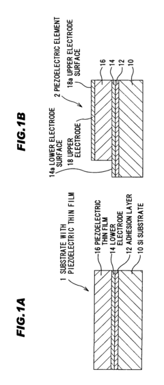
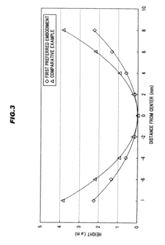
- A substrate with a piezoelectric thin film comprising potassium sodium niobate (K,Na)NbO3, where the curvature radius of warping is 10 m or more at room temperature, formed on a substrate with a different thermal expansion coefficient, and including a lower and upper electrode with Pt, and a buffer layer with a perovskite structure, to minimize warping and maintain piezoelectric performance.
Material Characterization Techniques for Grain Analysis
Accurate characterization of grain size and morphology is essential for establishing the relationship between microstructure and piezoelectric properties in thin films. X-ray diffraction (XRD) remains the gold standard for grain size analysis, providing quantitative data through peak broadening analysis using the Scherrer equation. This non-destructive technique allows for crystallite size determination with high precision, though it represents an average measurement across the sample volume.
Electron microscopy techniques offer complementary visual confirmation of grain structures. Scanning Electron Microscopy (SEM) provides detailed surface topography at nanometer resolution, enabling direct observation of grain boundaries and morphology. For higher resolution analysis, Transmission Electron Microscopy (TEM) can resolve individual atomic columns, making it invaluable for examining grain boundary characteristics and defect structures that influence piezoelectric performance.
Atomic Force Microscopy (AFM) adds another dimension by enabling three-dimensional surface mapping with sub-nanometer vertical resolution. When operated in piezoresponse force microscopy (PFM) mode, AFM can simultaneously characterize grain structure and measure local piezoelectric response, establishing direct correlations between grain size and functional properties.
Advanced spectroscopic techniques provide insights into chemical composition variations across grain boundaries. Energy Dispersive X-ray Spectroscopy (EDS) maps elemental distribution, while Electron Energy Loss Spectroscopy (EELS) offers higher sensitivity for lighter elements often present in piezoelectric materials. These techniques help identify compositional heterogeneities that may influence grain growth and piezoelectric performance.
In-situ characterization methods represent the cutting edge for grain analysis, allowing real-time observation of grain evolution during film deposition or thermal treatment. Environmental TEM and high-temperature XRD enable monitoring of nucleation, growth, and phase transformations as they occur, providing crucial insights for process optimization.
Automated image analysis software has revolutionized grain size quantification, offering statistical distribution data from microscopy images. Machine learning algorithms increasingly enhance the accuracy of grain boundary detection and classification, enabling high-throughput analysis of complex microstructures. These computational approaches facilitate the processing of large datasets necessary for establishing reliable structure-property relationships in piezoelectric thin films.
Environmental and Sustainability Aspects of Piezoelectric Manufacturing
The manufacturing of piezoelectric thin films presents significant environmental and sustainability challenges that must be addressed as the industry evolves. Traditional piezoelectric materials often contain lead-based compounds such as lead zirconate titanate (PZT), which pose serious environmental and health risks throughout their lifecycle. The optimization of grain size in thin films, while crucial for enhanced piezoelectric coefficients, must therefore be balanced with sustainable manufacturing practices.
Energy consumption represents a major sustainability concern in piezoelectric thin film production. The high-temperature annealing processes required to achieve optimal grain structures typically demand substantial energy inputs, contributing to carbon emissions. Recent research indicates that precisely controlled rapid thermal annealing techniques can reduce energy requirements by up to 30% while still achieving desired grain characteristics for enhanced piezoelectric performance.
Water usage in piezoelectric manufacturing processes presents another environmental challenge. Conventional methods often require substantial quantities of ultrapure water for cleaning and processing steps. Innovative approaches such as supercritical CO2 cleaning systems have demonstrated potential to reduce water consumption by 60-70% while maintaining the surface quality necessary for controlled grain growth in thin films.
Chemical waste management remains a critical sustainability issue. The etching and deposition processes used to create optimized grain structures generate hazardous waste streams containing heavy metals and toxic compounds. Closed-loop recycling systems for process chemicals have shown promise, with recovery rates exceeding 80% for some solvents and precursors used in piezoelectric thin film fabrication.
The transition toward lead-free piezoelectric materials represents perhaps the most significant sustainability advancement in the field. Alternative materials such as potassium sodium niobate (KNN) and bismuth sodium titanate (BNT) are being optimized for grain structure and piezoelectric performance. While these materials currently achieve 70-85% of the piezoelectric coefficients of lead-based alternatives, their environmental benefits are substantial, eliminating toxic waste concerns throughout the product lifecycle.
Life cycle assessment (LCA) studies indicate that optimizing manufacturing processes for grain size control can simultaneously improve environmental metrics. For instance, precise control of nucleation and growth conditions not only enhances piezoelectric coefficients but can reduce material waste by 25-40% compared to conventional approaches. This alignment of performance and sustainability goals represents a promising direction for future research and industrial implementation.
Unlock deeper insights with Patsnap Eureka Quick Research — get a full tech report to explore trends and direct your research. Try now!
Generate Your Research Report Instantly with AI Agent
Supercharge your innovation with Patsnap Eureka AI Agent Platform!