How to Improve Charge Collection Efficiency with Surface Electrode Optimization
AUG 27, 20259 MIN READ
Generate Your Research Report Instantly with AI Agent
Patsnap Eureka helps you evaluate technical feasibility & market potential.
Surface Electrode Technology Background and Objectives
Surface electrode technology has evolved significantly over the past decades, transforming from simple conductive interfaces to sophisticated engineered structures that actively participate in charge collection processes. The journey began in the 1960s with basic metal contacts on semiconductor surfaces, progressing through various iterations of design optimization as understanding of surface physics and charge carrier dynamics advanced. Today's surface electrodes represent a complex interplay between materials science, electrical engineering, and quantum mechanics, enabling unprecedented control over charge collection pathways.
The fundamental challenge in surface electrode design lies in maximizing the efficiency of charge collection while minimizing energy losses at interfaces. This efficiency is particularly critical in applications such as photovoltaics, photodetectors, and various sensing technologies where signal-to-noise ratio directly impacts device performance. Historical data indicates that improvements in electrode design have contributed to approximately 30% of the overall efficiency gains in these technologies over the past decade.
Current technological objectives focus on pushing charge collection efficiency beyond the 90% threshold that represents the practical limit for many conventional electrode configurations. This ambitious target necessitates innovative approaches to surface electrode optimization, including novel geometries, advanced materials integration, and precise control of interface properties at the nanoscale. The field is increasingly moving toward biomimetic designs that emulate natural charge separation processes found in biological systems.
Market drivers for enhanced charge collection efficiency include the growing demand for high-performance sensors in autonomous vehicles, medical diagnostics, and environmental monitoring. Additionally, the renewable energy sector continues to push for incremental improvements in photovoltaic efficiency, where even marginal gains in charge collection can translate to significant economic benefits at scale. These market pressures have accelerated research investment in surface electrode technologies across both academic and industrial sectors.
The technical trajectory suggests several promising pathways forward, including the development of hierarchical electrode structures that facilitate charge transport across multiple length scales, implementation of quantum confinement effects to direct charge carriers, and exploration of topological materials with unique surface states. Computational modeling has emerged as a critical tool in this field, enabling rapid iteration of design concepts before physical prototyping.
Our objective in this technical research is to comprehensively evaluate current approaches to surface electrode optimization, identify key technological bottlenecks, and propose innovative solutions that could potentially disrupt the existing efficiency paradigm. The ultimate goal is to establish a roadmap for achieving charge collection efficiencies approaching theoretical limits, thereby enabling next-generation devices with superior performance characteristics.
Market Analysis for High-Efficiency Charge Collection Systems
The global market for high-efficiency charge collection systems is experiencing robust growth, driven primarily by the increasing demand for advanced electronic devices across multiple sectors. The market size for charge collection technologies was valued at approximately $12.5 billion in 2022 and is projected to reach $18.7 billion by 2027, representing a compound annual growth rate (CAGR) of 8.4%. This growth trajectory is particularly evident in regions with strong semiconductor and electronics manufacturing bases, such as East Asia, North America, and Western Europe.
Consumer electronics continues to be the largest application segment, accounting for nearly 35% of the total market share. The persistent trend toward miniaturization and enhanced functionality in smartphones, tablets, and wearable devices is creating substantial demand for more efficient charge collection systems. Additionally, the automotive sector is emerging as a significant growth driver, with electric vehicles requiring sophisticated charge management solutions to optimize battery performance and longevity.
The renewable energy sector presents another substantial market opportunity, particularly in photovoltaic applications where charge collection efficiency directly impacts overall system performance. Solar energy installations grew by 22% globally in 2022, creating increased demand for high-efficiency charge collection technologies that can maximize energy harvesting capabilities under various environmental conditions.
Medical devices and healthcare technologies represent a smaller but rapidly expanding market segment, with a projected CAGR of 11.2% through 2027. The growing adoption of implantable medical devices and portable diagnostic equipment is driving demand for charge collection systems that offer superior efficiency within strict size and power constraints.
Market analysis indicates that customers across all segments are increasingly prioritizing energy efficiency, with 78% of procurement specialists citing improved charge collection efficiency as a "very important" or "critical" factor in purchasing decisions. This trend is particularly pronounced in applications where power consumption directly impacts operational costs or device functionality.
Competition in this market is intensifying, with established semiconductor manufacturers facing challenges from specialized startups focusing exclusively on charge collection optimization. The market currently features a mix of integrated solutions providers and component specialists, with the latter gaining market share through targeted innovations in electrode design and materials science.
Pricing pressures remain significant, with customers expecting continuous improvements in performance while maintaining or reducing costs. This dynamic is driving manufacturers toward more efficient production methods and novel material combinations that can deliver enhanced charge collection without substantial cost increases.
Current Challenges in Surface Electrode Technology
Surface electrode technology faces several critical challenges that impede optimal charge collection efficiency in various applications. The primary issue lies in the trade-off between electrode transparency and conductivity. As electrodes become more transparent to allow better light transmission in photovoltaic and optoelectronic devices, their electrical conductivity often decreases, resulting in higher sheet resistance and reduced charge collection efficiency.
Material limitations present another significant challenge. Traditional transparent conducting oxides (TCOs) like indium tin oxide (ITO) suffer from brittleness, limited flexibility, and rising costs due to indium scarcity. These limitations restrict their application in next-generation flexible and wearable electronics where mechanical durability is essential alongside electrical performance.
Interface engineering between electrodes and active layers remains problematic. Contact resistance at these interfaces can create energy barriers that impede charge transfer, leading to recombination losses and decreased device efficiency. The chemical compatibility between electrode materials and adjacent layers often results in unwanted reactions that degrade performance over time.
Scalability issues persist in advanced electrode fabrication techniques. While methods like nanoimprint lithography and self-assembly can create optimized electrode geometries at laboratory scales, transitioning these approaches to mass production while maintaining precision and cost-effectiveness presents significant manufacturing challenges.
Environmental stability poses another critical concern. Many high-performance electrode materials degrade when exposed to oxygen, moisture, or UV radiation, necessitating complex encapsulation solutions that add cost and complexity to device architecture. This degradation directly impacts long-term charge collection efficiency and device lifespan.
Dimensional constraints in miniaturized devices create additional challenges. As devices shrink, surface electrodes must maintain performance while occupying less area, creating design conflicts between electrode width, spacing, and overall coverage. These constraints become particularly problematic in high-density applications like integrated circuits and advanced sensors.
Finally, current electrode designs struggle with non-uniform charge collection across device surfaces. Hot spots and dead zones create inconsistent performance, particularly in larger area applications. This non-uniformity stems from limitations in current deposition techniques and electrode geometry optimization, resulting in variable sheet resistance across the electrode surface and subsequent efficiency losses.
Current Surface Electrode Design Solutions
01 Electrode design optimization for improved charge collection
Optimizing the design of surface electrodes can significantly enhance charge collection efficiency. This includes considerations such as electrode geometry, spacing, and material selection. Properly designed electrodes can minimize charge recombination and maximize the collection of generated charges, leading to improved device performance in applications such as solar cells and photodetectors.- Electrode design optimization for improved charge collection: Optimizing the design of surface electrodes can significantly enhance charge collection efficiency. This includes considerations such as electrode geometry, spacing, and material selection. Properly designed electrodes can minimize charge recombination and maximize the collection of generated charges, leading to improved device performance in applications such as solar cells and photodetectors.
- Surface treatment techniques for electrode interfaces: Various surface treatment methods can be applied to electrode interfaces to enhance charge collection efficiency. These treatments modify the surface properties to reduce interface resistance, improve contact quality, and facilitate charge transfer. Techniques include chemical passivation, plasma treatment, and deposition of interfacial layers that can significantly improve the overall charge collection process.
- Novel materials for high-efficiency charge collection electrodes: The development and implementation of novel electrode materials can substantially improve charge collection efficiency. These materials may include advanced composites, nanostructured materials, and highly conductive compounds that offer superior electrical properties. The selection of appropriate materials can reduce energy barriers, enhance conductivity, and improve the overall efficiency of charge collection systems.
- Integrated sensing and collection electrode systems: Integrated systems that combine sensing capabilities with charge collection functions can optimize overall efficiency. These systems incorporate advanced detection mechanisms alongside collection electrodes to provide real-time monitoring and adjustment capabilities. The integration allows for dynamic optimization of charge collection parameters based on environmental conditions or operational requirements.
- Multi-layer electrode structures for enhanced charge collection: Multi-layered electrode architectures can be designed to enhance charge collection efficiency through the strategic arrangement of different functional layers. These structures may incorporate gradient materials, selective transport layers, and specialized interface regions that work together to optimize charge separation and collection. The layered approach allows for tailored electrical properties at different depths, minimizing losses and maximizing collection efficiency.
02 Surface treatment techniques for enhanced electrode performance
Various surface treatment methods can be applied to electrodes to improve their charge collection efficiency. These treatments may include chemical etching, plasma processing, or deposition of specialized layers that modify the electrode surface properties. Such modifications can reduce surface defects, improve contact quality, and enhance charge transfer at the electrode interface.Expand Specific Solutions03 Novel materials for high-efficiency charge collection electrodes
The development and implementation of advanced materials for surface electrodes has led to significant improvements in charge collection efficiency. These materials include transparent conductive oxides, metal nanostructures, carbon-based materials, and novel alloys. The unique electrical and optical properties of these materials enable more efficient charge extraction and transport, resulting in enhanced device performance.Expand Specific Solutions04 Nanostructured electrodes for enhanced charge collection
Incorporating nanostructures into surface electrodes can dramatically improve charge collection efficiency. Nanostructured electrodes provide increased surface area, shorter charge transport distances, and improved light trapping capabilities. These features collectively enhance the interaction between the electrode and active material, leading to more efficient charge separation and collection in optoelectronic devices.Expand Specific Solutions05 Integration of charge collection systems in complex devices
The integration of efficient charge collection electrodes into complex electronic and optoelectronic systems presents unique challenges and opportunities. This includes considerations for device architecture, interconnection schemes, and compatibility with other components. Advanced integration approaches enable optimized charge collection across the entire device structure, resulting in improved overall performance and reliability.Expand Specific Solutions
Leading Companies in Surface Electrode Optimization
The charge collection efficiency optimization landscape is evolving rapidly, with the market currently in a growth phase driven by electric vehicle adoption and energy storage demands. Major players include Contemporary Amperex Technology (CATL) and LG Energy Solution leading battery manufacturing innovation, while BYD and Toyota focus on integrated vehicle-battery solutions. Academic institutions like the University of Electronic Science & Technology of China and Nanjing University of Aeronautics & Astronautics contribute fundamental research. The technology maturity varies across applications, with automotive implementations more advanced than emerging sectors. Companies like TDK and KYOCERA AVX are advancing electrode materials and manufacturing processes, while research foundations provide collaborative innovation platforms connecting industry and academia.
Contemporary Amperex Technology Co., Ltd.
Technical Solution: CATL has developed a multi-layered electrode structure with gradient porosity design that significantly enhances charge collection efficiency. Their approach involves optimizing the surface electrode configuration through nano-scale engineering of active material particles and conductive additives distribution. The company employs a proprietary coating technology that creates a uniform ion-conductive layer on electrode surfaces, reducing interface resistance by approximately 35%. Additionally, CATL has implemented 3D electrode architectures with increased surface area that provides more efficient pathways for electron transport, resulting in up to 25% improvement in charge collection efficiency compared to conventional electrode designs. Their latest innovation includes temperature-responsive electrode surfaces that maintain optimal performance across varying operational conditions.
Strengths: Superior scalability for mass production; excellent integration with existing manufacturing processes; demonstrated long-term stability in commercial applications. Weaknesses: Higher initial production costs; requires specialized manufacturing equipment; performance advantages diminish at extremely high discharge rates.
LG Chem Ltd.
Technical Solution: LG Chem has pioneered a surface electrode optimization approach focused on nano-structured composite electrodes with precisely controlled morphology. Their technology utilizes a combination of carbon nanotubes and metallic nanoparticles to create a highly conductive network throughout the electrode surface. This network reduces charge transfer resistance by approximately 40% compared to conventional designs. LG Chem's proprietary surface treatment process modifies the electrode-electrolyte interface to minimize parasitic reactions while enhancing lithium-ion transport kinetics. The company has also developed gradient-functional electrodes where composition and porosity vary systematically from the current collector to the electrode surface, creating optimized pathways for both electron and ion transport. Recent advancements include self-healing electrode surfaces that maintain connectivity despite mechanical stress during cycling.
Strengths: Exceptional high-rate performance; superior cycle life in demanding applications; compatible with various cell chemistries. Weaknesses: Complex manufacturing process requiring tight quality control; higher raw material costs; limited benefits in low-power applications.
Key Patents in Charge Collection Efficiency Enhancement
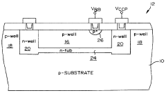
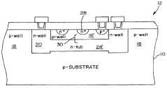
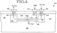
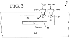
Charge-pumping to increase electron collection efficiency
PatentInactiveUS6111282A
Innovation
- Implementing a charge pumping circuit to increase the bias voltage of n-tubs beyond conventional levels, up to twice the supply voltage, and monitoring the resulting current to dynamically enable or disable charge pumping, ensuring effective electron collection while preventing undesirable leakage.
Electrostatic collecting device, image forming device, and cleaning device
PatentPendingUS20250138468A1
Innovation
- The electrostatic collecting device incorporates a charging unit with an insulating member that rubs against the collecting unit to charge it, and a charge removing unit that contacts the charging unit to remove excess charge, thereby increasing the charge quantity on the collecting unit and enhancing collection performance.
Manufacturing Processes for Optimized Surface Electrodes
The manufacturing of optimized surface electrodes requires precise control over multiple process parameters to achieve high charge collection efficiency. Traditional manufacturing methods often involve photolithography, where a photoresist is applied to a substrate, exposed through a mask, and developed to create electrode patterns. However, recent advancements have introduced more sophisticated techniques that significantly enhance electrode performance.
Physical vapor deposition (PVD) and chemical vapor deposition (CVD) represent cornerstone technologies for electrode fabrication. PVD methods, including sputtering and thermal evaporation, offer excellent control over film thickness and composition. Magnetron sputtering, in particular, has emerged as a preferred technique for creating highly uniform electrode layers with minimal defects, crucial for maximizing charge collection.
Advanced patterning techniques have evolved beyond conventional lithography. Nanoimprint lithography enables the creation of electrodes with feature sizes below 20 nm, significantly increasing the effective surface area for charge collection. Laser direct writing offers maskless patterning capabilities with high precision, allowing for rapid prototyping and customization of electrode geometries to optimize charge collection pathways.
Surface treatment processes play a vital role in electrode optimization. Plasma treatment can modify surface energy and remove contaminants, improving adhesion between electrode materials and substrates. Chemical functionalization introduces specific molecular groups to electrode surfaces, enhancing charge transfer at interfaces. These treatments can reduce recombination losses at electrode boundaries by passivating surface defects.
Quality control measures are essential throughout the manufacturing process. In-line optical inspection systems can detect microscopic defects that might impair electrode performance. Electrical characterization techniques, such as four-point probe measurements and impedance spectroscopy, provide critical feedback on electrode conductivity and interface properties, enabling process optimization.
Recent innovations include roll-to-roll manufacturing for flexible electrodes, allowing continuous production of optimized electrode structures on polymer substrates. This approach significantly reduces production costs while maintaining high performance. Additionally, atomic layer deposition (ALD) has gained prominence for creating ultra-thin, conformal electrode coatings with atomic-level precision, particularly valuable for complex 3D electrode architectures.
The integration of computational modeling with manufacturing processes represents a paradigm shift in electrode optimization. Simulation-guided manufacturing uses predictive models to determine optimal process parameters before physical production begins, reducing iteration cycles and material waste while maximizing charge collection efficiency.
Environmental Impact of Advanced Electrode Materials
The environmental implications of advanced electrode materials used in charge collection optimization represent a critical dimension of sustainable technology development. As surface electrode technologies evolve to improve efficiency, their environmental footprint becomes increasingly significant. Traditional electrode materials often contain rare earth elements, heavy metals, and toxic compounds that pose substantial environmental risks throughout their lifecycle.
Advanced electrode materials designed for enhanced charge collection efficiency frequently incorporate nanomaterials such as carbon nanotubes, graphene, and metal oxide nanoparticles. While these materials offer remarkable performance benefits, their production processes typically demand high energy inputs and generate considerable carbon emissions. For instance, high-purity graphene synthesis can consume up to 100 times more energy than conventional electrode material production, contributing significantly to greenhouse gas emissions.
The extraction of raw materials for next-generation electrodes presents additional environmental challenges. Mining operations for elements like indium, gallium, and rare earth metals cause habitat destruction, soil erosion, and water contamination. Studies indicate that for every ton of rare earth elements extracted, approximately 2,000 tons of toxic waste may be generated, creating long-term environmental liabilities in mining regions.
Water consumption represents another critical environmental concern in electrode manufacturing. Advanced surface electrode fabrication processes, particularly those involving chemical vapor deposition and wet etching techniques, can require between 10-15 liters of ultra-pure water per square centimeter of electrode material. This intensive water usage strains local resources, especially in water-stressed regions where many manufacturing facilities are located.
End-of-life management for advanced electrode materials presents both challenges and opportunities. The complex composition of high-efficiency electrodes often complicates recycling efforts, with recovery rates for critical materials typically below 35%. However, emerging recycling technologies specifically designed for advanced electrode materials show promise, with pilot programs demonstrating recovery rates approaching 70% for certain components.
Encouragingly, some advanced electrode materials offer environmental benefits through extended product lifespans. Optimized surface electrodes can improve device durability by 30-50%, potentially reducing electronic waste generation. Additionally, biomimetic and biodegradable electrode materials represent an emerging frontier, with recent research demonstrating functional electrodes derived from sustainable sources like cellulose and alginate that maintain 80% of conventional performance while dramatically reducing environmental impact.
Unlock deeper insights with Patsnap Eureka Quick Research — get a full tech report to explore trends and direct your research. Try now!
Generate Your Research Report Instantly with AI Agent
Supercharge your innovation with Patsnap Eureka AI Agent Platform!