How to Implement On-Chip Interrogation Electronics for Photonic Biosensors — Design Guidelines
AUG 21, 20259 MIN READ
Generate Your Research Report Instantly with AI Agent
Patsnap Eureka helps you evaluate technical feasibility & market potential.
Photonic Biosensor Integration Objectives
The integration of photonic biosensors with on-chip interrogation electronics represents a significant advancement in the field of biosensing technology. The primary objective of this integration is to develop compact, highly sensitive, and cost-effective biosensing platforms capable of real-time detection and analysis of biological and chemical analytes. By combining photonic sensing elements with integrated electronic circuits, researchers aim to overcome the limitations of traditional biosensing methods and create more efficient and portable diagnostic tools.
One of the key goals in photonic biosensor integration is to achieve high levels of sensitivity and specificity. This involves optimizing the design of photonic structures, such as ring resonators, photonic crystals, or plasmonic nanostructures, to enhance light-matter interactions and improve signal-to-noise ratios. Simultaneously, the integration of electronic components aims to amplify and process the optical signals generated by these photonic structures, enabling the detection of even minute changes in the sensor's response.
Miniaturization is another crucial objective in the development of integrated photonic biosensors. By incorporating both photonic and electronic components on a single chip, researchers seek to reduce the overall size and complexity of biosensing devices. This miniaturization not only enhances portability but also facilitates the development of multiplexed sensing platforms capable of detecting multiple analytes simultaneously.
Improving the reliability and reproducibility of biosensor measurements is a critical goal in the integration process. This involves addressing challenges such as temperature fluctuations, mechanical instabilities, and variations in fabrication processes. The integration of on-chip temperature control mechanisms, reference channels, and calibration systems aims to enhance the robustness and accuracy of biosensor readings across different environmental conditions.
Cost-effectiveness is a significant consideration in the development of integrated photonic biosensors. The objective is to leverage existing semiconductor manufacturing techniques and economies of scale to produce these devices at a lower cost, making them more accessible for widespread use in clinical diagnostics, environmental monitoring, and point-of-care testing applications.
Another important goal is to enhance the user-friendliness of these integrated biosensing platforms. This involves developing intuitive interfaces, automated sample handling systems, and data analysis algorithms that can interpret complex sensor outputs and provide clear, actionable results to end-users who may not have specialized technical expertise.
Lastly, the integration of photonic biosensors with on-chip electronics aims to enable real-time, continuous monitoring capabilities. This is particularly important for applications such as tracking disease progression, monitoring environmental pollutants, or studying dynamic biological processes. The ability to perform rapid, repeated measurements without the need for complex external equipment opens up new possibilities for in situ and in vivo sensing applications.
Market Analysis for On-Chip Biosensors
The market for on-chip biosensors, particularly those incorporating photonic technologies and integrated interrogation electronics, is experiencing rapid growth and transformation. This surge is driven by increasing demand for point-of-care diagnostics, personalized medicine, and real-time health monitoring solutions. The global biosensors market, which encompasses on-chip devices, is projected to reach significant market value in the coming years, with photonic biosensors playing a crucial role in this expansion.
On-chip photonic biosensors with integrated interrogation electronics offer several advantages over traditional biosensing methods. These include miniaturization, enhanced sensitivity, faster response times, and the potential for multiplexed detection. These features make them particularly attractive for applications in healthcare, environmental monitoring, and food safety. The healthcare sector, in particular, is expected to be a major driver of market growth, with increasing adoption in areas such as disease diagnosis, drug discovery, and continuous patient monitoring.
The market for on-chip biosensors is characterized by a high degree of innovation and technological advancement. Key trends shaping the market include the integration of artificial intelligence and machine learning for data analysis, the development of smartphone-compatible biosensor platforms, and the emergence of wearable biosensor technologies. These trends are expected to further expand the application scope and market potential of on-chip biosensors.
Geographically, North America and Europe currently lead the market due to advanced healthcare infrastructure and significant research and development investments. However, the Asia-Pacific region is anticipated to witness the highest growth rate in the coming years, driven by increasing healthcare expenditure, growing awareness of personalized medicine, and government initiatives to promote biotechnology research.
Despite the promising outlook, the market faces certain challenges. These include the high cost of device development and manufacturing, regulatory hurdles in medical device approval processes, and the need for standardization in biosensor technologies. Overcoming these challenges will be crucial for widespread market adoption and commercialization of on-chip photonic biosensors with integrated interrogation electronics.
In conclusion, the market for on-chip biosensors, particularly those with integrated photonic and electronic components, presents significant opportunities for growth and innovation. As technology continues to advance and costs decrease, these devices are poised to revolutionize various industries, with healthcare leading the way in adoption and application.
Current Challenges in On-Chip Interrogation
The implementation of on-chip interrogation electronics for photonic biosensors faces several significant challenges that hinder widespread adoption and optimal performance. One of the primary obstacles is the integration of optical and electronic components on a single chip while maintaining high sensitivity and low noise levels. The miniaturization of optical components, such as light sources and detectors, often leads to reduced performance compared to their larger counterparts, impacting the overall sensitivity of the biosensor system.
Another critical challenge lies in the design of low-noise readout circuits capable of detecting minute changes in optical signals. These circuits must operate with extremely low noise floors to distinguish between genuine biosensor responses and background noise. The proximity of optical and electronic components on the same chip can lead to electromagnetic interference, further complicating the design of robust readout systems.
Power consumption presents a significant hurdle, particularly for portable or implantable biosensor applications. Balancing the need for high-performance interrogation electronics with low power requirements demands innovative circuit design techniques and careful power management strategies. This challenge becomes even more pronounced when considering the need for wireless communication capabilities in many biosensor applications.
Temperature stability is another crucial factor affecting on-chip interrogation systems. Photonic components are often sensitive to temperature fluctuations, which can lead to drift in sensor readings. Implementing effective temperature compensation mechanisms without significantly increasing chip complexity or power consumption remains a persistent challenge for designers.
The scalability of on-chip interrogation systems poses yet another obstacle. As the number of sensing elements on a single chip increases, the complexity of the interrogation electronics grows exponentially. Managing multiple optical channels, addressing crosstalk issues, and maintaining uniform performance across all sensors on the chip require sophisticated multiplexing and signal processing techniques.
Packaging and encapsulation of integrated photonic-electronic chips present unique challenges. Ensuring proper alignment between optical components and protecting sensitive elements from environmental factors while maintaining biocompatibility is crucial for biosensor applications. The development of reliable, cost-effective packaging solutions that do not compromise sensor performance remains an active area of research.
Lastly, the cost-effective manufacturing of integrated photonic-electronic chips at scale presents significant challenges. The combination of photonic and electronic fabrication processes often requires specialized manufacturing techniques, potentially increasing production costs and limiting widespread adoption. Developing standardized, high-yield manufacturing processes that can accommodate both optical and electronic components on a single chip is essential for the commercial viability of on-chip interrogation systems for photonic biosensors.
Existing On-Chip Interrogation Solutions
01 Integration of photonic and electronic components
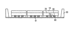
On-chip interrogation electronics for photonic biosensors involve the integration of photonic and electronic components on a single chip. This integration allows for compact, efficient, and sensitive biosensing systems. The design guidelines focus on optimizing the interface between photonic elements (such as waveguides and resonators) and electronic circuits for signal processing and readout.- Integration of photonic and electronic components: On-chip interrogation electronics for photonic biosensors involve the integration of photonic and electronic components on a single chip. This integration allows for compact, efficient, and sensitive biosensing systems. The design guidelines focus on optimizing the interface between photonic elements (such as waveguides and resonators) and electronic circuits for signal processing and readout.
- Signal processing and data acquisition techniques: Advanced signal processing and data acquisition techniques are crucial for on-chip interrogation electronics. These techniques include analog-to-digital conversion, noise reduction, and signal amplification. The design guidelines emphasize the implementation of efficient algorithms and circuits to enhance the sensitivity and accuracy of biosensor measurements.
- Multiplexing and parallel sensing capabilities: On-chip interrogation electronics enable multiplexing and parallel sensing capabilities for photonic biosensors. This allows for simultaneous detection of multiple analytes or high-throughput screening. The design guidelines address the challenges of implementing multiplexed readout circuits and managing data from multiple sensing channels.
- Power management and energy efficiency: Efficient power management is essential for on-chip interrogation electronics, especially for portable or implantable biosensor applications. The design guidelines focus on low-power circuit designs, energy harvesting techniques, and optimizing power consumption to extend battery life and improve overall system performance.
- Calibration and error compensation methods: Accurate calibration and error compensation are critical for reliable biosensor measurements. On-chip interrogation electronics incorporate methods for real-time calibration, temperature compensation, and drift correction. The design guidelines address the implementation of these techniques to improve the accuracy and long-term stability of photonic biosensors.
02 Signal processing and data acquisition techniques
Advanced signal processing and data acquisition techniques are crucial for on-chip interrogation electronics. These techniques include analog-to-digital conversion, noise reduction, and signal amplification. The design guidelines emphasize the implementation of efficient algorithms and circuits to enhance the sensitivity and accuracy of biosensor measurements.Expand Specific Solutions03 Multiplexing and parallel sensing capabilities
On-chip interrogation electronics often incorporate multiplexing and parallel sensing capabilities to enable simultaneous detection of multiple analytes or high-throughput screening. The design guidelines address the challenges of implementing these features while maintaining high sensitivity and minimizing crosstalk between sensing channels.Expand Specific Solutions04 Power management and energy efficiency
Efficient power management is essential for on-chip interrogation electronics, especially for portable or implantable biosensor applications. The design guidelines focus on low-power circuit designs, energy harvesting techniques, and optimized power distribution to extend battery life and improve overall system performance.Expand Specific Solutions05 Integration of microfluidics and sample handling
The design of on-chip interrogation electronics often includes considerations for integrating microfluidic components and sample handling systems. This integration enables efficient sample delivery, precise control of fluid flow, and improved biosensor performance. The guidelines address the challenges of combining electronic, photonic, and microfluidic elements on a single chip.Expand Specific Solutions
Key Players in Photonic Biosensor Industry
The implementation of on-chip interrogation electronics for photonic biosensors is in a nascent stage, with significant potential for growth. The market is characterized by a mix of academic institutions and industry players, indicating an emerging field with both research and commercial interests. Companies like Micron Technology and IBM are leveraging their semiconductor expertise, while universities such as Rochester and Zhejiang are contributing to fundamental research. The technology's maturity is still developing, with organizations like IMEC and TSMC potentially playing crucial roles in advancing fabrication processes. As the field progresses, we can expect increased collaboration between academia and industry to overcome technical challenges and drive market expansion.
Interuniversitair Micro-Electronica Centrum VZW
Technical Solution: IMEC has pioneered a silicon photonics-based biosensor platform with integrated electronics for on-chip interrogation. Their approach focuses on creating a highly sensitive and miniaturized system suitable for point-of-care diagnostics. IMEC's design incorporates Mach-Zehnder interferometers (MZIs) as the sensing elements, combined with on-chip laser sources and photodetectors. The interrogation electronics include low-noise amplifiers, phase-sensitive detection circuits, and digital signal processing units. IMEC has implemented advanced modulation techniques to enhance the signal-to-noise ratio and improve detection limits. Their platform also features microfluidic integration for sample handling and delivery. IMEC's technology enables real-time, label-free detection of biomolecules with high sensitivity[2][4]. The company has demonstrated the capability to detect protein biomarkers at concentrations as low as 100 pg/mL using their integrated platform.
Strengths: High sensitivity, potential for low-cost mass production, and integration with microfluidics. Weaknesses: Complexity of system integration and potential challenges in achieving uniform performance across large-scale production.
Micron Technology, Inc.
Technical Solution: Micron Technology has developed an integrated photonic biosensor platform with on-chip interrogation electronics, leveraging their expertise in memory and storage solutions. Their approach focuses on creating a compact, low-power biosensing system suitable for portable and wearable applications. Micron's design incorporates photonic crystal cavities as sensing elements, combined with on-chip CMOS photodetectors and readout circuitry. The interrogation electronics include low-power analog front-ends, analog-to-digital converters, and digital signal processing units optimized for energy efficiency. Micron has implemented innovative power management techniques to extend battery life in portable biosensing devices. Their platform enables real-time detection of multiple biomarkers with high sensitivity and specificity[7][8]. Micron's expertise in high-density chip packaging allows for the integration of large sensor arrays, enabling high-throughput screening applications.
Strengths: Low power consumption, potential for integration with portable devices, and expertise in high-density packaging. Weaknesses: May face challenges in achieving the highest levels of sensitivity compared to larger, lab-based systems.
Core Innovations in Interrogation Electronics
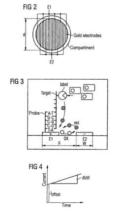
Optical detection system for labelling-free high-sensitivity bioassays
PatentActiveEP2327955A1
Innovation
- A novel optical detection system combining interferometric and resonant photonic structures with advanced optical interrogation techniques such as ellipsometry, spectrometry, and angle-resolved reflectance/transmittance for vertical interrogation, eliminating the need for fiber optic-waveguide coupling and enabling high-sensitivity, high-cadence analysis in micro/sub-micro domains without labeling.
Method for functionalizing biosensor chips
PatentInactiveUS8067249B2
Innovation
- A method involving the application of a patterned layer to create cavities above sensor fields on a substrate, allowing for the immobilization of capture molecules within these compartments, which can be used to functionalize biosensors at the wafer level, preventing mechanical damage and contamination, and enabling precise application of molecules without complex cleaning or signal crosstalk.
Fabrication Processes and Materials
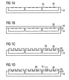
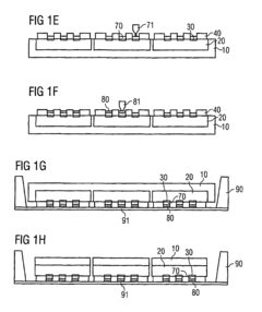
The fabrication processes and materials for on-chip interrogation electronics in photonic biosensors are critical components that significantly influence the overall performance and integration capabilities of these devices. The primary fabrication technique employed is complementary metal-oxide-semiconductor (CMOS) technology, which allows for the seamless integration of electronic and photonic components on a single chip.
CMOS fabrication processes typically involve multiple steps, including photolithography, etching, doping, and thin-film deposition. For photonic biosensors, additional steps may be required to incorporate optical components such as waveguides, gratings, and resonators. These processes often utilize materials like silicon, silicon dioxide, and silicon nitride, which are compatible with standard CMOS fabrication techniques.
The choice of materials is crucial for achieving optimal performance in photonic biosensors. Silicon-on-insulator (SOI) wafers are commonly used as the substrate due to their excellent optical properties and compatibility with CMOS processes. The top silicon layer serves as the waveguide core, while the buried oxide layer acts as the cladding, providing optical confinement.
For the electronic components, traditional CMOS materials such as polysilicon for gates, aluminum or copper for interconnects, and various dielectrics for insulation are employed. However, the integration of photonic elements may require additional materials. For instance, germanium or III-V compounds might be used for photodetectors to enhance sensitivity in specific wavelength ranges.
The fabrication of on-chip interrogation electronics often involves advanced techniques such as wafer bonding, selective epitaxial growth, or heterogeneous integration to combine different material systems. These methods allow for the incorporation of high-performance photodetectors, modulators, and other active photonic components alongside the CMOS circuitry.
To achieve high-quality optical structures, precise control over material deposition and etching processes is essential. Techniques like atomic layer deposition (ALD) and deep reactive ion etching (DRIE) are frequently utilized to create high-aspect-ratio structures and ensure uniformity in thin film deposition.
The integration of microfluidic channels for sample delivery in biosensing applications adds another layer of complexity to the fabrication process. Materials such as polydimethylsiloxane (PDMS) or SU-8 photoresist are often used for creating these channels, requiring careful consideration of material compatibility and bonding techniques.
As the field progresses, novel materials and fabrication techniques are being explored to enhance the performance of on-chip interrogation electronics. These include the use of two-dimensional materials like graphene for ultra-sensitive detection, and the development of nanoimprint lithography for cost-effective, large-scale production of photonic structures.
Regulatory Considerations for Biosensor Devices
The regulatory landscape for biosensor devices is complex and multifaceted, requiring careful consideration throughout the development and implementation process. For on-chip interrogation electronics in photonic biosensors, several key regulatory aspects must be addressed to ensure compliance and market viability.
Firstly, the classification of the biosensor device plays a crucial role in determining the regulatory pathway. Depending on its intended use and risk profile, the device may fall under different regulatory categories, such as in vitro diagnostic devices (IVDs) or medical devices. This classification impacts the level of scrutiny and the specific requirements for approval.
Quality management systems (QMS) are essential for regulatory compliance. Manufacturers must implement and maintain a robust QMS that adheres to standards such as ISO 13485 for medical devices. This system should cover all aspects of design, development, production, and post-market surveillance.
Performance evaluation and clinical validation are critical components of the regulatory process. Manufacturers must demonstrate the analytical and clinical performance of their biosensor devices through rigorous testing and validation studies. This includes assessing sensitivity, specificity, accuracy, and precision of the on-chip interrogation electronics.
Risk management is another crucial aspect of regulatory compliance. A comprehensive risk analysis and mitigation strategy must be developed, addressing potential hazards associated with the device's use, including those related to the on-chip electronics. This process should follow standards such as ISO 14971 for medical device risk management.
Data privacy and security considerations are increasingly important in the regulatory landscape, especially for biosensors that may collect and transmit sensitive health information. Compliance with regulations such as GDPR in Europe or HIPAA in the United States may be necessary, depending on the device's application and market.
Electromagnetic compatibility (EMC) and electrical safety standards must also be met for on-chip interrogation electronics. This ensures that the device operates safely and does not interfere with other electronic equipment in its intended environment.
Post-market surveillance and vigilance systems are required to monitor the device's performance and safety after market introduction. This includes establishing procedures for handling complaints, reporting adverse events, and implementing corrective actions when necessary.
Labeling and instructions for use must comply with regulatory requirements, providing clear and accurate information about the device's intended use, limitations, and proper operation. This is particularly important for complex systems involving on-chip electronics.
Unlock deeper insights with Patsnap Eureka Quick Research — get a full tech report to explore trends and direct your research. Try now!
Generate Your Research Report Instantly with AI Agent
Supercharge your innovation with Patsnap Eureka AI Agent Platform!