How to Integrate Photonic Crystal Sensors into Point-of-Care Devices — Packaging & Readout
AUG 21, 20259 MIN READ
Generate Your Research Report Instantly with AI Agent
Patsnap Eureka helps you evaluate technical feasibility & market potential.
Photonic Crystal Sensors in POC: Background and Objectives
Photonic crystal sensors have emerged as a promising technology for point-of-care (POC) devices, offering high sensitivity, label-free detection, and real-time monitoring capabilities. These sensors leverage the unique optical properties of photonic crystals, which are periodic nanostructures that can manipulate light at the nanoscale. The integration of photonic crystal sensors into POC devices represents a significant advancement in portable diagnostic tools, potentially revolutionizing healthcare delivery in resource-limited settings.
The development of photonic crystal sensors for POC applications has been driven by the increasing demand for rapid, accurate, and cost-effective diagnostic tools. Traditional laboratory-based tests often require sophisticated equipment, trained personnel, and lengthy processing times, which are not suitable for on-site or immediate diagnostics. POC devices aim to address these limitations by providing quick results at the patient's location, enabling timely decision-making and improved patient outcomes.
The evolution of photonic crystal sensor technology can be traced back to the late 1980s when the concept of photonic bandgap materials was first introduced. Since then, significant progress has been made in fabrication techniques, materials science, and optical detection methods, leading to the current state of photonic crystal sensors suitable for POC integration.
The primary objective of integrating photonic crystal sensors into POC devices is to create compact, user-friendly, and highly sensitive diagnostic tools that can detect a wide range of biomarkers, pathogens, or environmental contaminants. This integration faces several challenges, particularly in the areas of packaging and readout systems. Packaging must ensure the sensor's stability, protection from environmental factors, and compatibility with biological samples, while maintaining optical access to the sensing surface.
Readout systems for photonic crystal sensors in POC devices need to be miniaturized, robust, and capable of translating optical signals into meaningful diagnostic information. This often involves the development of specialized optoelectronic components and data processing algorithms tailored for portable applications.
The successful integration of photonic crystal sensors into POC devices has the potential to address critical healthcare needs in various settings, from remote rural areas to urban emergency departments. By providing rapid and accurate diagnostics, these devices could enable early disease detection, monitoring of treatment efficacy, and timely intervention in public health crises.
As research in this field progresses, the focus is on overcoming technical hurdles related to sensor fabrication, integration, and readout optimization. The ultimate goal is to develop reliable, cost-effective POC devices that can perform complex diagnostic tests with accuracy comparable to laboratory-based methods, while offering the advantages of portability and ease of use.
Market Analysis for POC Photonic Crystal Devices
The market for point-of-care (POC) photonic crystal devices is experiencing significant growth, driven by the increasing demand for rapid, accurate, and cost-effective diagnostic solutions. This emerging technology combines the sensitivity of photonic crystals with the convenience of POC testing, offering potential advantages in various healthcare settings.
The global POC diagnostics market, which encompasses photonic crystal devices, is projected to reach substantial value in the coming years. This growth is fueled by factors such as the rising prevalence of infectious diseases, the need for quick and reliable diagnostic tools, and the shift towards personalized medicine. Photonic crystal-based POC devices are poised to capture a growing share of this market due to their unique capabilities.
One of the key drivers for POC photonic crystal devices is their potential to provide highly sensitive and specific results in a compact, portable format. This aligns well with the increasing trend towards decentralized healthcare and the need for rapid diagnostics in resource-limited settings. The technology's ability to detect biomarkers at low concentrations makes it particularly attractive for early disease detection and monitoring.
The healthcare sector represents the primary market for POC photonic crystal devices, with applications spanning infectious disease diagnostics, cancer screening, and monitoring of chronic conditions. Within this sector, hospitals, clinics, and physician offices are expected to be major adopters of the technology. Additionally, there is growing interest from the pharmaceutical industry for drug development and personalized medicine applications.
Geographically, North America and Europe are currently the leading markets for POC photonic crystal devices, owing to their advanced healthcare infrastructure and higher adoption rates of new technologies. However, emerging economies in Asia-Pacific and Latin America present significant growth opportunities due to their large populations and increasing healthcare expenditure.
Despite the promising outlook, the market for POC photonic crystal devices faces several challenges. These include the need for standardization, regulatory hurdles, and competition from established diagnostic technologies. Overcoming these barriers will be crucial for widespread adoption and market penetration.
In terms of market dynamics, both large medical device companies and innovative startups are actively developing POC photonic crystal technologies. This competitive landscape is likely to drive further innovation and potentially lead to strategic partnerships or acquisitions as the market matures.
Current Challenges in Photonic Crystal Sensor Integration
The integration of photonic crystal sensors into point-of-care devices faces several significant challenges, primarily in the areas of packaging and readout. One of the main obstacles is miniaturization while maintaining sensor performance. Photonic crystal sensors often require precise optical alignment and stable environmental conditions, which can be difficult to achieve in compact, portable devices. The packaging must protect the sensitive photonic crystal structure from external factors such as temperature fluctuations, mechanical stress, and chemical contamination, all of which can affect sensor accuracy and reliability.
Another critical challenge is the development of efficient and cost-effective readout systems. Traditional spectroscopic equipment used for photonic crystal sensor analysis is often bulky and expensive, making it unsuitable for point-of-care applications. Integrating compact light sources, detectors, and signal processing components without compromising sensitivity and specificity is a complex task. Additionally, the readout system must be capable of real-time data acquisition and analysis to provide rapid results in clinical settings.
The interface between the photonic crystal sensor and the sample delivery system presents further complications. Ensuring consistent and controlled sample introduction while preventing contamination or degradation of the sensor surface is crucial. This becomes particularly challenging when dealing with complex biological samples such as blood or saliva, which may require additional preprocessing steps.
Power management is another significant hurdle in integrating photonic crystal sensors into portable devices. The optical components and signal processing units often have high power requirements, which can limit the device's operational time and portability. Developing energy-efficient alternatives or innovative power solutions is essential for creating truly mobile point-of-care devices.
Standardization and calibration of integrated photonic crystal sensors pose additional challenges. Ensuring consistent performance across different devices and maintaining accuracy over time requires robust calibration protocols and quality control measures. This is particularly important in clinical settings where reliable and reproducible results are critical for patient care.
Lastly, the manufacturing process for integrating photonic crystal sensors into point-of-care devices must be scalable and cost-effective. Current fabrication methods for photonic crystals often involve complex and expensive techniques, which can be a barrier to widespread adoption. Developing simplified manufacturing processes that maintain sensor quality while reducing production costs is crucial for the commercial viability of these integrated devices.
Existing Packaging Solutions for Photonic Crystal Sensors
01 Optical readout systems for photonic crystal sensors
Various optical readout systems are designed for photonic crystal sensors. These systems may include spectrometers, photodetectors, and imaging devices to capture and analyze the optical response of the photonic crystal. Advanced readout techniques can improve sensitivity and accuracy in detecting changes in the photonic crystal structure due to external stimuli.- Optical readout systems for photonic crystal sensors: Various optical readout systems are designed for photonic crystal sensors, including spectroscopic and imaging-based approaches. These systems often incorporate light sources, detectors, and optical components to measure changes in the photonic crystal's optical properties in response to environmental stimuli.
- Integration of photonic crystal sensors with optical fibers: Photonic crystal sensors can be integrated with optical fibers for remote sensing applications. This approach allows for compact packaging and efficient light coupling between the sensor and the readout system, enabling distributed sensing in various environments.
- Packaging techniques for photonic crystal sensors: Various packaging techniques are employed to protect photonic crystal sensors from environmental factors while maintaining their sensitivity. These may include encapsulation methods, protective coatings, and integration with microfluidic systems for sample handling and delivery.
- Miniaturization and integration of photonic crystal sensor systems: Efforts are made to miniaturize and integrate photonic crystal sensor systems for portable and on-chip applications. This involves the development of compact light sources, detectors, and signal processing components, as well as the integration of multiple sensors on a single chip.
- Signal processing and data analysis for photonic crystal sensors: Advanced signal processing and data analysis techniques are developed to enhance the performance of photonic crystal sensors. These methods may include noise reduction algorithms, pattern recognition, and machine learning approaches to improve sensor sensitivity, selectivity, and reliability.
02 Packaging techniques for photonic crystal sensors
Packaging methods for photonic crystal sensors focus on protecting the sensitive structures while allowing interaction with the target analytes. Techniques may include encapsulation in transparent materials, integration with microfluidic channels, or incorporation into fiber optic systems. Proper packaging is crucial for maintaining sensor performance and durability in various applications.Expand Specific Solutions03 Integration of photonic crystal sensors with electronic components
Photonic crystal sensors are often integrated with electronic components for signal processing and data transmission. This integration may involve coupling the optical output to photodetectors, incorporating analog-to-digital converters, and implementing signal amplification circuits. The combination of photonic and electronic elements enables compact and efficient sensing systems.Expand Specific Solutions04 Fabrication methods for photonic crystal sensor arrays
Advanced fabrication techniques are employed to create arrays of photonic crystal sensors. These methods may include lithography, etching, and deposition processes to produce multiple sensing elements on a single substrate. Array configurations allow for multiplexed sensing and improved spatial resolution in various applications.Expand Specific Solutions05 Signal processing and data analysis for photonic crystal sensors
Sophisticated signal processing and data analysis techniques are developed to interpret the output from photonic crystal sensors. These may include algorithms for spectral analysis, pattern recognition, and noise reduction. Advanced data processing methods enhance the sensitivity, selectivity, and reliability of photonic crystal sensor systems in complex environments.Expand Specific Solutions
Key Players in Photonic Crystal POC Industry
The integration of photonic crystal sensors into point-of-care devices is an emerging field at the intersection of photonics and healthcare. This technology is in its early development stage, with significant potential for growth in the coming years. The market size is expected to expand rapidly as the demand for portable, rapid, and sensitive diagnostic tools increases. Companies like X-Body, Abbott Point of Care, and SRU Biosystems are at the forefront of this technology, focusing on developing innovative packaging and readout solutions. The technical maturity varies, with some aspects well-established and others still requiring substantial research. Collaborations between academic institutions like the University of Illinois and industry players are driving advancements in sensor integration and miniaturization, crucial for successful point-of-care applications.
Abbott Point of Care, Inc.
Technical Solution: Abbott Point of Care has developed an integrated photonic crystal biosensor platform for point-of-care diagnostics. Their approach utilizes a label-free, high-sensitivity photonic crystal surface that can be functionalized for specific biomarker detection. The readout system employs a compact, low-cost optical setup with a CMOS image sensor for signal detection. Abbott's packaging solution integrates the photonic crystal sensor with microfluidics for sample handling and a miniaturized readout system, all contained within a portable device suitable for point-of-care use[1][3]. The system achieves rapid results, typically within 5-15 minutes, with high sensitivity comparable to laboratory-based methods[2].
Strengths: High sensitivity, rapid results, and integration of sample handling. Weaknesses: May require specialized manufacturing processes for the photonic crystal sensors, potentially increasing production costs.
SRU Biosystems, Inc.
Technical Solution: SRU Biosystems has pioneered the development of BIND (Biomolecular Interaction Detection) technology, which incorporates photonic crystal sensors into microplate-based assays for point-of-care applications. Their approach uses a proprietary nanostructured surface that functions as a photonic crystal, providing label-free, real-time detection of biomolecular interactions. The readout system employs a spectrometer to measure the shift in reflected wavelength caused by binding events on the sensor surface. SRU's packaging solution integrates the photonic crystal sensors into standard microplate formats, allowing for easy adoption in existing laboratory workflows and point-of-care settings[4]. The system can detect binding events with high sensitivity, down to picogram/mm² levels, and provides kinetic information about molecular interactions[5].
Strengths: High sensitivity, compatibility with existing lab equipment, and ability to provide kinetic data. Weaknesses: May require more complex readout instrumentation compared to simpler colorimetric tests.
Innovative Readout Mechanisms for Photonic Crystals
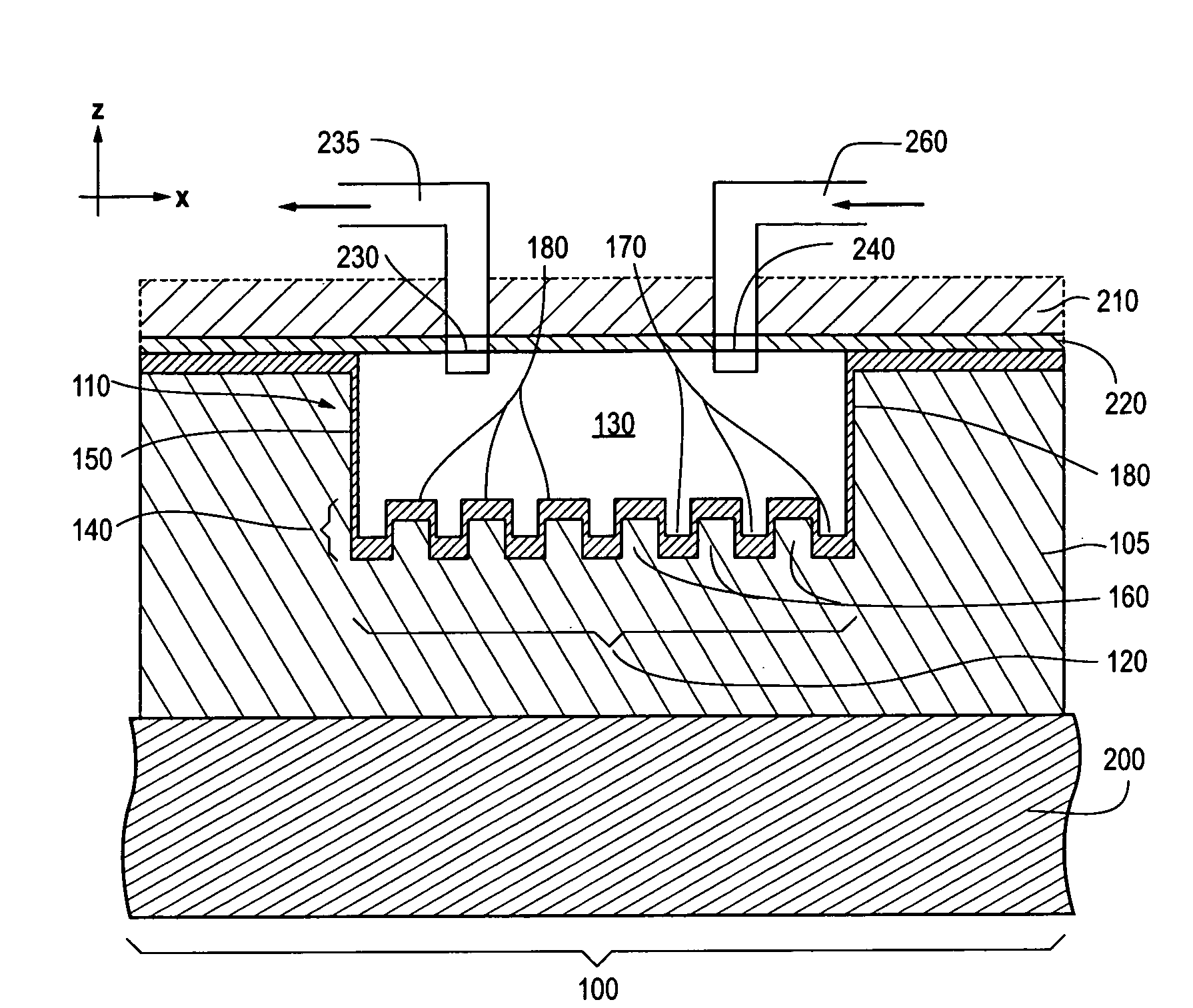
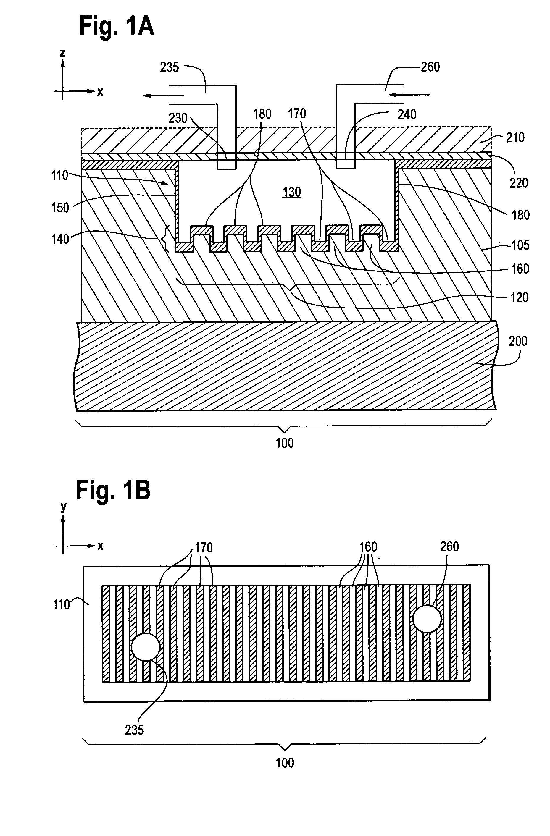
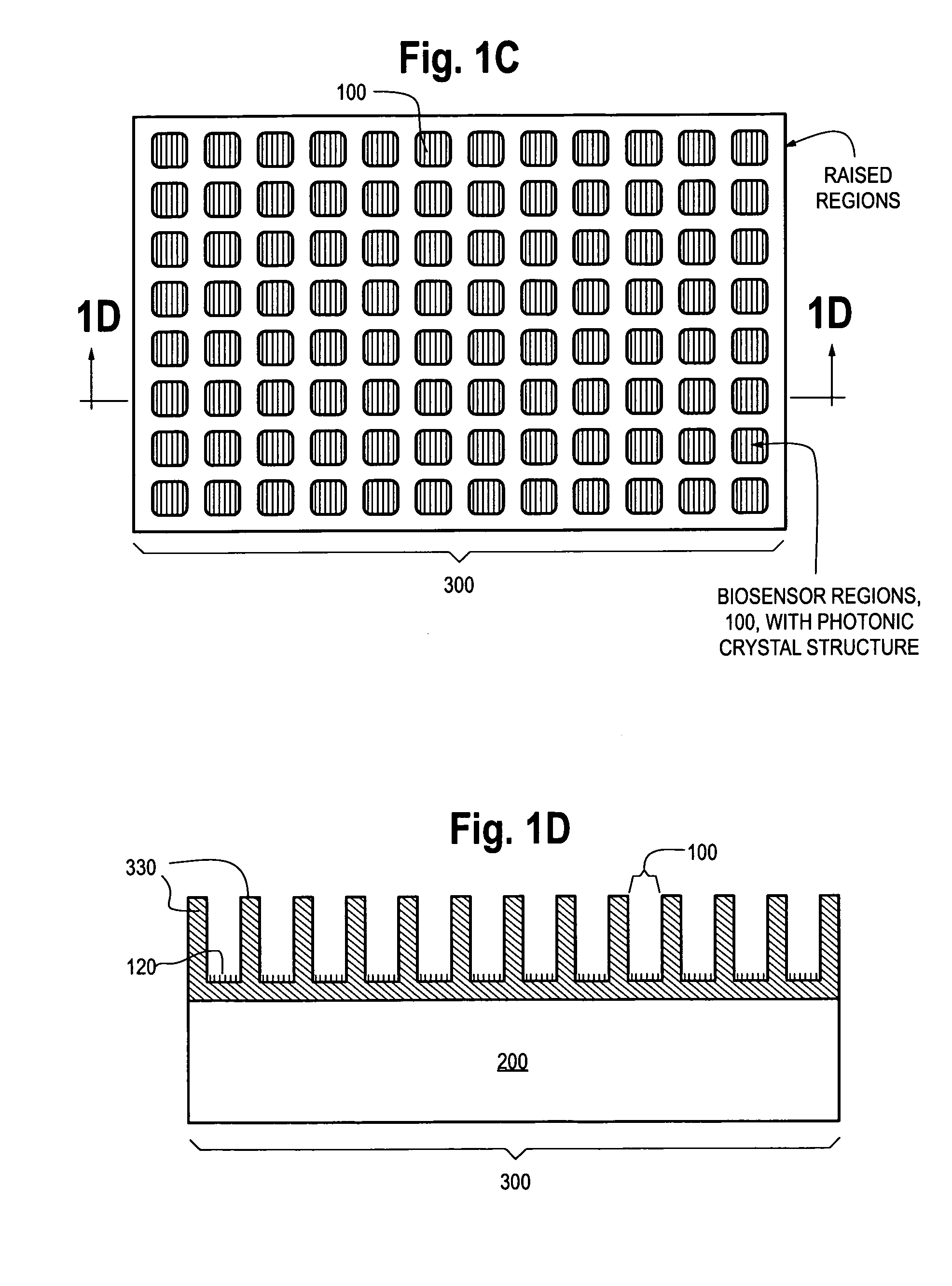
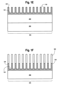
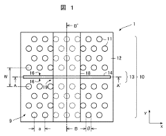
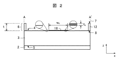
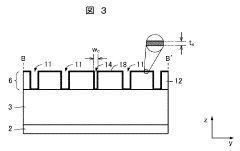
Photonic crystal sensors with integrated fluid containment structure, sample handling devices incorporating same, and uses thereof for biomolecular interaction analysis
PatentActiveUS20090079976A1
Innovation
- The integration of photonic crystal sensors with fluid containment structures in a monolithic structure, where the photonic crystal surface grating is part of the internal surface of the fluid containment structure, allowing for simultaneous fabrication and alignment, reducing the risk of damage and interference, and enabling cost-effective, high-throughput manufacturing using techniques like replica molding and imprint lithography.
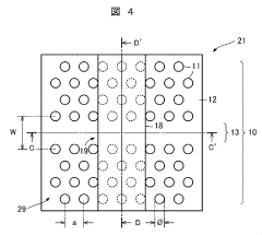
Photonic crystal-based sensor
PatentActiveJP2023042512A
Innovation
- A photonic crystal-based sensor with a waveguide and strip cavities formed by inkjet printing using femtoliter droplets, allowing for high-resolution deposition of probe molecules without the need for precise alignment, and incorporating slots or thicker biocompatible layers to enhance sensitivity and multiplexing.
Miniaturization Strategies for POC Photonic Devices
Miniaturization strategies for point-of-care (POC) photonic devices are crucial for integrating photonic crystal sensors into compact, portable diagnostic tools. These strategies focus on reducing the overall size and complexity of the sensing system while maintaining or enhancing its performance.
One key approach involves the development of integrated optoelectronic components. By combining light sources, detectors, and signal processing elements on a single chip, researchers can significantly reduce the footprint of photonic devices. This integration often leverages complementary metal-oxide-semiconductor (CMOS) technology, enabling the fabrication of compact, low-cost sensors suitable for POC applications.
Another important strategy is the optimization of photonic crystal structures for miniaturization. This includes the design of high-quality factor resonators with smaller dimensions, which can enhance sensitivity while reducing the overall device size. Advanced fabrication techniques, such as nanoimprint lithography and electron-beam lithography, play a crucial role in creating these intricate nanostructures with high precision.
Microfluidic integration is also essential for miniaturizing POC photonic devices. By incorporating microfluidic channels directly into the photonic crystal sensor platform, researchers can achieve efficient sample handling and reduce the required sample volume. This integration not only contributes to device miniaturization but also improves the overall sensitivity and speed of analysis.
The development of compact readout systems is another critical aspect of miniaturization. This involves the design of low-power, high-sensitivity photodetectors and the implementation of efficient signal processing algorithms. Advanced packaging techniques, such as 3D integration and system-in-package approaches, further contribute to reducing the overall size of the readout electronics.
Lastly, the use of flexible and stretchable materials in photonic crystal sensor fabrication opens up new possibilities for miniaturization. These materials allow for the creation of conformal sensors that can adapt to various surfaces and form factors, making them ideal for wearable POC devices and other space-constrained applications.
Regulatory Considerations for Photonic Crystal POC Devices
The integration of photonic crystal sensors into point-of-care (POC) devices presents unique regulatory challenges that must be carefully addressed to ensure compliance and market approval. Regulatory bodies such as the FDA in the United States and the EMA in Europe have established stringent guidelines for medical devices, particularly those intended for diagnostic use at the point of care.
One of the primary regulatory considerations for photonic crystal POC devices is their classification. Depending on the intended use and risk level, these devices may fall under Class II or Class III medical devices, requiring different levels of regulatory scrutiny. Manufacturers must conduct a thorough risk assessment to determine the appropriate classification and regulatory pathway.
Safety and efficacy are paramount concerns for regulatory bodies. Developers of photonic crystal POC devices must provide comprehensive data demonstrating the device's safety profile, including potential risks associated with the use of photonic crystals and any packaging materials. Efficacy studies should demonstrate the device's accuracy, precision, and clinical utility in real-world settings.
Quality control and manufacturing processes are also subject to regulatory oversight. Manufacturers must implement and maintain robust quality management systems that comply with ISO 13485 standards for medical devices. This includes establishing procedures for design control, risk management, and post-market surveillance.
Data privacy and security are increasingly important regulatory considerations, especially for POC devices that may collect and transmit patient data. Developers must ensure compliance with regulations such as HIPAA in the United States and GDPR in Europe, implementing appropriate safeguards to protect sensitive health information.
Usability and human factors engineering play a crucial role in regulatory approval. Manufacturers must demonstrate that their photonic crystal POC devices can be safely and effectively used by the intended operators, which may include healthcare professionals or patients themselves. This requires comprehensive usability testing and validation studies.
Environmental impact and sustainability are emerging regulatory concerns. Developers should consider the environmental footprint of their devices, including the use of recyclable materials and energy-efficient components, to align with evolving regulatory expectations and sustainability goals.
Lastly, regulatory requirements for photonic crystal POC devices may vary across different regions and countries. Manufacturers aiming for global market access must navigate these diverse regulatory landscapes, potentially requiring multiple submissions and approvals to ensure compliance in each target market.
Unlock deeper insights with Patsnap Eureka Quick Research — get a full tech report to explore trends and direct your research. Try now!
Generate Your Research Report Instantly with AI Agent
Supercharge your innovation with Patsnap Eureka AI Agent Platform!