Low-Cost Replication Methods for Photonic Nanostructures: Nanoimprint and Molding
AUG 21, 20259 MIN READ
Generate Your Research Report Instantly with AI Agent
Patsnap Eureka helps you evaluate technical feasibility & market potential.
Photonic Nanostructure Replication Background
Photonic nanostructures have emerged as a pivotal technology in the field of optics and photonics, offering unprecedented control over light-matter interactions at the nanoscale. These structures, typically featuring intricate patterns with dimensions smaller than the wavelength of light, have found applications in diverse areas such as solar cells, light-emitting diodes, sensors, and optical communication devices.
The replication of photonic nanostructures has been a subject of intense research and development over the past few decades. Initially, the fabrication of these structures relied heavily on expensive and time-consuming techniques such as electron-beam lithography and focused ion beam milling. While these methods offered high precision and resolution, they were not suitable for large-scale production or cost-effective manufacturing.
As the demand for photonic nanostructures grew, researchers and engineers began exploring alternative fabrication methods that could combine high fidelity with scalability and cost-effectiveness. This pursuit led to the development of various replication techniques, with nanoimprint lithography and molding emerging as particularly promising approaches.
Nanoimprint lithography, first introduced in the mid-1990s, involves the mechanical deformation of a polymer resist using a patterned mold. This technique quickly gained attention due to its ability to replicate features with dimensions as small as a few nanometers over large areas. The process typically involves pressing a hard mold into a soft polymer layer, followed by curing and mold removal.
Molding techniques, on the other hand, encompass a broader range of methods including soft lithography, replica molding, and template-assisted self-assembly. These approaches often utilize elastomeric materials like polydimethylsiloxane (PDMS) to create flexible molds that can replicate nanostructures with high fidelity. Molding techniques have proven particularly versatile, allowing for the replication of complex 3D nanostructures that are challenging to produce using traditional lithographic methods.
The development of these low-cost replication methods has been driven by the need to bridge the gap between laboratory-scale fabrication and industrial-scale production of photonic nanostructures. By enabling the rapid and cost-effective replication of nanopatterns, these techniques have opened up new possibilities for the widespread integration of photonic nanostructures into commercial devices and applications.
Market Analysis for Low-Cost Nanofabrication
The market for low-cost nanofabrication techniques, particularly focusing on photonic nanostructures, has been experiencing significant growth in recent years. This surge is driven by the increasing demand for cost-effective manufacturing processes in various industries, including electronics, photonics, and biomedical applications. The global market for nanoimprint lithography, a key technology in this field, was valued at $52 million in 2020 and is projected to reach $120 million by 2026, growing at a CAGR of 15.2% during the forecast period.
The adoption of low-cost replication methods for photonic nanostructures, such as nanoimprint and molding, is gaining traction due to their ability to produce high-resolution patterns at a fraction of the cost of traditional lithography techniques. These methods offer significant advantages in terms of throughput, scalability, and material versatility, making them attractive for both research and industrial applications.
One of the primary drivers for market growth is the expanding application of photonic nanostructures in areas such as optical sensors, displays, and solar cells. The global photonics market, which heavily relies on nanostructured components, is expected to reach $837 billion by 2025, with a CAGR of 7.5%. This growth directly impacts the demand for low-cost nanofabrication techniques.
The semiconductor industry, a major consumer of nanofabrication technologies, is also contributing to market expansion. As the industry continues to push for smaller and more efficient devices, the need for cost-effective nanoscale patterning solutions becomes increasingly critical. The global semiconductor market is projected to reach $726 billion by 2027, creating substantial opportunities for low-cost nanofabrication methods.
Emerging applications in fields such as metamaterials, plasmonics, and quantum technologies are opening new avenues for market growth. These cutting-edge areas require precise control over nanostructures, which can be achieved through advanced replication techniques. The metamaterials market alone is expected to grow at a CAGR of 63.1% from 2020 to 2025, highlighting the potential for low-cost nanofabrication methods in emerging technologies.
Geographically, Asia-Pacific is expected to dominate the market for low-cost nanofabrication, driven by the strong presence of semiconductor and electronics manufacturing industries in countries like China, South Korea, and Taiwan. North America and Europe are also significant markets, with a focus on research and development in advanced materials and photonics applications.
Current Challenges in Nanostructure Replication
Despite significant advancements in nanofabrication techniques, the replication of photonic nanostructures still faces several challenges that hinder widespread adoption and commercialization. One of the primary obstacles is achieving high-fidelity replication across large areas while maintaining cost-effectiveness. Current methods often struggle to balance precision and scalability, particularly when dealing with complex three-dimensional nanostructures.
Material limitations pose another significant challenge. The selection of appropriate materials for both the master mold and the replicated structure is crucial. These materials must possess specific optical, mechanical, and chemical properties to ensure accurate replication and desired functionality of the final photonic devices. Finding materials that meet all these requirements while remaining compatible with low-cost manufacturing processes is an ongoing challenge.
Durability and wear of master molds present a persistent issue, especially in high-volume production scenarios. The repeated use of molds can lead to degradation of nanostructures, affecting the quality and consistency of replicated patterns. This necessitates frequent mold replacement, which increases production costs and reduces overall efficiency.
Alignment and registration accuracy remain critical challenges, particularly for multi-layer or multi-step replication processes. Achieving precise alignment between different layers or patterns is essential for many photonic applications but becomes increasingly difficult as feature sizes decrease and pattern complexity increases.
The removal of residual layers and the complete filling of high-aspect-ratio nanostructures continue to be problematic. Incomplete pattern transfer or the presence of residual materials can significantly impact the optical performance of the replicated structures. Developing techniques to ensure complete pattern transfer without damaging delicate nanostructures is an area of ongoing research.
Environmental factors, such as temperature fluctuations and humidity, can affect the replication process and the stability of replicated structures. Controlling these variables in a manufacturing environment to ensure consistent, high-quality replication remains challenging, especially for large-scale production.
Lastly, the integration of replicated nanostructures into functional devices presents its own set of challenges. This includes issues related to interfacing with other components, maintaining structural integrity during subsequent processing steps, and ensuring long-term stability under various operating conditions.
Addressing these challenges requires interdisciplinary approaches, combining advances in materials science, process engineering, and nanofabrication techniques. Overcoming these hurdles is crucial for realizing the full potential of low-cost replication methods for photonic nanostructures and enabling their widespread application in various fields.
Existing Low-Cost Replication Methods
01 Cost-effective fabrication methods
Various techniques have been developed to reduce the cost of producing photonic nanostructures. These include using self-assembly processes, nanoimprint lithography, and template-assisted methods. These approaches aim to simplify the manufacturing process and reduce the need for expensive equipment, thereby lowering overall production costs.- Cost-effective fabrication methods: Various cost-effective fabrication methods have been developed for producing photonic nanostructures. These include techniques such as nanoimprint lithography, self-assembly processes, and template-assisted methods. These approaches aim to reduce production costs while maintaining the desired optical properties of the nanostructures.
- Materials selection for cost optimization: The choice of materials plays a crucial role in determining the cost of photonic nanostructures. Researchers are exploring the use of low-cost materials, such as polymers and certain semiconductors, to replace expensive traditional materials without compromising performance. This approach can significantly reduce overall production costs.
- Scalable production techniques: Developing scalable production techniques is essential for reducing the cost of photonic nanostructures. Methods such as roll-to-roll processing, large-area patterning, and continuous flow production are being investigated to increase manufacturing efficiency and lower costs for mass production.
- Integration with existing manufacturing processes: Integrating the production of photonic nanostructures with existing semiconductor manufacturing processes can help reduce overall costs. This approach leverages established infrastructure and expertise, minimizing the need for new, specialized equipment and facilities.
- Design optimization for cost reduction: Optimizing the design of photonic nanostructures can lead to cost savings. This includes simplifying structures, reducing the number of layers or components, and designing for easier manufacturing. Advanced simulation and modeling techniques are used to achieve optimal performance with cost-effective designs.
02 Materials selection for cost reduction
Choosing appropriate materials can significantly impact the cost of photonic nanostructures. Researchers are exploring the use of low-cost, abundant materials such as silicon, polymers, and certain metal oxides. These materials can offer similar optical properties to more expensive alternatives while reducing overall production expenses.Expand Specific Solutions03 Scale-up and mass production techniques
Developing methods for large-scale production of photonic nanostructures is crucial for reducing costs. Techniques such as roll-to-roll processing, continuous flow reactors, and automated assembly lines are being explored to increase production volume while maintaining quality and reducing per-unit costs.Expand Specific Solutions04 Integration with existing manufacturing processes
Integrating the production of photonic nanostructures into existing semiconductor or optoelectronic manufacturing processes can help reduce overall costs. This approach leverages existing infrastructure and expertise, minimizing the need for separate, specialized production facilities.Expand Specific Solutions05 Design optimization for cost-efficiency
Optimizing the design of photonic nanostructures can lead to cost savings. This includes developing structures that require fewer processing steps, use less material, or have relaxed tolerance requirements. Computational modeling and machine learning techniques are being employed to identify cost-effective designs that maintain desired optical properties.Expand Specific Solutions
Key Players in Nanofabrication Industry
The field of low-cost replication methods for photonic nanostructures is in a growth phase, with increasing market potential as nanoimprint and molding technologies mature. The global market for these technologies is expanding, driven by applications in electronics, optics, and biomedical sectors. Key players like FUJIFILM Corp., Samsung Electronics, and United Microelectronics Corp. are investing in research and development to improve process efficiency and scalability. Academic institutions such as the University of Massachusetts and Nanjing University are contributing to technological advancements. While the technology is progressing, challenges in large-scale manufacturing and material limitations persist, indicating room for further innovation and market development.
FUJIFILM Corp.
Technical Solution: FUJIFILM has developed a proprietary nanoimprint lithography (NIL) technology called "Simultaneous Thermal and UV Imprint" (STUI). This innovative approach combines thermal and UV curing processes to achieve high-fidelity pattern transfer of photonic nanostructures[1]. The STUI method utilizes a transparent mold and UV-curable resins, allowing for rapid curing and improved throughput compared to traditional thermal NIL[2]. FUJIFILM's technology enables the replication of complex 3D nanostructures with feature sizes down to 10 nm, making it suitable for various photonic applications such as optical waveguides, gratings, and metasurfaces[3]. The company has also developed specialized UV-curable resins optimized for optical properties and durability in photonic devices.
Strengths: Rapid curing process, high-resolution patterning, and compatibility with various substrate materials. Weaknesses: Potential limitations in mold durability and challenges in scaling up for high-volume production.
Agency for Science, Technology & Research
Technical Solution: The Agency for Science, Technology & Research (A*STAR) in Singapore has developed innovative approaches for low-cost replication of photonic nanostructures. Their research focuses on combining nanoimprint lithography (NIL) with novel materials and processes to enhance the efficiency and scalability of nanostructure replication[1]. A*STAR has pioneered the use of hybrid organic-inorganic materials for NIL, which offer improved mechanical and optical properties compared to traditional polymer resists[2]. The agency has also developed a roll-to-roll NIL process for continuous fabrication of large-area photonic nanostructures on flexible substrates, enabling high-throughput production of optical films and devices[3]. Additionally, A*STAR researchers have explored the use of self-assembled block copolymers as templates for nanoimprinting, allowing for the creation of complex 3D photonic nanostructures with sub-10 nm features[4].
Strengths: Innovative material development, scalable roll-to-roll processes, and integration of self-assembly techniques. Weaknesses: Potential challenges in commercialization and technology transfer to industry partners.
Core Innovations in Nanoimprint and Molding
Optical discs as low-cost, quasi-random nanoimprinting templates for photon management
PatentActiveUS10134989B2
Innovation
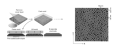
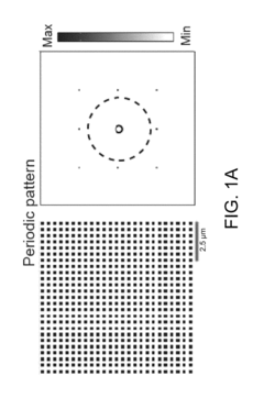
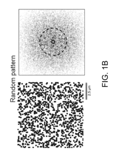
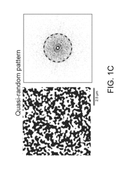
- The use of stamps derived from pre-written optical media discs, such as Blu-ray discs, to imprint quasi-random patterns onto photonic devices, offering a cost-effective and scalable alternative by leveraging the existing mass-produced optical media discs with pre-defined quasi-random nanostructures.
Substrate preparation method, nanoimprint lithography method and mold replication method
PatentInactiveJPWO2010090088A1
Innovation
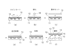
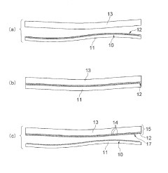
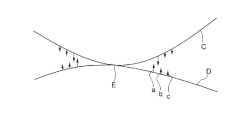
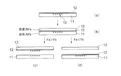
- A method involving the formation of a hardened transfer material layer on a mold, which is then adhered to a substrate without intermediaries, allowing for uniform transfer of the mold structure across the substrate's surface, regardless of its flatness, through physical interaction and self-adsorption.
Environmental Impact of Nanofabrication Processes
The environmental impact of nanofabrication processes, particularly in the context of low-cost replication methods for photonic nanostructures, is a critical consideration in the development and implementation of these technologies. Nanoimprint lithography and molding techniques, while offering cost-effective solutions for mass production, also present unique environmental challenges that must be addressed.
One of the primary environmental concerns associated with these processes is the use of potentially hazardous chemicals and materials. Many nanoimprint resists and mold release agents contain volatile organic compounds (VOCs) that can contribute to air pollution and pose health risks to workers. Additionally, the cleaning solvents used in these processes may have negative impacts on water quality if not properly managed.
The energy consumption of nanofabrication processes is another significant environmental factor. While nanoimprint and molding techniques generally require less energy than traditional lithography methods, the cumulative energy demand for large-scale production can still be substantial. This energy use contributes to greenhouse gas emissions and overall carbon footprint of the manufacturing process.
Waste generation is a notable issue in nanofabrication. The production of molds and stamps, often made from silicon or other materials, can result in material waste. Furthermore, the disposal of used resists, molds, and other consumables requires careful consideration to prevent environmental contamination.
Nanoparticle release during the fabrication process is an emerging environmental concern. The potential for nanoparticles to enter ecosystems and interact with living organisms is not fully understood, and precautionary measures are necessary to minimize their release and potential ecological impacts.
On the positive side, the precision and efficiency of nanoimprint and molding techniques can lead to reduced material waste compared to subtractive manufacturing methods. This efficiency can translate to lower resource consumption and less environmental impact per unit produced.
The development of more environmentally friendly materials for nanoimprint and molding processes is an active area of research. Bio-based resists and biodegradable mold materials are being explored as alternatives to traditional petrochemical-based options, potentially reducing the environmental footprint of these fabrication methods.
Recycling and circular economy principles are increasingly being applied to nanofabrication processes. Efforts to recycle molds, recover precious metals from waste streams, and repurpose byproducts are gaining traction, aiming to minimize the overall environmental impact of these technologies.
As the field of nanofabrication continues to evolve, ongoing assessment and mitigation of environmental impacts will be crucial. Balancing the benefits of low-cost replication methods with environmental sustainability will be key to the responsible development and widespread adoption of these technologies in photonic nanostructure production.
Scalability of Replication Methods
The scalability of replication methods for photonic nanostructures is a critical factor in their industrial adoption and commercial viability. Nanoimprint lithography (NIL) and molding techniques have shown significant potential for large-scale production of nanostructures with high fidelity and cost-effectiveness. These methods offer advantages over traditional lithography techniques in terms of throughput and resolution.
NIL demonstrates excellent scalability potential, particularly in roll-to-roll (R2R) configurations. R2R NIL enables continuous imprinting on flexible substrates, allowing for high-volume production of nanostructures over large areas. This approach has been successfully implemented for fabricating optical films, solar cells, and flexible electronics. The scalability of NIL is further enhanced by step-and-repeat processes, which can imprint patterns onto large wafers or substrates by repeating the imprinting process across the surface.
Molding techniques, including soft lithography and replica molding, also offer scalable solutions for nanostructure replication. These methods utilize elastomeric stamps, typically made of polydimethylsiloxane (PDMS), to transfer patterns onto various substrates. The flexibility of the stamps allows for conformal contact with non-planar surfaces, expanding the range of potential applications. Soft lithography techniques have been scaled up for industrial production of microfluidic devices and biomedical sensors.
However, challenges remain in scaling these replication methods to industrial levels. For NIL, issues such as mold durability, defect control, and residual layer uniformity become more pronounced at larger scales. Efforts to address these challenges include developing hybrid molds with enhanced durability and optimizing imprint resists for improved flow characteristics.
In molding techniques, maintaining pattern fidelity over large areas and ensuring consistent feature replication across multiple molding cycles are key concerns. Researchers are exploring advanced materials and process optimizations to overcome these limitations. For instance, composite molds combining the flexibility of PDMS with the rigidity of other materials have shown promise in improving pattern transfer accuracy at larger scales.
The scalability of both NIL and molding methods is also influenced by the development of supporting technologies. Advances in mold fabrication techniques, such as e-beam lithography and focused ion beam milling, contribute to the production of high-quality master molds necessary for large-scale replication. Additionally, innovations in resist materials and curing processes are enhancing the speed and efficiency of pattern transfer, further improving scalability.
Unlock deeper insights with Patsnap Eureka Quick Research — get a full tech report to explore trends and direct your research. Try now!
Generate Your Research Report Instantly with AI Agent
Supercharge your innovation with Patsnap Eureka AI Agent Platform!
