Photonic Crystal Design for Refractive Index Sensing: Simulation and Fabrication Tolerances
AUG 21, 20259 MIN READ
Generate Your Research Report Instantly with AI Agent
Patsnap Eureka helps you evaluate technical feasibility & market potential.
Photonic Crystal RI Sensing Background
Photonic crystals have emerged as a groundbreaking technology in the field of optics and photonics, offering unprecedented control over light propagation and manipulation. These periodic nanostructures, composed of materials with different refractive indices, create photonic band gaps that prohibit the propagation of light at specific wavelengths. This unique property has led to their application in various fields, including sensing technologies.
Refractive index (RI) sensing using photonic crystals has gained significant attention due to its high sensitivity, label-free detection capability, and potential for miniaturization. The principle behind photonic crystal RI sensing lies in the shift of the photonic band gap or resonant modes when the surrounding medium's refractive index changes. This shift can be detected through spectral analysis, providing a quantitative measure of the RI change.
The development of photonic crystal RI sensors has been driven by the need for rapid, accurate, and non-invasive sensing techniques in fields such as biochemistry, environmental monitoring, and medical diagnostics. These sensors offer advantages over traditional RI sensing methods, including higher sensitivity, smaller footprint, and the ability to integrate with other photonic components.
The design of photonic crystals for RI sensing involves careful consideration of various parameters, including lattice structure, material selection, and operational wavelength. One-dimensional (1D), two-dimensional (2D), and three-dimensional (3D) photonic crystal structures have been explored, each offering unique advantages and challenges in terms of fabrication and performance.
Simulation plays a crucial role in the design process of photonic crystal RI sensors. Computational methods such as finite-difference time-domain (FDTD), plane wave expansion (PWE), and finite element method (FEM) are commonly employed to model the optical properties and predict the sensor performance. These simulations help optimize the crystal structure and identify key parameters that influence sensitivity and detection limits.
However, the practical implementation of photonic crystal RI sensors faces challenges related to fabrication tolerances. The performance of these sensors is highly dependent on the precise realization of the designed nanostructures. Fabrication techniques such as electron-beam lithography, focused ion beam milling, and self-assembly methods are used to create photonic crystal structures, but each comes with its own set of limitations and tolerances.
Understanding and addressing the impact of fabrication tolerances on sensor performance is crucial for bridging the gap between theoretical designs and practical devices. This involves studying how variations in structural parameters, such as lattice constant, hole size, and material properties, affect the sensor's sensitivity, detection limit, and overall reliability.
Market Demand Analysis
The market demand for photonic crystal-based refractive index sensing technologies has been steadily growing, driven by the increasing need for high-precision, real-time, and label-free sensing in various industries. The healthcare and biomedical sectors represent a significant portion of this demand, with applications in drug discovery, disease diagnosis, and personalized medicine. Photonic crystal sensors offer advantages such as high sensitivity, miniaturization potential, and compatibility with lab-on-a-chip devices, making them attractive for point-of-care diagnostics and continuous health monitoring.
Environmental monitoring and food safety industries also contribute to the market demand for refractive index sensing technologies. The ability of photonic crystal sensors to detect minute changes in refractive index makes them suitable for detecting contaminants in water, air, and food products. This aligns with the growing global emphasis on environmental protection and food quality control, driving the adoption of advanced sensing technologies.
The telecommunications industry presents another significant market for photonic crystal-based sensing. As optical networks become more complex and data-intensive, there is an increasing need for precise refractive index monitoring to optimize signal transmission and network performance. Photonic crystal sensors can play a crucial role in fiber optic sensing and quality control during the manufacturing of optical components.
Industrial process control and chemical analysis sectors are also showing interest in photonic crystal sensors for refractive index measurements. These sensors can provide real-time monitoring of chemical reactions, fluid compositions, and material properties, enabling more efficient and precise manufacturing processes across various industries, including petrochemicals, pharmaceuticals, and materials science.
The global market for photonic crystal sensors is expected to grow significantly in the coming years. This growth is fueled by advancements in nanofabrication techniques, which are making the production of photonic crystal structures more feasible and cost-effective. Additionally, the integration of photonic crystal sensors with other emerging technologies, such as artificial intelligence and Internet of Things (IoT) platforms, is opening up new application areas and market opportunities.
However, the market demand is also shaped by challenges related to fabrication tolerances and simulation accuracy. As the performance of photonic crystal sensors is highly dependent on the precision of their structure, there is a growing need for advanced simulation tools and fabrication techniques that can ensure consistent and reliable sensor performance. This has led to increased research and development efforts focused on improving design methodologies, simulation accuracy, and fabrication processes to meet the stringent requirements of various applications.
Current Challenges
The development of photonic crystal-based refractive index sensors faces several significant challenges that hinder their widespread adoption and commercialization. One of the primary obstacles is the complexity of designing and optimizing photonic crystal structures for specific sensing applications. The intricate relationship between the crystal's geometry, material properties, and sensing performance requires sophisticated modeling and simulation techniques, which can be computationally intensive and time-consuming.
Fabrication tolerances pose another major challenge in the field. The performance of photonic crystal sensors is highly sensitive to structural imperfections, which can arise during the manufacturing process. Even minor deviations from the designed dimensions or material properties can significantly impact the sensor's sensitivity and reliability. Achieving the required precision in fabrication, especially at the nanoscale, remains a formidable task for many researchers and manufacturers.
The integration of photonic crystal sensors into practical devices and systems presents additional hurdles. Coupling light efficiently into and out of the photonic crystal structure, as well as interfacing the sensor with other components such as microfluidics or electronic readout systems, requires careful design considerations and advanced packaging techniques. These integration challenges often limit the scalability and cost-effectiveness of photonic crystal-based sensing solutions.
Environmental factors also play a crucial role in the performance of refractive index sensors. Temperature fluctuations, mechanical stress, and chemical interactions can all affect the sensor's response, leading to measurement errors or reduced sensitivity. Developing robust designs that can maintain accurate sensing capabilities under varying environmental conditions remains an ongoing challenge for researchers in the field.
The trade-off between sensitivity and detection range presents another significant obstacle. While photonic crystal sensors can achieve extremely high sensitivities, they often suffer from limited dynamic range. Balancing these two parameters to create sensors that are both highly sensitive and capable of measuring a wide range of refractive index changes is a complex optimization problem that requires innovative design approaches.
Lastly, the cost and complexity of characterization and calibration procedures for photonic crystal sensors can be prohibitive for some applications. Ensuring consistent and reliable performance across different sensor units and over extended periods of use necessitates sophisticated quality control measures and calibration protocols, which can add significant overhead to the manufacturing and deployment processes.
Existing Design Solutions
01 Tunable refractive index in photonic crystals
Photonic crystals can be designed with tunable refractive indices, allowing for precise control of light propagation. This is achieved through manipulation of the crystal structure, material composition, or external stimuli such as temperature or electric fields. Tunable refractive indices enable the development of advanced optical devices with adjustable properties.- Tunable refractive index in photonic crystals: Photonic crystals can be designed with tunable refractive indices, allowing for precise control of light propagation. This is achieved through manipulation of the crystal structure, composition, and periodicity. The ability to tune the refractive index enables the creation of advanced optical devices with customizable properties.
- Fabrication methods for photonic crystals: Various fabrication techniques are employed to create photonic crystals with specific refractive index properties. These methods include lithography, self-assembly, and template-assisted growth. The choice of fabrication method influences the achievable refractive index range and the overall performance of the photonic crystal.
- Refractive index engineering for optical applications: Photonic crystals with engineered refractive indices are utilized in a wide range of optical applications. These include waveguides, filters, sensors, and optical switches. By carefully designing the refractive index profile, researchers can create devices with enhanced performance and novel functionalities.
- Metamaterials and photonic crystals for extreme refractive indices: Combining metamaterial concepts with photonic crystal structures allows for the creation of materials with extreme refractive indices, including near-zero and negative values. These exotic optical properties enable unprecedented control over light propagation and can lead to the development of superlenses and cloaking devices.
- Temperature and pressure effects on photonic crystal refractive index: The refractive index of photonic crystals can be influenced by external factors such as temperature and pressure. Understanding and exploiting these effects allows for the development of tunable optical devices and sensors that respond to environmental changes. This property is particularly useful in creating adaptive optical systems and environmental monitoring tools.
02 Fabrication methods for photonic crystals
Various fabrication techniques are employed to create photonic crystals with specific refractive index properties. These methods include self-assembly, lithography, and etching processes. The choice of fabrication method influences the achievable refractive index range and the overall performance of the photonic crystal structure.Expand Specific Solutions03 Refractive index engineering for optical applications
Photonic crystals are engineered to exhibit specific refractive index profiles for diverse optical applications. This includes the development of waveguides, filters, and resonators with tailored optical properties. By carefully designing the crystal structure and material composition, researchers can achieve desired light manipulation effects for various photonic devices.Expand Specific Solutions04 Metamaterials and photonic crystals for refractive index control
The integration of metamaterials with photonic crystals enables unprecedented control over refractive index properties. This combination allows for the creation of materials with negative refractive indices or other exotic optical behaviors. Such structures have potential applications in super-resolution imaging, cloaking devices, and novel optical sensors.Expand Specific Solutions05 Photonic crystal fibers with tailored refractive index profiles
Photonic crystal fibers are designed with specific refractive index distributions to guide light in unique ways. These fibers can exhibit properties such as endlessly single-mode operation, high nonlinearity, or large mode areas. The ability to control the refractive index profile in these fibers enables the development of advanced optical communication systems and fiber-based sensors.Expand Specific Solutions
Key Industry Players
The field of photonic crystal design for refractive index sensing is in a growth phase, with increasing market potential and technological advancements. The market size is expanding due to applications in biosensing, environmental monitoring, and telecommunications. Technologically, the field is progressing from theoretical studies to practical implementations, with simulation and fabrication tolerances being key focus areas. Leading players like Tsinghua University, Canon, Inc., and DuPont de Nemours, Inc. are driving innovation through research and development. Universities such as Zhejiang University and Fudan University are contributing significantly to academic research, while companies like JSR Corp. and Sumitomo Electric Industries Ltd. are developing commercial applications.
Tsinghua University
Technical Solution: Tsinghua University has developed advanced photonic crystal designs for refractive index sensing. Their approach involves using 2D photonic crystal slabs with optimized hole patterns to enhance sensitivity. The design incorporates a defect cavity surrounded by periodic structures, which creates a localized resonant mode highly sensitive to refractive index changes[1]. They have implemented rigorous coupled-wave analysis (RCWA) and finite-difference time-domain (FDTD) methods for accurate simulations, allowing for precise prediction of sensor performance[3]. To address fabrication tolerances, Tsinghua researchers have developed robust optimization techniques that account for potential manufacturing variations, ensuring consistent sensor performance across batches[5].
Strengths: High sensitivity due to optimized cavity design; Advanced simulation techniques for accurate performance prediction. Weaknesses: Potential challenges in large-scale manufacturing; Sensitivity to environmental factors may require additional calibration.
Ghent University
Technical Solution: Ghent University has pioneered a novel approach to photonic crystal design for refractive index sensing using silicon-on-insulator (SOI) technology. Their design features a 1D photonic crystal cavity with a tapered mirror section, which significantly enhances the quality factor and sensitivity[2]. The researchers have developed a unique fabrication process that combines e-beam lithography with reactive ion etching to achieve high-precision nanostructures[4]. To address fabrication tolerances, they have implemented an adaptive design strategy that uses machine learning algorithms to predict and compensate for potential fabrication errors, ensuring robust sensor performance[6]. Additionally, Ghent University has developed innovative surface functionalization techniques to improve selectivity and reduce non-specific binding in complex sample matrices[8].
Strengths: High Q-factor and sensitivity; Advanced fabrication techniques for precise nanostructures; Adaptive design strategy for robust performance. Weaknesses: Potentially higher production costs due to complex fabrication process; Limited to SOI platform, which may not be suitable for all applications.
Core Innovations
Method of forming a security document
PatentInactiveEP3114279A1
Innovation
- Incorporating a thread with heat-transformable material, such as structured interference materials, into the security document substrate and applying a patterned heat process to modify the thread's structure, allowing for precise optical effects at predetermined positions relative to windowed and bridge regions, enabling registration of images with the thread.
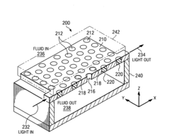
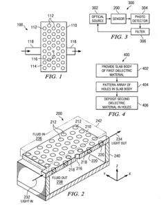
Photonic crystal sensor for small volume sensing
PatentInactiveUS20080089642A1
Innovation
- A two-dimensional photonic crystal slab with a high refractive index dielectric body and a periodic lattice of low refractive index material, such as silicon or GaAs with air-filled holes, is used, incorporating a defect to create a resonance chamber for nanoparticle detection, and 'solid air' materials with a dielectric coefficient of 1.4 or lower are employed to maintain refractive index contrast.
Simulation Techniques
Simulation techniques play a crucial role in the design and optimization of photonic crystal structures for refractive index sensing applications. These computational methods allow researchers to predict and analyze the behavior of light within complex photonic structures, enabling the exploration of various design parameters without the need for costly and time-consuming physical fabrication.
One of the most widely used simulation techniques in photonic crystal design is the Finite-Difference Time-Domain (FDTD) method. FDTD provides a versatile approach for solving Maxwell's equations in the time domain, allowing for the simulation of electromagnetic wave propagation through photonic crystal structures. This method is particularly effective for modeling complex geometries and dispersive materials, making it ideal for studying the intricate interactions between light and photonic crystals.
Another powerful simulation technique is the Plane Wave Expansion (PWE) method, which is primarily used for calculating the band structure and mode profiles of photonic crystals. PWE is particularly useful for determining the photonic band gaps and identifying the frequencies at which light propagation is prohibited within the crystal structure. This information is crucial for designing photonic crystal sensors with high sensitivity and selectivity.
The Finite Element Method (FEM) is also commonly employed in photonic crystal simulations, especially for analyzing the mechanical properties and stress distributions within the structures. FEM is particularly valuable when considering fabrication tolerances and the impact of structural deformations on the optical properties of the photonic crystal.
For more efficient simulations of large-scale photonic crystal structures, researchers often turn to semi-analytical methods such as the Coupled-Mode Theory (CMT) or the Transfer Matrix Method (TMM). These techniques provide a balance between computational efficiency and accuracy, allowing for rapid exploration of design parameters and optimization of sensor performance.
Advanced simulation techniques, such as topology optimization and inverse design algorithms, are increasingly being applied to photonic crystal design. These methods leverage machine learning and artificial intelligence to explore vast design spaces and identify optimal structures that may not be intuitive to human designers.
When simulating photonic crystal sensors for refractive index sensing, it is crucial to accurately model the interaction between the analyte and the photonic crystal structure. This often involves incorporating complex material models and considering the effects of surface functionalization on the optical properties of the sensor.
Simulation techniques also play a vital role in assessing the fabrication tolerances of photonic crystal designs. By introducing controlled variations in the simulated structures, researchers can predict the impact of manufacturing imperfections on sensor performance and develop robust designs that are less sensitive to fabrication errors.
Fabrication Tolerance Analysis
Fabrication tolerance analysis is a critical aspect of photonic crystal design for refractive index sensing applications. The performance of these devices is highly sensitive to structural variations that can occur during the manufacturing process. Understanding and quantifying these tolerances is essential for ensuring the reliability and reproducibility of photonic crystal sensors.
One of the primary challenges in fabrication is maintaining precise control over the geometric parameters of the photonic crystal structure. Even small deviations from the designed dimensions can significantly impact the device's optical properties and sensing capabilities. For instance, variations in the lattice constant, hole diameter, or slab thickness can shift the resonant wavelength and alter the sensitivity of the sensor.
To assess fabrication tolerances, researchers typically employ a combination of simulation and experimental techniques. Finite-difference time-domain (FDTD) simulations are commonly used to model the effects of structural variations on the optical response of the photonic crystal. By systematically varying key parameters within realistic ranges, designers can establish tolerance limits that maintain acceptable sensor performance.
Experimental validation of fabrication tolerances involves the production and characterization of multiple device samples with intentionally varied parameters. This approach provides valuable insights into the real-world impact of manufacturing variations and helps refine simulation models. Advanced fabrication techniques, such as electron-beam lithography and focused ion beam milling, offer high precision but may still introduce nanoscale imperfections that must be accounted for in the tolerance analysis.
The choice of materials and fabrication processes also plays a crucial role in determining tolerance limits. For example, silicon-based photonic crystals may have different fabrication challenges and tolerances compared to those made from III-V semiconductors or polymer materials. Each material system requires tailored fabrication strategies and may exhibit unique sensitivities to process variations.
Optimizing the design for robustness against fabrication variations is an important consideration. This may involve exploring structures that are inherently less sensitive to small geometric changes or incorporating self-correcting features that can compensate for certain types of fabrication errors. Additionally, post-fabrication tuning methods, such as thermal oxidation or selective etching, can be employed to fine-tune device properties and mitigate the effects of fabrication imperfections.
In conclusion, a comprehensive fabrication tolerance analysis is essential for bridging the gap between theoretical design and practical implementation of photonic crystal refractive index sensors. By carefully considering the interplay between design parameters, fabrication limitations, and device performance, researchers can develop more robust and manufacturable sensing platforms.
Unlock deeper insights with Patsnap Eureka Quick Research — get a full tech report to explore trends and direct your research. Try now!
Generate Your Research Report Instantly with AI Agent
Supercharge your innovation with Patsnap Eureka AI Agent Platform!