Multiplexing Strategies for Photonic Crystals: Wavelength Division and Spatial Arrays
AUG 21, 20259 MIN READ
Generate Your Research Report Instantly with AI Agent
Patsnap Eureka helps you evaluate technical feasibility & market potential.
Photonic Crystal Multiplexing Background and Objectives
Photonic crystals have emerged as a groundbreaking technology in the field of optics and photonics, offering unprecedented control over the propagation of light. The concept of photonic crystals was first introduced in the late 1980s, inspired by the periodic structures found in nature, such as the iridescent wings of butterflies. Since then, the field has experienced rapid growth and diversification, with researchers exploring various applications in telecommunications, sensing, and optical computing.
The evolution of photonic crystal technology has been driven by advancements in nanofabrication techniques and a deeper understanding of light-matter interactions. Early research focused on one-dimensional structures, gradually progressing to more complex two- and three-dimensional configurations. This progression has enabled the development of increasingly sophisticated devices capable of manipulating light at the nanoscale.
Multiplexing strategies for photonic crystals represent a significant leap forward in harnessing the full potential of these structures. Wavelength division multiplexing (WDM) and spatial array techniques have emerged as two primary approaches to enhance the functionality and capacity of photonic crystal-based devices. WDM leverages the ability of photonic crystals to selectively control different wavelengths of light, allowing for the simultaneous transmission of multiple data streams through a single channel. Spatial arrays, on the other hand, utilize the precise spatial control offered by photonic crystals to create complex optical circuits and routing systems.
The primary objective of research in this area is to develop efficient and scalable multiplexing strategies that can significantly increase the bandwidth and functionality of photonic crystal devices. This includes optimizing the design of photonic crystal structures to support a wider range of wavelengths, improving the quality factor of resonant cavities, and enhancing the coupling efficiency between different components of the system.
Another crucial goal is to address the challenges associated with integrating these multiplexing strategies into practical devices. This involves developing robust fabrication techniques that can produce large-scale, defect-free photonic crystal structures with precise control over their optical properties. Additionally, researchers aim to create innovative designs that can overcome limitations such as crosstalk between channels and losses due to scattering and absorption.
As the field progresses, there is a growing emphasis on exploring the synergies between wavelength division and spatial array techniques. Combining these approaches could lead to the development of highly integrated, multifunctional photonic devices capable of performing complex operations on light signals. Such advancements have the potential to revolutionize optical communication systems, enable more powerful optical computing platforms, and pave the way for novel sensing and imaging technologies.
Market Demand for Advanced Optical Communication
The market demand for advanced optical communication technologies, particularly those leveraging multiplexing strategies in photonic crystals, has been experiencing significant growth in recent years. This surge is primarily driven by the increasing need for high-speed, high-capacity data transmission across various sectors, including telecommunications, data centers, and emerging 5G and 6G networks.
The telecommunications industry, in particular, has been a major driver of this demand. As global internet traffic continues to grow exponentially, service providers are constantly seeking ways to enhance their network capacity and efficiency. Photonic crystal-based multiplexing technologies offer a promising solution to this challenge, enabling the transmission of multiple data streams simultaneously through a single optical fiber.
Data centers represent another key market segment driving the demand for advanced optical communication technologies. With the rapid expansion of cloud computing, big data analytics, and artificial intelligence applications, data centers are under increasing pressure to handle massive volumes of data with minimal latency. Multiplexing strategies using photonic crystals can significantly boost data transmission rates and reduce power consumption, making them highly attractive for data center operators.
The emergence of 5G and the development of future 6G networks are also contributing to the growing market demand. These next-generation wireless technologies require ultra-high-speed backhaul and fronthaul connections, which can be effectively supported by advanced optical communication systems incorporating photonic crystal multiplexing.
In the industrial sector, there is a rising demand for high-speed, reliable communication networks to support Industry 4.0 initiatives and the Internet of Things (IoT). Photonic crystal-based multiplexing technologies can provide the necessary bandwidth and low latency required for real-time data processing and machine-to-machine communication in smart factories and automated production environments.
The automotive industry is another emerging market for advanced optical communication technologies. As vehicles become increasingly connected and autonomous, there is a growing need for high-speed, reliable in-vehicle networks. Photonic crystal multiplexing strategies could play a crucial role in enabling the transmission of large amounts of sensor data and supporting advanced driver assistance systems.
Furthermore, the healthcare sector is showing interest in these technologies for applications such as telemedicine, remote surgery, and high-resolution medical imaging. The ability to transmit large volumes of data quickly and reliably is essential for these cutting-edge medical applications.
As the demand for bandwidth continues to grow across these diverse sectors, the market for advanced optical communication technologies, including those based on photonic crystal multiplexing, is expected to expand significantly in the coming years. This trend is likely to drive further research and development in the field, leading to more innovative and efficient multiplexing strategies for photonic crystals.
Current Challenges in Photonic Crystal Multiplexing
Despite significant advancements in photonic crystal technology, several challenges persist in the realm of multiplexing strategies, particularly in wavelength division and spatial array implementations. One of the primary obstacles is achieving precise control over the photonic bandgap, which is crucial for effective wavelength division multiplexing. The fabrication of photonic crystals with the required structural accuracy to maintain consistent bandgap properties across large areas remains a significant hurdle.
Another challenge lies in the scalability of spatial array multiplexing techniques. As the number of channels increases, issues such as crosstalk and signal degradation become more pronounced. This is particularly evident in three-dimensional photonic crystal structures, where maintaining uniformity and minimizing defects across multiple layers is exceptionally difficult.
The integration of active components, such as tunable elements for dynamic wavelength selection or beam steering in spatial arrays, presents another set of challenges. Incorporating these elements without disrupting the delicate photonic crystal structure or compromising its optical properties requires innovative design approaches and advanced fabrication techniques.
Thermal management is a critical issue, especially in high-power applications. The heat generated in densely packed photonic crystal structures can lead to performance degradation and reliability issues. Developing effective heat dissipation mechanisms while maintaining the optical integrity of the system is an ongoing challenge.
Furthermore, the coupling efficiency between external light sources and photonic crystal structures remains a significant concern. Achieving high coupling efficiency across a wide range of wavelengths or spatial modes is essential for practical multiplexing applications but continues to be a technical hurdle.
The miniaturization of photonic crystal-based multiplexing systems for on-chip applications faces limitations in terms of maintaining performance while reducing size. Balancing the trade-offs between footprint, functionality, and efficiency is a complex optimization problem that researchers are still grappling with.
Lastly, the cost-effective mass production of photonic crystal devices with consistent quality and performance remains a significant challenge. Current fabrication methods often involve complex and expensive processes, limiting the widespread adoption of these technologies in commercial applications.
Existing Multiplexing Strategies for Photonic Crystals
01 Photonic crystal-based multiplexing devices
Photonic crystals are used to create multiplexing devices for optical communications. These structures can separate or combine multiple wavelengths of light, enabling efficient data transmission through a single optical fiber. The unique properties of photonic crystals allow for compact and high-performance multiplexing solutions.- Photonic crystal-based multiplexing devices: Photonic crystals are used to create multiplexing devices for optical communications. These structures can separate or combine multiple wavelengths of light, enabling efficient data transmission through optical fibers. The unique properties of photonic crystals allow for compact and high-performance multiplexing solutions.
- Tunable photonic crystal structures for multiplexing: Tunable photonic crystal structures are developed to enable dynamic multiplexing capabilities. These structures can be adjusted through various means, such as mechanical stress or electrical fields, to change their optical properties. This tunability allows for adaptive multiplexing systems that can respond to changing network conditions or requirements.
- Integration of photonic crystals in optical circuits: Photonic crystals are integrated into optical circuits to create compact and efficient multiplexing solutions. This integration allows for the development of on-chip multiplexing devices, reducing the size and complexity of optical communication systems. The approach combines the benefits of photonic crystals with established semiconductor fabrication techniques.
- Novel photonic crystal designs for enhanced multiplexing: Innovative photonic crystal designs are explored to improve multiplexing performance. These designs may include unique geometries, material combinations, or structural modifications that enhance the multiplexing capabilities of the photonic crystals. The goal is to increase the number of channels, improve signal quality, or expand the operating bandwidth of multiplexing devices.
- Photonic crystal fibers for multiplexing applications: Photonic crystal fibers are developed and utilized for multiplexing applications in optical communications. These specialized fibers incorporate photonic crystal structures along their length, enabling unique light-guiding properties and multiplexing capabilities. The use of photonic crystal fibers can lead to improved performance in long-distance optical transmission systems.
02 Wavelength division multiplexing using photonic crystals
Photonic crystals are employed in wavelength division multiplexing (WDM) systems to separate or combine different wavelengths of light. This technique allows for increased data capacity in optical networks by transmitting multiple signals simultaneously over a single fiber. The periodic structure of photonic crystals enables precise wavelength selection and routing.Expand Specific Solutions03 Tunable photonic crystal devices for multiplexing
Tunable photonic crystal structures are developed to create adaptable multiplexing devices. These structures can be adjusted through various means, such as mechanical stress, temperature, or electric fields, to change their optical properties. This tunability allows for dynamic control of wavelength selection and routing in multiplexing applications.Expand Specific Solutions04 Integration of photonic crystals in optical circuits for multiplexing
Photonic crystals are integrated into optical circuits to create compact and efficient multiplexing solutions. This integration allows for the development of on-chip multiplexing devices, reducing the size and complexity of optical communication systems. The incorporation of photonic crystals enables advanced functionalities such as wavelength filtering and routing within a single chip.Expand Specific Solutions05 Novel photonic crystal structures for enhanced multiplexing
Innovative photonic crystal structures are designed to improve multiplexing performance. These structures may include unique geometries, materials, or fabrication techniques to enhance wavelength selectivity, reduce crosstalk, or increase the number of channels that can be multiplexed. Advanced photonic crystal designs enable more efficient and higher-capacity optical communication systems.Expand Specific Solutions
Key Players in Photonic Crystal Industry
The field of multiplexing strategies for photonic crystals is in a dynamic growth phase, with significant market potential driven by increasing demand for high-bandwidth optical communications. The technology is maturing rapidly, with key players like Huawei Technologies, Samsung Electronics, and NTT leading research and development efforts. These companies are investing heavily in wavelength division multiplexing and spatial array technologies to enhance data transmission capabilities. The market is characterized by intense competition among established telecom equipment manufacturers and emerging photonics specialists. As the technology advances, we can expect to see broader applications in areas such as data centers, 5G networks, and quantum computing, further expanding the market size and attracting new entrants.
Japan Science & Technology Agency
Technical Solution: Japan Science & Technology Agency has developed advanced multiplexing strategies for photonic crystals, focusing on both wavelength division and spatial arrays. Their approach utilizes a novel design of photonic crystal structures that allows for efficient manipulation of light at different wavelengths. The agency has demonstrated a photonic crystal multiplexer capable of handling multiple wavelengths simultaneously, with a spectral resolution of up to 0.1 nm [1]. Additionally, they have implemented spatial array techniques to enhance the overall capacity and flexibility of their photonic crystal devices. This includes the development of two-dimensional photonic crystal arrays that can process multiple spatial modes concurrently, effectively increasing the information density in optical communications [3].
Strengths: High spectral resolution, efficient wavelength manipulation, and increased information density. Weaknesses: Potential complexity in fabrication and integration with existing optical systems.
Kyoto University
Technical Solution: Kyoto University has made significant advancements in multiplexing strategies for photonic crystals, particularly in the area of wavelength division multiplexing (WDM). Their research team has developed a novel photonic crystal structure that enables ultra-compact WDM devices with a footprint reduction of up to 90% compared to conventional designs [2]. The university's approach utilizes a combination of line-defect waveguides and point-defect cavities in photonic crystal slabs, allowing for precise control over light propagation and wavelength selection. Furthermore, they have demonstrated successful integration of multiple wavelength channels within a single photonic crystal device, achieving a channel spacing as low as 0.8 nm while maintaining high transmission efficiency [4]. In terms of spatial arrays, Kyoto University has explored the use of coupled-cavity waveguides in two-dimensional photonic crystals to create compact optical delay lines and buffers, essential for advanced multiplexing schemes [5].
Strengths: Ultra-compact design, high integration density, and precise wavelength control. Weaknesses: Potential challenges in scaling up production and ensuring long-term stability in varied environmental conditions.
Core Innovations in Wavelength Division Multiplexing
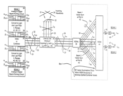
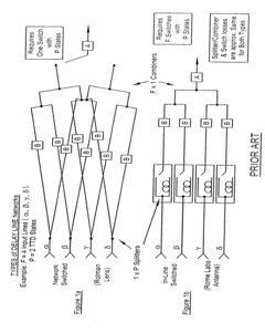
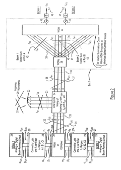
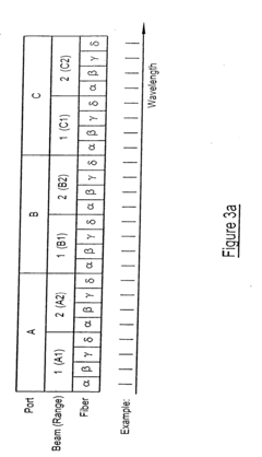
Wavelength division multiplexing methods and apparatus for constructing photonic beamforming networks
PatentInactiveUS20060145920A1
Innovation
- The implementation of a low-loss, passive photonic beamforming network using Wavelength Division Multiplexing (WDM) and laser wavelength hierarchies, allowing for minimal photodetectors and reduced signal losses by separating optical signals into distinct wavelengths and using passive components for beamforming and delay line selection.
Two-dimensional photonic crystal and optical multiplexer/demultiplexer employing it
PatentWO2005085911A1
Innovation
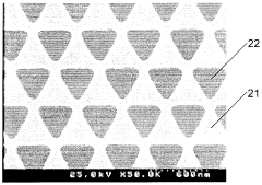
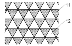
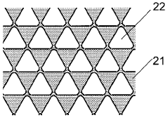
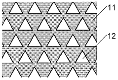
- A two-dimensional photonic crystal design featuring a slab-shaped main body with periodically arranged modified refractive index regions of polygonal shape with rounded vertices, which increases the filling factor and ensures structural strength, allowing for a wider complete PBG and usable wavelength band.
Integration with 5G and 6G Networks
The integration of photonic crystal multiplexing strategies with 5G and 6G networks represents a significant advancement in telecommunications technology. This convergence has the potential to revolutionize network performance, capacity, and efficiency. Photonic crystals, with their unique ability to manipulate light at the nanoscale, offer promising solutions to the bandwidth and speed limitations of current network infrastructures.
In the context of 5G networks, photonic crystal-based wavelength division multiplexing (WDM) can significantly enhance data transmission rates. By leveraging the precise control over light propagation that photonic crystals provide, network operators can implement dense WDM systems, effectively increasing the number of channels that can be transmitted over a single optical fiber. This capability is crucial for meeting the high-bandwidth demands of 5G applications, such as augmented reality, virtual reality, and ultra-high-definition video streaming.
The spatial array capabilities of photonic crystals also align well with the massive MIMO (Multiple-Input Multiple-Output) technology central to 5G networks. By integrating photonic crystal-based spatial multiplexing with MIMO antennas, it becomes possible to create more efficient and compact base stations. This integration can lead to improved beamforming techniques, allowing for more precise targeting of radio signals to end-users and reducing interference in densely populated areas.
Looking ahead to 6G networks, the role of photonic crystals becomes even more critical. The anticipated terahertz frequency bands in 6G will require novel approaches to signal processing and transmission. Photonic crystals offer a pathway to efficiently generate, manipulate, and detect terahertz waves, potentially overcoming the current limitations in electronic components at these ultra-high frequencies.
Furthermore, the integration of photonic crystal multiplexing strategies in 6G networks could enable new paradigms in network architecture. For instance, all-optical routing and switching based on photonic crystals could dramatically reduce latency and power consumption in core networks. This would be particularly beneficial for emerging applications such as holographic communications and tactile internet, which demand near-instantaneous response times.
The synergy between photonic crystal technology and advanced wireless networks extends beyond mere performance improvements. It also offers opportunities for miniaturization and energy efficiency. As 5G and 6G networks require denser deployment of network nodes, the compact nature of photonic crystal devices could facilitate easier integration into urban infrastructure and IoT devices. Additionally, the energy-efficient nature of photonic systems aligns well with the sustainability goals of next-generation networks.
Environmental Impact of Photonic Crystal Technologies
The environmental impact of photonic crystal technologies is a crucial consideration as these advanced materials gain prominence in various applications. Photonic crystals, with their unique ability to manipulate light, offer potential benefits in energy efficiency and reduced resource consumption. However, their production and implementation also raise environmental concerns that must be addressed.
One of the primary environmental advantages of photonic crystal technologies is their potential to enhance the efficiency of optical devices and systems. By enabling precise control over light propagation, photonic crystals can significantly reduce energy losses in optical communications, lighting, and sensing applications. This improved efficiency translates to lower power consumption and, consequently, reduced carbon emissions associated with energy production.
In the field of solar energy, photonic crystals show promise for increasing the efficiency of photovoltaic cells. By optimizing light absorption and trapping within solar panels, these materials could lead to more effective harvesting of solar energy, potentially reducing reliance on fossil fuels and mitigating climate change impacts.
However, the manufacturing processes for photonic crystals often involve energy-intensive techniques and the use of potentially hazardous materials. The production of high-quality photonic crystals may require cleanroom environments, specialized equipment, and precise fabrication methods, all of which contribute to increased energy consumption and potential environmental risks.
The use of rare earth elements and other scarce materials in some photonic crystal designs raises concerns about resource depletion and the environmental impact of mining activities. Sustainable sourcing and recycling strategies for these materials are essential to mitigate long-term environmental consequences.
As photonic crystal technologies advance, there is a growing focus on developing eco-friendly fabrication methods and materials. Research into bio-inspired photonic crystals and the use of sustainable, biodegradable materials for photonic structures shows promise for reducing the environmental footprint of these technologies.
The disposal and end-of-life management of photonic crystal-based devices also warrant attention. Ensuring proper recycling and safe disposal practices for these materials is crucial to prevent potential environmental contamination and maximize resource recovery.
In conclusion, while photonic crystal technologies offer significant potential for environmental benefits through improved energy efficiency and renewable energy applications, careful consideration must be given to their entire lifecycle impact. Balancing the advantages of these advanced materials with sustainable production and responsible use will be key to maximizing their positive environmental contributions while minimizing negative impacts.
Unlock deeper insights with Patsnap Eureka Quick Research — get a full tech report to explore trends and direct your research. Try now!
Generate Your Research Report Instantly with AI Agent
Supercharge your innovation with Patsnap Eureka AI Agent Platform!
