

Memristive Devices as High-Density Artificial Synapses.
SEP 2, 202510 MIN READ
Generate Your Research Report Instantly with AI Agent
Patsnap Eureka helps you evaluate technical feasibility & market potential.
Memristive Technology Background and Objectives
Memristive devices have emerged as a revolutionary technology in the field of neuromorphic computing, representing a significant departure from traditional von Neumann architecture. First theorized by Leon Chua in 1971, memristors (memory resistors) remained largely theoretical until 2008 when researchers at HP Labs demonstrated the first physical implementation. This breakthrough catalyzed extensive research into memristive technologies as potential building blocks for brain-inspired computing systems.
The evolution of memristive technology has been driven by the increasing limitations of conventional computing architectures when handling complex cognitive tasks and the exponential growth in data processing requirements. Traditional computing systems face fundamental bottlenecks in energy efficiency and processing speed due to the physical separation between memory and processing units. Memristive devices offer a promising solution by integrating memory and computation functions within the same physical structure.
As artificial synapses, memristive devices can emulate the fundamental properties of biological synapses, including plasticity, analog weight modulation, and non-volatile memory characteristics. These properties enable the implementation of learning algorithms directly in hardware, potentially reducing energy consumption by several orders of magnitude compared to software implementations on conventional hardware.
The current technological trajectory is focused on developing memristive devices with improved reliability, endurance, and scalability. Various material systems are being explored, including metal oxides (HfOx, TaOx), phase-change materials, and ferroelectric materials, each offering distinct advantages in terms of switching characteristics, retention, and integration potential with CMOS technology.
The primary technical objectives in this field include achieving higher device density to enable large-scale neural networks, enhancing the precision and stability of synaptic weight states, reducing energy consumption per synaptic operation, and developing fabrication processes compatible with existing semiconductor manufacturing infrastructure.
Another critical goal is to bridge the gap between device-level characteristics and system-level performance by developing appropriate neural network architectures and training algorithms specifically optimized for memristive hardware. This includes addressing challenges related to device variability, non-ideal switching behavior, and limited precision.
Looking forward, the field aims to demonstrate practical applications of memristive neural networks in edge computing, autonomous systems, and data centers, where energy efficiency and real-time processing of unstructured data are paramount. The ultimate vision is to create neuromorphic systems that approach the energy efficiency and cognitive capabilities of biological brains while maintaining the programmability and precision of digital computers.
Market Analysis for Neuromorphic Computing Solutions
The neuromorphic computing market is experiencing significant growth, driven by the increasing demand for AI applications that require efficient processing of complex neural networks. Current market size estimates place the global neuromorphic computing sector at approximately $2.5 billion in 2023, with projections indicating a compound annual growth rate of 20-25% over the next five years. This growth trajectory is supported by substantial investments from both private and public sectors, with government initiatives in the US, EU, and China allocating dedicated funding for neuromorphic research and development.
Market segmentation reveals distinct application areas driving demand for memristive-based neuromorphic solutions. The largest current segment is data centers and cloud computing, where energy efficiency and processing speed are critical factors. Healthcare applications represent the fastest-growing segment, with neuromorphic systems showing promise in medical imaging analysis, drug discovery, and personalized medicine. Autonomous vehicles and advanced robotics form another significant market segment, requiring real-time processing capabilities that conventional computing struggles to deliver efficiently.
Customer needs analysis indicates that power efficiency remains the primary concern across all market segments. Traditional von Neumann architecture-based systems consume excessive energy when implementing neural network operations, creating a clear market opportunity for memristive device solutions that can reduce power consumption by orders of magnitude. Performance density is another critical market driver, with customers seeking solutions that can process increasingly complex AI models within constrained physical spaces and thermal envelopes.
Competitive landscape assessment shows that while established semiconductor companies like Intel, IBM, and Samsung have made significant investments in neuromorphic technology, numerous specialized startups focused exclusively on memristive solutions have emerged. These include BrainChip, Mythic, and SynSense, each developing proprietary approaches to memristive-based neural processing. This fragmented market indicates both significant opportunity and competitive pressure for new entrants.
Market barriers include manufacturing scalability challenges, with current fabrication processes for memristive devices still facing yield and consistency issues at commercial scales. Integration with existing software ecosystems represents another significant barrier, as the adoption of neuromorphic solutions requires substantial adaptation of existing AI frameworks and development tools. These barriers are reflected in the current pricing models, which remain significantly higher than conventional computing solutions on a per-unit basis, though the total cost of ownership calculations increasingly favor neuromorphic approaches when energy consumption is factored in.
Current State and Challenges in Memristive Device Development
Memristive devices have emerged as promising candidates for implementing artificial synapses in neuromorphic computing systems due to their ability to mimic biological synaptic functions. Currently, various types of memristive devices are being explored, including resistive random-access memory (RRAM), phase-change memory (PCM), ferroelectric RAM (FeRAM), and magnetic RAM (MRAM). Each technology offers unique advantages in terms of switching speed, energy consumption, endurance, and integration density.
The global research landscape shows significant activity in memristive device development across North America, Europe, and Asia. Leading research institutions such as HP Labs, IBM Research, Stanford University, MIT, and Chinese Academy of Sciences have made substantial contributions to advancing memristive technologies. In the industrial sector, companies like Intel, Samsung, SK Hynix, and Micron are actively pursuing memristive solutions for next-generation memory and computing applications.
Despite promising progress, several critical challenges impede the widespread adoption of memristive devices as artificial synapses. Device variability remains a significant concern, with cycle-to-cycle and device-to-device variations affecting reliability and predictability. These variations stem from stochastic processes during switching operations and manufacturing inconsistencies, making it difficult to achieve uniform performance across large arrays.
Endurance limitations present another major hurdle. While biological synapses can undergo modifications billions of times, current memristive devices typically exhibit endurance in the range of 10^6 to 10^9 cycles, which falls short for long-term operation in neuromorphic systems. Material degradation and structural changes during repeated switching operations contribute to this limitation.
The trade-off between retention and switching speed poses a fundamental challenge. Devices with excellent non-volatility often require higher energy for switching, while easily switchable devices may suffer from poor data retention. This dichotomy complicates the design of energy-efficient neuromorphic systems that require both fast operation and long-term memory storage.
Scaling issues also persist as researchers attempt to increase integration density. As device dimensions shrink below 10nm, quantum effects and thermal instabilities become more pronounced, affecting device reliability and performance. Additionally, the complex materials and structures used in advanced memristive devices present integration challenges with conventional CMOS technology.
The implementation of precise analog states, essential for mimicking the continuous weight changes in biological synapses, remains technically challenging. Most current devices exhibit discrete resistance states rather than truly continuous modulation capabilities, limiting their ability to accurately represent synaptic weights in neural networks.
Current Memristive Implementation Approaches
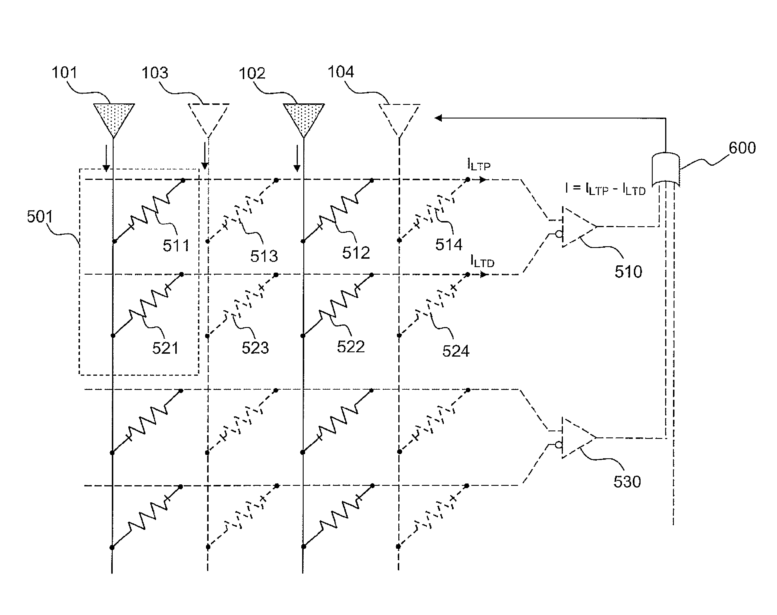
01 High-density memristor array architectures
High-density memristor arrays can be achieved through specific architectural designs that optimize space utilization and connectivity. These architectures include crossbar arrays where memristive devices are positioned at the intersection of perpendicular conductive lines, allowing for maximum device density. Advanced 3D stacking techniques further increase density by building multiple layers of memristive elements. These architectural approaches enable the creation of ultra-high-density memory and neuromorphic computing systems while minimizing the footprint of the overall device.- Crossbar array architectures for high-density memristive devices: Crossbar array architectures enable high-density integration of memristive devices by arranging them at the intersection of perpendicular word and bit lines. This configuration maximizes device density while minimizing the footprint of the memory array. The architecture allows for efficient addressing of individual memristors and supports parallel operations, making it suitable for high-performance computing applications. Advanced crossbar designs incorporate selector devices to mitigate sneak path currents and improve read/write reliability in high-density arrays.
- Materials and fabrication techniques for high-density memristive devices: Various materials and fabrication techniques are employed to create high-density memristive devices. Metal oxides such as HfOx, TiOx, and TaOx are commonly used as switching layers due to their excellent scaling properties and compatibility with CMOS processes. Advanced deposition methods including atomic layer deposition (ALD) and physical vapor deposition (PVD) enable precise control of layer thickness at nanometer scales. 3D stacking and vertical integration techniques further increase memory density by utilizing the vertical dimension, allowing multiple layers of memristive devices to be fabricated on top of each other.
- Neuromorphic computing applications using high-density memristive arrays: High-density memristive device arrays are particularly suitable for neuromorphic computing applications due to their ability to mimic synaptic behavior. These arrays can implement artificial neural networks with high connectivity and efficiency, enabling complex pattern recognition and machine learning tasks. The analog nature of memristive devices allows them to store multiple states, representing synaptic weights in neural networks. This capability, combined with their high density, enables the implementation of large-scale neural networks with significantly reduced power consumption compared to conventional computing architectures.
- Circuit design and integration for high-density memristive systems: Specialized circuit designs are essential for effectively integrating high-density memristive devices into functional systems. These include sense amplifiers optimized for detecting the resistance states of memristors, write drivers capable of providing precise programming pulses, and addressing circuits for selecting specific devices within large arrays. Advanced integration schemes incorporate peripheral CMOS circuitry with memristive arrays to create complete memory or computing systems. Novel circuit techniques also address challenges such as variability compensation, error correction, and power management that are critical for reliable operation of high-density memristive systems.
- Scaling and reliability solutions for high-density memristive technologies: As memristive devices scale to higher densities, several challenges related to reliability and performance must be addressed. These include resistance drift, endurance limitations, and device-to-device variability. Solutions involve developing specialized programming algorithms that adapt to changing device characteristics, implementing error correction codes, and designing redundancy schemes. Advanced selector devices are integrated with memristors to prevent sneak path currents in high-density arrays. Novel materials and interface engineering techniques improve retention time and cycling endurance, which are critical for commercial viability of high-density memristive technologies.
02 Materials and fabrication techniques for high-density memristive devices
Novel materials and fabrication techniques are crucial for creating high-density memristive devices. These include the use of specialized metal oxides, phase-change materials, and other resistive switching materials that can be deposited in thin films. Advanced nanofabrication methods such as atomic layer deposition, electron beam lithography, and self-assembly techniques enable the creation of nanoscale memristive elements. These approaches allow for the miniaturization of individual memristors while maintaining their electrical characteristics, which is essential for high-density integration.Expand Specific Solutions03 Neuromorphic computing applications of high-density memristive devices
High-density memristive devices are particularly valuable for neuromorphic computing applications, where they can mimic the functionality of biological synapses and neurons. These devices can be arranged in dense networks to implement artificial neural networks directly in hardware, offering significant advantages in terms of energy efficiency and processing speed compared to conventional computing architectures. The ability to pack numerous memristive elements in a small area enables the creation of brain-inspired computing systems with high levels of connectivity and parallelism.Expand Specific Solutions04 Circuit design and signal processing for high-density memristive systems
Specialized circuit designs and signal processing techniques are required to effectively utilize high-density memristive devices. These include sensing circuits capable of accurately reading the resistance states of closely packed memristors, addressing schemes to select specific devices within dense arrays, and programming circuits that can precisely control the resistance states. Advanced error correction and noise reduction techniques are also essential to maintain data integrity in high-density configurations where interference between adjacent devices can be significant.Expand Specific Solutions05 Integration of high-density memristive devices with CMOS technology
The integration of high-density memristive devices with conventional CMOS technology is critical for practical applications. This integration involves developing compatible fabrication processes, addressing interface issues between memristive materials and silicon, and designing hybrid circuits that leverage the strengths of both technologies. Back-end-of-line integration approaches allow memristive devices to be fabricated above the CMOS layer, maximizing density while maintaining manufacturability. This hybrid approach enables the creation of high-performance computing systems that combine the logic capabilities of CMOS with the memory and adaptive features of memristors.Expand Specific Solutions
Key Industry Players in Memristive Device Manufacturing
The memristive devices market for artificial synapses is currently in an early growth phase, characterized by intensive R&D activities and emerging commercial applications. The global market is projected to expand significantly as neuromorphic computing gains traction, with estimates suggesting a multi-billion dollar opportunity by 2030. Technologically, the field shows varying maturity levels across players. HP Enterprise and IBM lead with foundational patents and commercial prototypes, while academic institutions like Huazhong University and Nanjing University contribute significant fundamental research. Micron and SK Hynix are leveraging their semiconductor expertise to develop scalable manufacturing processes. Qualcomm is focusing on mobile applications, while research organizations like Fraunhofer and KIST are bridging the gap between laboratory demonstrations and industrial implementation through collaborative innovation ecosystems.
Hewlett Packard Enterprise Development LP
Technical Solution: Hewlett Packard Enterprise (HPE) has pioneered memristive technology as artificial synapses through their memristor crossbar architecture. Their approach utilizes metal-oxide memristors arranged in dense crossbar arrays that can achieve synapse-like behavior with analog conductance states. HPE's memristive devices implement spike-timing-dependent plasticity (STDP) learning rules directly in hardware, enabling efficient neuromorphic computing. Their technology demonstrates high integration density (>10^10 devices/cm²) and low power consumption (<10 pJ per synaptic operation). HPE has developed specialized materials engineering techniques to control oxygen vacancy movement within metal oxides like TiO₂ and HfO₂, allowing precise tuning of resistance states. Their crossbar architecture enables massively parallel vector-matrix multiplication operations essential for neural network acceleration[1][3].
Strengths: Industry-leading integration density and pioneering position in memristor technology with mature fabrication processes. Their crossbar architecture enables true in-memory computing, eliminating the von Neumann bottleneck. Weaknesses: Challenges with device variability and retention time limitations in certain environmental conditions, requiring additional compensation circuitry that increases overall system complexity.
International Business Machines Corp.
Technical Solution: IBM has developed phase-change memory (PCM) based memristive devices for neuromorphic applications, focusing on multi-level resistance states to mimic biological synapses. Their technology utilizes chalcogenide materials (primarily Ge₂Sb₂Te₅) that undergo phase transitions between crystalline and amorphous states when subjected to electrical pulses. IBM's approach enables approximately 8-bit precision per synapse with their advanced programming algorithms. Their PCM devices demonstrate excellent endurance (>10⁷ cycles) and retention characteristics (>10 years at 85°C). IBM has integrated these memristive synapses with CMOS neurons in their TrueNorth and subsequent neuromorphic architectures. They've demonstrated on-chip learning capabilities through their array-level implementation of backpropagation algorithms, achieving significant energy efficiency improvements compared to conventional computing approaches. IBM has also pioneered the use of stochastic computing techniques with memristive devices to implement probabilistic neural networks[2][5].
Strengths: Superior endurance characteristics and established manufacturing compatibility with CMOS processes. IBM's multi-bit precision capability enables higher accuracy in neural network implementations. Weaknesses: Phase-change materials require relatively high programming currents compared to other memristive technologies, and their switching speed is limited by crystallization dynamics, creating challenges for ultra-high-speed applications.
Core Patents and Breakthroughs in Memristive Synapse Design
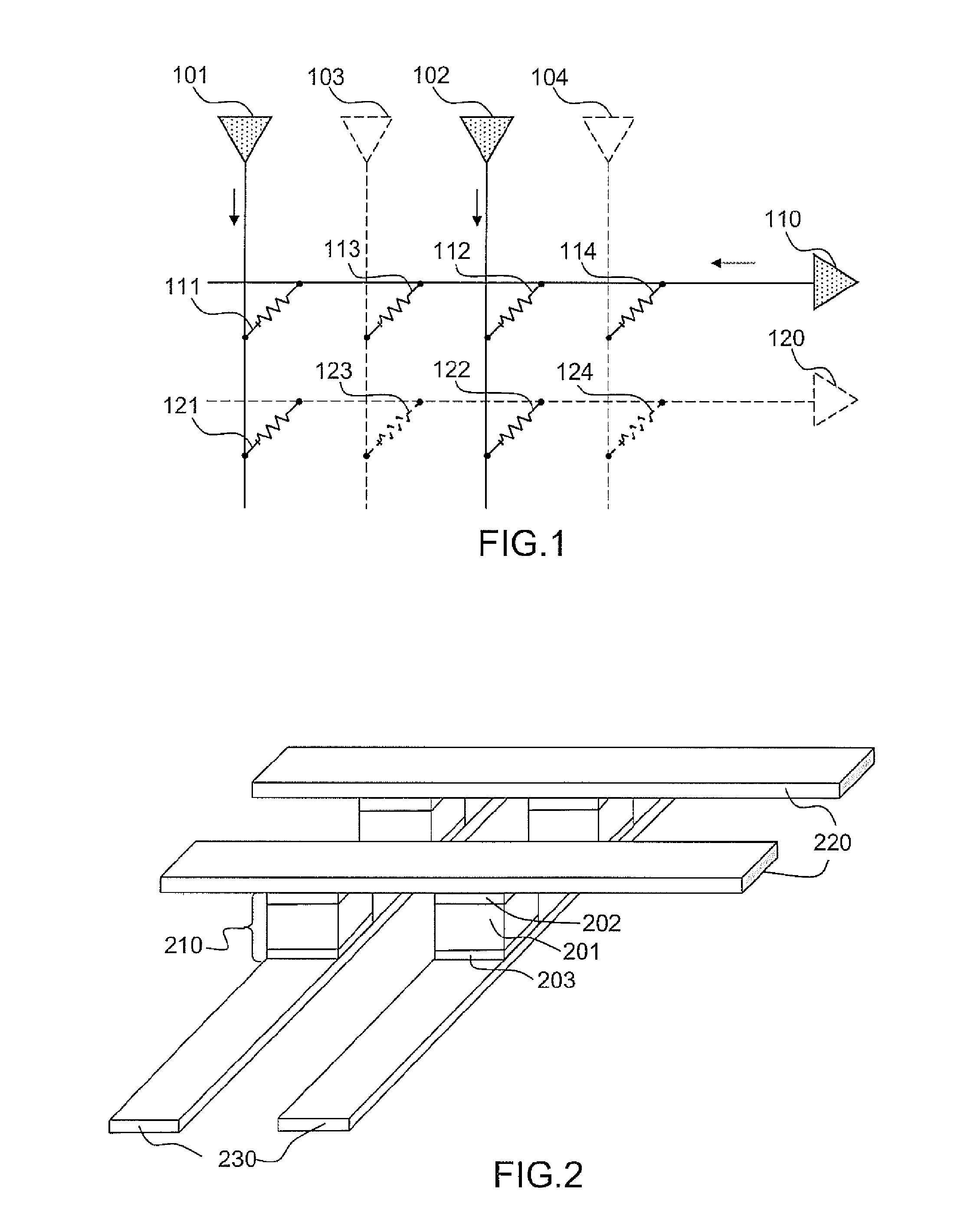
Network of artificial neurons based on complementary memristive devices
PatentActiveUS9396431B2
Innovation
- A neural network architecture utilizing two memristive devices in opposition to form an artificial synapse, allowing for both increasing and decreasing conductance based on the state of connected neurons, with specific pulse configurations and thresholds to achieve alternating conductance variations.
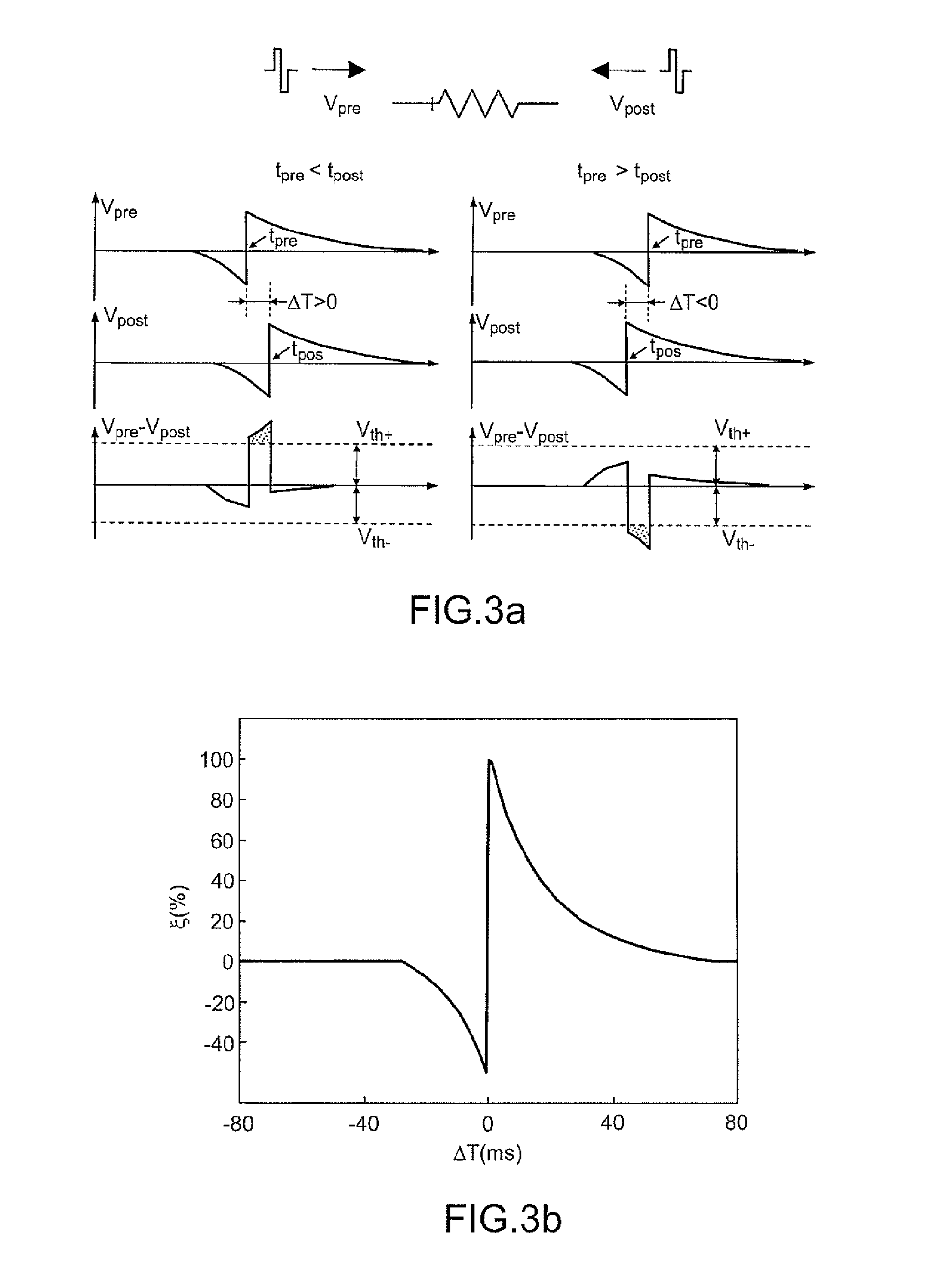

Method and Means for Operating a Complementary Analogue Reconfigurable Memristive Resistive Switch and Use Thereof as an Artificial Synapse
PatentActiveUS20190122730A1
Innovation
- A memristive device with a BFTO/BFO/BFTO three-ply layer and titanium traps, allowing for flexible, complementary adjustment of potential barriers through voltage pulses, enabling the implementation of fuzzy logic and all four learning curves.


Energy Efficiency Considerations in Neuromorphic Hardware
Energy efficiency represents a critical factor in the development and implementation of neuromorphic hardware systems utilizing memristive devices as artificial synapses. Traditional von Neumann computing architectures face significant energy constraints when simulating neural networks, primarily due to the energy-intensive data transfer between memory and processing units. Memristive devices offer a promising solution by integrating memory and computation within the same physical structure, substantially reducing energy consumption associated with data movement.
The power efficiency of memristive-based neuromorphic systems stems from their ability to perform computations with minimal energy expenditure. Current research indicates that memristive synapses can achieve energy consumption as low as femtojoules per synaptic operation, representing orders of magnitude improvement over conventional CMOS implementations. This efficiency derives from the fundamental operating principles of memristive devices, which can maintain their state without continuous power supply, enabling persistent memory with negligible static power consumption.
Thermal management presents another crucial consideration in high-density memristive arrays. As device density increases, heat dissipation becomes a significant challenge that can affect both performance and reliability. Advanced cooling strategies and thermally-aware circuit designs are being developed to address these concerns, including the implementation of thermal buffers and optimized pulse schemes that minimize heat generation during switching operations.
Scaling considerations further impact energy efficiency in memristive neuromorphic systems. As device dimensions shrink, leakage currents and parasitic effects can compromise energy performance. Research indicates that careful material selection and device engineering can mitigate these issues, with emerging two-dimensional materials and novel oxide compositions showing particular promise for maintaining energy efficiency at nanoscale dimensions.
Power management techniques specific to memristive neuromorphic hardware are evolving rapidly. These include adaptive power gating, variable precision computation, and activity-dependent energy allocation strategies. Such approaches enable dynamic adjustment of energy consumption based on computational demands, optimizing efficiency across diverse workloads and operating conditions.
The integration of memristive devices with ultra-low-power CMOS circuits represents another frontier in energy-efficient neuromorphic computing. Hybrid designs that leverage the strengths of both technologies can achieve superior energy performance while maintaining computational flexibility. Recent demonstrations have shown that such hybrid systems can achieve energy efficiencies approaching the theoretical limits of neuromorphic computation.
Reliability and Endurance of Memristive Synaptic Arrays
Reliability and endurance represent critical performance metrics for memristive synaptic arrays in neuromorphic computing applications. Current memristive devices face significant challenges in maintaining consistent performance over extended operational periods, with most commercial-grade devices demonstrating endurance levels between 10^6 to 10^9 switching cycles. This falls short of the requirements for large-scale neural network implementations, which may demand 10^12 or more cycles for continuous learning applications.
The reliability issues in memristive synaptic arrays stem from several fundamental mechanisms. Atomic migration and structural changes within the switching material lead to gradual degradation of the conductive filament, resulting in resistance drift over time. This phenomenon manifests as weight instability in artificial neural networks, compromising computational accuracy. Additionally, thermal effects during repeated switching operations accelerate material fatigue, particularly at the interface between the active layer and electrodes.
Environmental factors further compound these challenges, with humidity and temperature fluctuations significantly impacting device performance. Research by IBM and Stanford University has demonstrated that controlling operational temperature within ±5°C can extend device lifetime by up to 40%, highlighting the importance of environmental stability in deployment scenarios.
Recent advances in material engineering have yielded promising improvements in endurance characteristics. Hafnium oxide-based memristors with engineered oxygen vacancy distributions have demonstrated enhanced cycle stability, achieving up to 10^10 switching operations while maintaining a resistance ratio above 10. Similarly, tantalum oxide devices with gradient doping profiles exhibit improved retention characteristics, maintaining state fidelity for over 10 years at room temperature.
Statistical analysis of large memristive arrays reveals significant device-to-device variability, with resistance states following log-normal distributions that widen with increased cycling. This variability necessitates robust error correction mechanisms and redundancy strategies in practical implementations. Techniques such as write-verify-write protocols and adaptive programming schemes have been developed to mitigate these effects, though they introduce additional complexity and energy overhead.
Accelerated aging tests provide valuable insights into long-term reliability, with most current devices showing acceptable performance degradation (less than 20% drift) over projected 10-year lifespans under normal operating conditions. However, these projections typically assume ideal usage patterns and may not fully account for the complex workloads encountered in continuous learning scenarios.
The trade-off between endurance and other performance metrics presents another significant challenge. Devices optimized for high endurance often sacrifice switching speed or energy efficiency, necessitating careful system-level design considerations. Future research directions must focus on developing comprehensive reliability models that account for these interdependencies and guide material optimization efforts.
Unlock deeper insights with Patsnap Eureka Quick Research — get a full tech report to explore trends and direct your research. Try now!
Generate Your Research Report Instantly with AI Agent
Supercharge your innovation with Patsnap Eureka AI Agent Platform!