Microcomb Coherence Control In Multi-Chip Photonic Systems
AUG 29, 202510 MIN READ
Generate Your Research Report Instantly with AI Agent
Patsnap Eureka helps you evaluate technical feasibility & market potential.
Microcomb Technology Evolution and Objectives
Microcombs, or optical frequency combs generated in microresonators, have emerged as a revolutionary technology in integrated photonics over the past two decades. The evolution of this technology began with the fundamental discovery of optical Kerr frequency combs in microresonators in the early 2000s, marking a significant departure from traditional mode-locked laser-based frequency combs. This miniaturization breakthrough enabled the integration of frequency comb sources onto photonic chips, dramatically reducing size, power consumption, and potentially cost.
The technological trajectory of microcombs has been characterized by several distinct phases. Initially, researchers focused on demonstrating basic comb generation in various material platforms including silica, silicon nitride, and lithium niobate. The second phase, occurring roughly between 2010-2015, centered on understanding the complex nonlinear dynamics governing microcomb formation, particularly the critical transition from chaotic states to coherent soliton states.
A pivotal advancement came with the reliable generation of dissipative Kerr solitons (DKS) around 2014, which provided a pathway to fully coherent microcombs with predictable spectral envelopes. This breakthrough accelerated applications development and industry interest, as coherent microcombs became viable for practical systems.
The current technological frontier, beginning around 2018, focuses on multi-chip integration challenges, where maintaining coherence across chip boundaries represents a fundamental obstacle. Coherence control mechanisms have evolved from simple thermal tuning to sophisticated feedback systems incorporating phase-locked loops and advanced modulation techniques.
The objectives of current microcomb research in multi-chip photonic systems are multifaceted. Primary goals include achieving robust coherence preservation during chip-to-chip light transfer, developing standardized interfaces for heterogeneous integration, and creating scalable architectures that maintain phase stability across multiple interconnected photonic chips.
Technical targets specifically focus on reducing phase noise below -140 dBc/Hz at 10 kHz offset, maintaining coherence times exceeding 100 milliseconds in multi-chip environments, and developing control systems capable of compensating for thermal and mechanical perturbations with response times under 1 microsecond.
Long-term objectives extend to creating fully programmable multi-chip photonic systems where microcombs serve as coherent light sources for applications including optical computing, quantum information processing, and ultra-high-capacity telecommunications. The ultimate vision encompasses self-stabilizing microcomb networks that can maintain coherence autonomously across complex photonic circuits, potentially revolutionizing fields from precision metrology to integrated quantum photonics.
Market Applications for Integrated Photonic Systems
Integrated photonic systems incorporating microcombs are revolutionizing multiple high-value markets through their unique capabilities in signal processing, sensing, and communications. The telecommunications sector represents the most immediate and substantial market opportunity, with data centers and network infrastructure providers actively seeking solutions that can handle exponentially growing bandwidth demands while reducing power consumption. Microcomb-based wavelength division multiplexing (WDM) systems offer data transmission rates exceeding 100 Tbps through a single optical fiber, addressing critical bottlenecks in modern telecommunications infrastructure.
The rapidly expanding LiDAR market, projected to reach significant growth in autonomous vehicle applications, stands to benefit tremendously from coherent microcomb technology. Current LiDAR systems suffer from limitations in range, resolution, and cost-effectiveness that integrated photonic solutions directly address. By enabling frequency-modulated continuous-wave (FMCW) LiDAR with unprecedented coherence properties, these systems can achieve superior distance measurement precision while maintaining compact form factors essential for vehicle integration.
Quantum computing represents another frontier market where integrated photonic systems with controlled microcomb coherence offer transformative potential. As quantum information processing advances beyond laboratory demonstrations toward practical computing platforms, the need for scalable photonic interconnects and quantum state manipulation becomes critical. Microcomb-based quantum photonic processors provide the necessary quantum state generation, manipulation, and measurement capabilities within a chip-scale platform compatible with existing semiconductor manufacturing processes.
The biomedical sensing and imaging market presents significant opportunities for microcomb technology, particularly in optical coherence tomography (OCT) and spectroscopic applications. The exceptional spectral purity and broad bandwidth of microcombs enable unprecedented resolution in tissue imaging and molecular detection. Healthcare providers increasingly demand portable, high-performance diagnostic tools that can operate in point-of-care settings, creating a growing market for integrated photonic solutions.
Aerospace and defense applications constitute a specialized but lucrative market segment for coherent microcomb technology. Advanced radar systems, secure communications networks, and precision navigation tools all benefit from the unique spectral properties and compact form factor of integrated photonic systems. Military and space applications place premium value on size, weight, power, and cost (SWaP-C) advantages that multi-chip photonic integration delivers.
The emerging neuromorphic computing market represents perhaps the most forward-looking application area. As artificial intelligence systems continue their exponential growth in complexity and deployment, the limitations of electronic computing architectures become increasingly apparent. Photonic neural networks leveraging coherent microcombs offer orders-of-magnitude improvements in processing speed and energy efficiency for specific AI workloads, positioning them as critical enabling technologies for next-generation computing paradigms.
Coherence Control Challenges in Multi-Chip Integration
Multi-chip photonic integration presents significant coherence control challenges that must be addressed to realize the full potential of microcomb technology. The primary obstacle lies in maintaining phase coherence across multiple chips, as even minor variations in temperature, mechanical stress, or fabrication tolerances can disrupt the delicate phase relationships essential for proper system operation. These variations introduce unpredictable phase shifts that compromise the integrity of optical signals traversing chip boundaries.
The thermal management challenge is particularly acute in multi-chip configurations. Each photonic chip generates heat differently based on its specific components and operational parameters. Without precise thermal control mechanisms, temperature gradients emerge between chips, causing differential thermal expansion and refractive index changes that directly impact optical path lengths and phase relationships. These thermal fluctuations occur at various timescales, from rapid transients to slow drifts, requiring multi-tiered compensation strategies.
Mechanical coupling issues further complicate coherence maintenance. Chip-to-chip interfaces are susceptible to vibrations and mechanical stresses that can dynamically alter optical coupling efficiency and phase. Even nanometer-scale displacements at these interfaces can significantly degrade system performance, necessitating advanced packaging solutions that provide both mechanical stability and thermal isolation.
The fundamental challenge of clock distribution across multiple chips remains largely unsolved in current implementations. Synchronizing optical and electronic clocks across chip boundaries with femtosecond precision requires novel approaches that go beyond conventional electronic solutions. The propagation delays and jitter accumulation between chips create timing uncertainties that directly translate to phase noise in the optical domain.
Fabrication variations between chips present another layer of complexity. Despite advances in manufacturing precision, chip-to-chip variations in waveguide dimensions, material properties, and resonator characteristics are inevitable. These variations result in mismatched dispersion profiles and resonance conditions that must be actively compensated to maintain coherent operation across the system.
Environmental sensitivity compounds these challenges, as external perturbations affect each chip differently based on its position within the system and its specific design characteristics. Acoustic vibrations, air currents, and electromagnetic interference can all induce phase fluctuations that are difficult to predict and mitigate, particularly in field-deployed systems outside controlled laboratory environments.
Addressing these coherence control challenges requires an integrated approach combining innovations in chip design, packaging technology, control systems, and calibration methodologies. The development of robust solutions will be critical for scaling microcomb technology to complex multi-chip architectures capable of supporting advanced applications in communications, sensing, and quantum information processing.
Current Coherence Control Methodologies
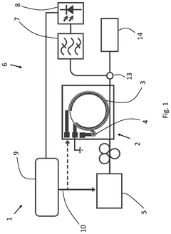
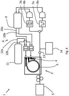
01 Optical microcomb generation and stabilization
Optical microcombs are generated using microresonators that convert continuous-wave laser light into coherent frequency combs. The coherence of these microcombs can be enhanced through various stabilization techniques, including phase-locking, thermal control, and pump laser optimization. These methods ensure stable operation and high coherence across the generated comb lines, which is essential for applications requiring precise frequency references.- Generation and stabilization of microcomb coherence: Techniques for generating and stabilizing coherent microcombs involve controlling the optical resonator conditions and pump laser parameters. Methods include precise thermal management, dispersion engineering, and feedback mechanisms to maintain phase coherence across the comb lines. These approaches enable the production of stable, low-noise frequency combs with predictable spectral characteristics, which is essential for high-precision applications.
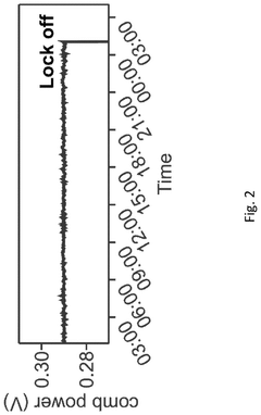
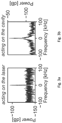
- Microcomb coherence measurement and characterization: Systems and methods for measuring and characterizing the coherence properties of microcombs involve specialized interferometric techniques and spectral analysis. These approaches enable the quantification of phase noise, coherence time, and spectral purity across the comb spectrum. Advanced characterization methods allow for real-time monitoring of coherence stability and detection of mode-locking transitions, which is crucial for optimizing microcomb performance in various applications.
- Applications of coherent microcombs in optical communications: Coherent microcombs enable advanced optical communication systems with increased data transmission capacity and spectral efficiency. By providing multiple coherent wavelength channels from a single source, microcombs facilitate wavelength division multiplexing with precise frequency spacing. The coherence properties of these combs allow for advanced modulation formats and coherent detection schemes, significantly enhancing communication bandwidth and reducing system complexity.
- Integrated photonic platforms for coherent microcomb generation: Advanced integrated photonic platforms enable on-chip generation of coherent microcombs with reduced size, power consumption, and cost. These platforms incorporate microresonators with engineered dispersion profiles, integrated pump lasers, and control electronics. Various material systems including silicon nitride, lithium niobate, and aluminum nitride are utilized to optimize nonlinear optical processes while maintaining high coherence. Integration approaches enable robust operation in practical environments outside laboratory conditions.
- Coherent microcomb-based precision measurement and sensing: Coherent microcombs enable high-precision measurement and sensing applications including spectroscopy, metrology, and timing references. The precisely spaced, phase-coherent comb lines serve as frequency rulers for calibrating astronomical spectrographs, detecting trace gases, and implementing optical atomic clocks. The coherence properties of microcombs allow for unprecedented measurement precision, enabling detection of subtle physical phenomena and fundamental constants with improved accuracy.
02 Soliton microcomb coherence enhancement
Soliton microcombs represent a specific operational state that offers superior coherence properties. Techniques to enhance soliton microcomb coherence include careful control of pump detuning, dispersion engineering of the microresonator, and implementation of feedback mechanisms. These approaches enable the generation of highly coherent, low-noise frequency combs with stable soliton formation, which is critical for high-precision metrology and spectroscopy applications.Expand Specific Solutions03 Coherence measurement and characterization techniques
Various methods are employed to measure and characterize the coherence properties of microcombs, including interferometric techniques, heterodyne beating, and spectral analysis. These measurement approaches allow for quantitative assessment of phase noise, linewidth, and coherence time of individual comb lines. Advanced characterization techniques enable optimization of microcomb systems for specific applications requiring different levels of coherence.Expand Specific Solutions04 Integrated photonic platforms for coherent microcombs
Integration of microcombs into photonic integrated circuits enhances coherence through improved thermal management, reduced vibration sensitivity, and precise control of coupling conditions. Various material platforms, including silicon nitride, lithium niobate, and aluminum nitride, offer different advantages for coherent microcomb generation. These integrated approaches enable miniaturization while maintaining or improving coherence properties essential for practical applications.Expand Specific Solutions05 Memory coherence systems for microcomb applications
Memory coherence systems are crucial for processing and analyzing data from microcomb-based applications. These systems ensure consistent data representation across distributed computing architectures that handle the complex signals generated by microcombs. Advanced memory coherence protocols enable efficient parallel processing of microcomb data in applications such as optical computing, telecommunications, and sensing networks.Expand Specific Solutions
Leading Research Groups and Industry Players
Microcomb coherence control in multi-chip photonic systems is currently in an early growth phase, with significant research momentum but limited commercial deployment. The market is expanding rapidly, driven by applications in telecommunications, sensing, and quantum computing, with projections suggesting a multi-billion dollar opportunity by 2030. Technologically, academic institutions like EPFL, MIT, and Shanghai Jiao Tong University are leading fundamental research, while companies including Rockley Photonics, Anello Photonics, and Omega Optics are advancing practical implementations. The technology remains in transition from laboratory to commercial viability, with challenges in integration, scalability, and power efficiency still being addressed through collaborative efforts between academia and industry players.
École Polytechnique Fédérale de Lausanne
Technical Solution: EPFL has pioneered a comprehensive approach to microcomb coherence control in multi-chip photonic systems through their "distributed phase reference architecture." Their technology employs a central ultra-stable laser source that is distributed to multiple photonic chips through specialized phase-preserving optical links. Each chip contains microresonators engineered with precise dispersion characteristics that enable reliable soliton microcomb generation when pumped by the reference laser. EPFL researchers have developed novel techniques for soliton crystal formation that provide inherently higher coherence and stability compared to conventional single-soliton states. Their system incorporates specialized photonic circuits that monitor inter-chip phase relationships and apply corrections through integrated electro-optic modulators, maintaining coherence across the entire multi-chip network. The technology also features advanced dispersion engineering in silicon nitride waveguides that enables broadband comb generation while minimizing phase noise. EPFL has demonstrated successful coherence maintenance across physically separated chips with varying temperature conditions, a critical requirement for practical deployment in real-world systems.
Strengths: Exceptional frequency stability and low phase noise make the technology suitable for high-precision metrology and spectroscopy applications. Robust performance under varying environmental conditions improves reliability in field deployments. Weaknesses: Reliance on an external ultra-stable laser source increases system complexity and potentially limits miniaturization. Higher technical barriers to implementation compared to some competing approaches.
Zhejiang University
Technical Solution: Zhejiang University has developed an innovative "hierarchical coherence control framework" for microcombs in multi-chip photonic systems. Their approach implements a two-tier architecture where chip-level and system-level coherence control mechanisms work in concert. At the chip level, each microresonator employs adaptive pump detuning techniques that maintain stable soliton states despite environmental perturbations. The system level incorporates a distributed phase reference network that synchronizes the individual microcombs across multiple chips. Zhejiang researchers have pioneered specialized optical phase-locked loops that can track and correct phase deviations between chips with sub-femtosecond precision. Their technology also features novel waveguide designs with engineered dispersion profiles that support coherent comb generation across the telecommunications band. The university has demonstrated successful implementation of their coherence control framework in a four-chip photonic system, maintaining phase coherence over extended operation periods. Their approach includes real-time monitoring of key comb parameters through integrated photodetectors and feedback circuits that continuously optimize operating conditions to preserve coherence across the multi-chip network.
Strengths: Hierarchical control architecture provides both local stability and system-wide coherence, enhancing overall robustness. Adaptive algorithms can accommodate varying chip characteristics, improving manufacturing tolerance. Weaknesses: Complex control systems require significant computational resources, potentially increasing power consumption. May require specialized calibration procedures during system initialization, complicating deployment.
Key Patents in Microcomb Stabilization Techniques
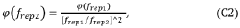
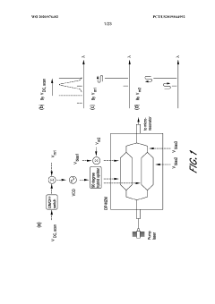
Compact microresonator frequency comb
PatentWO2020076402A1
Innovation
- The use of optimized microresonator actuators and modulators, including single-sideband modulators, graphene modulators, and microheaters, allows for precise control of carrier envelope offset frequency, repetition rate, and resonance offset frequency, enabling long-term locking and reduced noise, while minimizing cross-talk between parameters.
Optical devices comprising a micro-resonator frequency comb
PatentPendingUS20250246866A1
Innovation
- A micro-resonator frequency comb with a feedback control loop and control circuit stabilizes optical power and detuning by using a photo detector and control circuit to adjust the pump laser or resonator cavities, allowing for stable operation and tuning of the center frequency.
Fabrication Processes for Multi-Chip Photonic Systems
The fabrication of multi-chip photonic systems for microcomb coherence control represents a significant engineering challenge requiring precision manufacturing techniques across multiple domains. Current fabrication processes typically involve a combination of complementary metal-oxide-semiconductor (CMOS) compatible methods and specialized photonic integration approaches to achieve the necessary performance characteristics.
Silicon photonics platforms serve as the foundation for many multi-chip systems, utilizing 193nm deep ultraviolet lithography to define waveguide structures with sub-micron precision. These processes have evolved to accommodate feature sizes below 100nm, essential for controlling the dispersion properties critical to microcomb generation. The fabrication typically occurs in specialized foundries that have adapted semiconductor manufacturing techniques to the unique requirements of photonic circuits.
For microcomb resonator structures, high-Q factor materials processing is paramount. Silicon nitride (Si3N4) has emerged as a preferred material due to its low optical loss and favorable nonlinear properties. The deposition process typically involves low-pressure chemical vapor deposition (LPCVD) to create films with thicknesses ranging from 400nm to 1μm, followed by annealing steps to reduce hydrogen content and associated absorption losses.
Heterogeneous integration techniques have become increasingly important for combining different material platforms within multi-chip photonic systems. Techniques such as flip-chip bonding, die-to-wafer bonding, and wafer-to-wafer bonding enable the integration of III-V gain materials with silicon photonics, creating hybrid systems that leverage the advantages of each material platform. These processes require sub-micron alignment precision to ensure efficient optical coupling between chips.
Vertical coupling structures, including grating couplers and edge couplers, are critical components fabricated to facilitate chip-to-chip optical interconnections. These structures typically require specialized etching processes to create precisely angled surfaces or carefully controlled periodic structures that maximize coupling efficiency while minimizing back-reflections that could disrupt microcomb coherence.
Packaging processes represent the final critical fabrication step, involving hermetic sealing techniques and temperature stabilization systems. Advanced thermal management solutions, including integrated Peltier cooling elements and thermally conductive substrates, are implemented to maintain the precise temperature control required for stable microcomb operation across multiple chips.
Recent advances in fabrication have focused on improving yield and reproducibility through process standardization and automated testing protocols. These developments are essential for transitioning microcomb technology from laboratory demonstrations to commercially viable multi-chip photonic systems capable of reliable coherence control in real-world applications.
Standardization Efforts in Integrated Photonics
Standardization efforts in integrated photonics have become increasingly critical for the advancement of microcomb coherence control in multi-chip photonic systems. As the field evolves rapidly, industry stakeholders and research institutions are collaborating to establish common frameworks that enable interoperability, reliability, and scalability across different photonic platforms.
The IEEE P3186 working group has been actively developing standards specifically addressing coherent optical frequency comb generation and control in integrated photonic circuits. This initiative aims to standardize terminology, measurement techniques, and performance metrics for microcombs, facilitating consistent evaluation and comparison across different implementations and research groups.
The Photonic Integrated Circuit (PIC) Manufacturing Automation Standards Technical Advisory Group has recently expanded its scope to include specifications for multi-chip module interfaces, with particular emphasis on preserving coherence when signals traverse between chips. Their proposed standards include guidelines for chip-to-chip coupling efficiency, phase noise requirements, and thermal management considerations essential for maintaining coherence in distributed photonic systems.
On the international front, the International Electrotechnical Commission (IEC) has established the IEC 63296 series focusing on test methods for photonic integrated circuits. The upcoming extension, IEC 63296-3, will specifically address testing protocols for coherent light sources in multi-chip environments, providing manufacturers with standardized procedures to verify coherence preservation across chip boundaries.
The American National Standards Institute (ANSI) has partnered with the Optica Foundation (formerly OSA) to develop application-specific standards for quantum photonic systems that rely on microcomb coherence. These standards define minimum coherence time requirements and acceptable phase noise levels for applications ranging from optical computing to quantum key distribution.
Industry consortia such as the Integrated Photonics Systems Roadmap (IPSR) have established working groups dedicated to standardizing packaging techniques that minimize coherence degradation in multi-chip systems. Their recommendations include specifications for hermetic sealing, vibration isolation, and temperature stabilization to maintain phase relationships across physically separated photonic components.
The European Telecommunications Standards Institute (ETSI) has recently published technical specifications for coherent optical interconnects in data centers, incorporating requirements for microcomb-based frequency references and their integration in multi-chip architectures. These standards are particularly relevant for wavelength division multiplexing systems that leverage the precise frequency spacing of microcombs.
Unlock deeper insights with Patsnap Eureka Quick Research — get a full tech report to explore trends and direct your research. Try now!
Generate Your Research Report Instantly with AI Agent
Supercharge your innovation with Patsnap Eureka AI Agent Platform!