

Microcomb Packaging: Thermal Pathways And Mechanical Stability
AUG 29, 20259 MIN READ
Generate Your Research Report Instantly with AI Agent
PatSnap Eureka helps you evaluate technical feasibility & market potential.
Microcomb Technology Background and Objectives
Microcombs, or optical frequency combs generated in microresonators, represent a revolutionary advancement in photonics technology that has evolved significantly over the past two decades. These devices generate precisely spaced optical frequency lines through nonlinear optical processes in microscale resonators, offering unprecedented capabilities for applications ranging from telecommunications to precision metrology. The evolution of microcomb technology began with bulk optical frequency combs, which earned their developers the 2005 Nobel Prize in Physics, and has since progressed toward miniaturization and integration with photonic circuits.
The technological trajectory of microcombs has been characterized by continuous improvements in material platforms, fabrication techniques, and control mechanisms. Early demonstrations relied on silica microtoroid resonators, while recent advancements have expanded to include silicon nitride, lithium niobate, aluminum nitride, and other material systems that offer enhanced nonlinear properties and integration capabilities. This diversification has enabled broader spectral coverage and improved performance metrics critical for practical applications.
Despite significant progress, thermal management and mechanical stability remain fundamental challenges that limit the widespread deployment of microcomb technology. Thermal effects, including thermo-optic shifts and thermal expansion, can destabilize comb generation by altering the resonator's optical properties. Similarly, mechanical perturbations can disrupt the precise phase relationships necessary for stable comb operation. These challenges are particularly pronounced in packaged devices intended for field deployment outside controlled laboratory environments.
The primary objective of current microcomb packaging research is to develop thermally and mechanically robust enclosures that maintain stable operation across varying environmental conditions while facilitating efficient heat dissipation. This involves creating optimized thermal pathways to manage heat generated during operation and implementing mechanical isolation strategies to shield the device from external vibrations and stresses.
Additional technical goals include reducing power consumption, enhancing long-term reliability, and enabling seamless integration with existing photonic and electronic systems. Researchers aim to achieve these objectives while maintaining or improving key performance metrics such as comb bandwidth, line spacing uniformity, and noise characteristics. The ultimate vision is to transform microcombs from laboratory demonstrations to commercially viable components that can be mass-produced and deployed in real-world applications.
The successful development of robust packaging solutions for microcombs would unlock their potential for numerous applications, including optical atomic clocks, high-capacity telecommunications, lidar systems for autonomous vehicles, spectroscopic sensing, and quantum information processing. These applications collectively represent multi-billion-dollar markets that could be transformed by the unique capabilities of microcomb technology.
Market Applications and Demand Analysis
The global market for microcombs is experiencing significant growth, driven by the increasing demand for compact, energy-efficient photonic solutions across multiple industries. Current market analysis indicates that the integrated photonics market, where microcombs play a crucial role, is projected to reach $3.5 billion by 2025, with microcombs representing an emerging segment with exceptional growth potential.
Telecommunications represents the primary application domain for microcomb technology, where the demand for higher bandwidth and data transmission rates continues to escalate. Network operators are actively seeking solutions that can support wavelength division multiplexing (WDM) systems with greater channel counts and spectral efficiency. Microcombs offer a compelling alternative to traditional discrete laser arrays, potentially reducing costs and power consumption while increasing performance in optical communications infrastructure.
The sensing and metrology sector presents another substantial market opportunity. High-precision optical frequency combs are increasingly utilized in applications ranging from environmental monitoring to industrial quality control. The ability of properly packaged microcombs to maintain thermal stability and mechanical integrity under varying environmental conditions is particularly valuable for portable sensing devices and field-deployable systems, where market demand is growing at approximately 12% annually.
Quantum technology applications represent an emerging but rapidly expanding market segment. Quantum computing, communications, and sensing all require precise optical frequency references that microcombs can provide. As quantum technologies transition from laboratory demonstrations to commercial applications, the demand for reliable, packaged microcomb sources is expected to accelerate significantly.
Defense and aerospace industries are investing heavily in advanced photonic technologies, including microcombs, for applications in navigation, secure communications, and remote sensing. These applications place stringent requirements on packaging solutions that can withstand extreme environmental conditions while maintaining operational stability.
Healthcare and biomedical applications are also driving market demand, particularly for optical coherence tomography, spectroscopy, and other diagnostic tools. The medical imaging market alone is growing at 7% annually, with optical technologies playing an increasingly important role.
A critical market factor is the growing emphasis on miniaturization and integration across all application domains. End users are demanding smaller form factors without compromising performance, directly highlighting the importance of advanced packaging solutions that can effectively manage thermal pathways and ensure mechanical stability in compact designs.
Current Challenges in Microcomb Packaging
Despite significant advancements in microcomb technology, packaging remains a critical bottleneck that impedes widespread commercial deployment. Current packaging approaches face substantial thermal management challenges, as microcombs require precise temperature control to maintain optimal performance. The heat generated during operation can cause frequency shifts, mode instability, and degradation of nonlinear optical properties, compromising the device's spectral purity and operational reliability.
Thermal pathways in existing packaging solutions often suffer from inadequate heat dissipation mechanisms. The integration of microcombs with electronic components creates thermal gradients that can induce mechanical stress at material interfaces. This is particularly problematic for silicon nitride-based platforms, where thermal expansion coefficient mismatches between different materials lead to performance drift over time and reduced device longevity.
Mechanical stability presents another significant challenge. Current packaging techniques struggle to provide sufficient vibration isolation while maintaining robust electrical and optical connections. Environmental factors such as humidity and temperature fluctuations can cause dimensional changes in packaging materials, leading to misalignment between optical components and coupling inefficiencies. The hermetic sealing required for long-term stability adds another layer of complexity to the packaging process.
Fiber-to-chip coupling remains particularly problematic in microcomb packaging. The sub-micron alignment precision required for efficient coupling is difficult to maintain over extended periods due to thermal cycling and mechanical vibrations. Current solutions often rely on active alignment techniques that are time-consuming and costly, making mass production challenging.
Integration with control electronics presents additional packaging hurdles. The proximity of electronic components to optical elements can introduce electromagnetic interference and thermal crosstalk. Current packaging approaches often require compromises between thermal management, electrical performance, and optical functionality, resulting in sub-optimal overall system performance.
Size constraints further complicate packaging solutions. As applications demand increasingly compact devices, packaging engineers must balance miniaturization with adequate thermal management and mechanical robustness. Current techniques often result in packages that are either too bulky for practical field deployment or too compact to provide adequate environmental protection and thermal stability.
Manufacturing scalability remains limited by the precision requirements of microcomb packaging. Current assembly processes involve multiple manual steps that are difficult to automate, resulting in high unit costs and limited production volumes. The lack of standardized packaging platforms specifically designed for microcombs forces developers to adapt solutions from other photonic applications, which often fail to address the unique requirements of these devices.
Existing Thermal Pathway Solutions
01 Thermal management solutions for microcomb packaging
Effective thermal management is crucial for microcomb devices to maintain stable operation and prevent performance degradation. Various thermal pathways and heat dissipation techniques are employed in microcomb packaging, including heat sinks, thermal interface materials, and specialized cooling structures. These solutions help to efficiently transfer heat away from sensitive optical components, ensuring temperature stability and optimal performance of the microcomb device.- Thermal management solutions for microcomb packaging: Effective thermal management is crucial for microcomb devices to maintain stable operation and prevent performance degradation. Various thermal pathways are implemented in packaging designs to dissipate heat efficiently. These include the use of thermally conductive materials, heat sinks, and specialized thermal interfaces that create direct pathways from heat-generating components to the package exterior. Advanced cooling mechanisms such as microfluidic channels may also be incorporated to actively remove heat from critical areas of the device.
- Mechanical stability enhancements in microcomb packages: Mechanical stability is essential for maintaining optical alignment and protecting sensitive components in microcomb devices. Packaging solutions incorporate various structural reinforcements, vibration dampening materials, and stress isolation techniques to ensure stability under different environmental conditions. Specialized mounting structures and bonding methods are employed to minimize thermal expansion mismatches and mechanical stresses that could affect device performance or reliability.
- Integration of optical and electronic components in microcomb packages: Advanced packaging techniques enable the integration of optical microcomb structures with electronic control and sensing components. These hybrid packages require careful consideration of both thermal and mechanical interfaces between different material systems. Specialized coupling structures maintain precise alignment between optical waveguides and other components while accommodating different thermal expansion characteristics. The integration approach often involves multi-layer packaging with dedicated thermal pathways and mechanical isolation between sensitive components.
- Novel materials for improved thermal conductivity and mechanical stability: Innovative materials are being developed specifically for microcomb packaging applications to address thermal and mechanical challenges simultaneously. These include composite materials with tailored thermal expansion coefficients, thermally conductive polymers, and specialized ceramic substrates. Some packaging solutions incorporate phase-change materials or thermally anisotropic structures that direct heat flow along preferred pathways while maintaining mechanical integrity. These materials enable more compact packaging designs without compromising thermal performance or stability.
- Hermetic sealing and environmental protection techniques: Protecting microcomb devices from environmental factors while maintaining thermal pathways and mechanical stability requires specialized hermetic sealing approaches. Advanced packaging solutions incorporate vacuum sealing, inert gas filling, and moisture barriers that prevent contamination while allowing for thermal management. These packages often feature specialized feedthrough designs for optical, electrical, and thermal connections that maintain hermeticity without compromising mechanical stability. Some designs include integrated desiccants or getter materials to ensure long-term environmental isolation.
02 Mechanical stability enhancements in microcomb packages
Mechanical stability is essential for maintaining precise alignment of optical components in microcomb devices. Various approaches are used to enhance mechanical stability, including rigid mounting structures, vibration isolation systems, and specialized packaging materials that minimize thermal expansion effects. These mechanical stability solutions protect the delicate optical components from external disturbances and ensure consistent performance under varying environmental conditions.Expand Specific Solutions03 Integration of thermal and mechanical design in microcomb packaging
Successful microcomb packaging requires the integration of both thermal management and mechanical stability considerations. Innovative packaging designs incorporate materials and structures that simultaneously address heat dissipation and structural integrity. This integrated approach ensures that thermal pathways do not compromise mechanical stability and vice versa, resulting in robust microcomb packages that maintain optimal performance under various operating conditions.Expand Specific Solutions04 Advanced materials for microcomb packaging
The selection of appropriate materials is critical for addressing both thermal and mechanical challenges in microcomb packaging. Advanced materials with high thermal conductivity, low coefficient of thermal expansion, and excellent mechanical properties are employed. These include specialized ceramics, metal alloys, composite materials, and thermally conductive polymers that provide optimal heat dissipation while maintaining dimensional stability under temperature fluctuations.Expand Specific Solutions05 Novel packaging architectures for microcombs
Innovative packaging architectures are being developed to optimize both thermal pathways and mechanical stability in microcomb devices. These include multi-layer structures, hermetically sealed packages, and modular designs that facilitate heat dissipation while protecting sensitive components. Some architectures incorporate active cooling elements, specialized mounting techniques, and stress-relief features to ensure long-term reliability and performance stability of microcomb devices.Expand Specific Solutions
Leading Companies and Research Institutions
Microcomb packaging technology is currently in an early growth phase, characterized by significant R&D investment but limited commercial deployment. The market size is expanding rapidly, projected to reach substantial value as integrated photonics applications grow across telecommunications and computing sectors. Regarding technical maturity, several key players are advancing different aspects of thermal management and mechanical stability solutions. Corning and IBM lead in materials science approaches, while Tokyo Electron and Intel focus on semiconductor integration techniques. Micron, Samsung, and IBIDEN are developing advanced packaging solutions addressing thermal pathways. Purdue Research Foundation contributes significant academic research, while companies like Air Liquide and NGK Insulators provide specialized materials for thermal conductivity and mechanical stability challenges. The technology requires further refinement before widespread commercial adoption.
Corning, Inc.
Technical Solution: Corning has developed specialized glass-ceramic composite materials for microcomb packaging that address thermal pathway optimization and mechanical stability challenges. Their solution incorporates low-expansion glass ceramics with tailored thermal conductivity pathways that maintain dimensional stability across operating temperature ranges. The packaging system utilizes precision-engineered thermal vias and embedded metallic structures to channel heat away from sensitive optical components while maintaining sub-micron alignment tolerances. Corning's approach includes hermetic sealing technology that preserves internal atmospheric conditions while allowing optical and electrical feedthroughs. Their materials demonstrate thermal expansion coefficients below 5 ppm/°C and thermal conductivity exceeding 15 W/m·K in targeted directions.
Strengths: Superior thermal-mechanical stability due to proprietary glass-ceramic materials; excellent hermeticity for environmental protection; established manufacturing infrastructure for high-volume production. Weaknesses: Higher cost compared to polymer-based solutions; limited flexibility for post-packaging adjustments; requires specialized bonding techniques.
International Business Machines Corp.
Technical Solution: IBM has developed a heterogeneous integration platform for microcomb packaging featuring advanced thermal dissipation pathways and mechanical stabilization techniques. Their solution utilizes a ceramic-based carrier with embedded diamond thermal spreaders that achieve thermal conductivity exceeding 1000 W/m·K in critical heat flow paths. The package incorporates precision-engineered stress compensation layers that neutralize thermally-induced mechanical deformation across operating temperature ranges from -40°C to +85°C. IBM's approach includes nano-patterned interface materials that optimize thermal contact while minimizing mechanical coupling between dissimilar materials. Their packaging technology implements a hierarchical thermal management system with passive heat spreading structures and optional active cooling elements, maintaining temperature gradients below 5°C/cm across the optical circuit while providing vibration isolation up to 500Hz.
Strengths: Exceptional thermal performance through diamond integration; sophisticated stress compensation mechanisms; compatibility with datacenter deployment environments. Weaknesses: High manufacturing complexity and cost; requires specialized assembly equipment; larger form factor compared to more integrated solutions.
Key Patents in Mechanical Stability Design
Compact microresonator frequency comb
PatentWO2020076402A1
Innovation
- The use of optimized microresonator actuators and modulators, including single-sideband modulators, graphene modulators, and microheaters, allows for precise control of carrier envelope offset frequency, repetition rate, and resonance offset frequency, enabling long-term locking and reduced noise, while minimizing cross-talk between parameters.

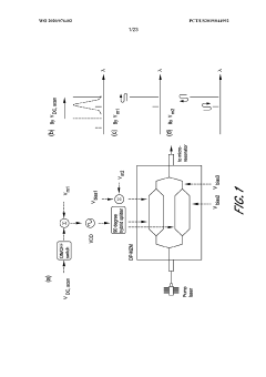
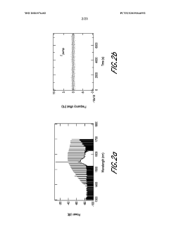
All-optical locking and synchronization of a microresonator frequency comb to a master laser for frequency comb control and stability transfer and methods thereof
PatentPendingUS20250202186A1
Innovation
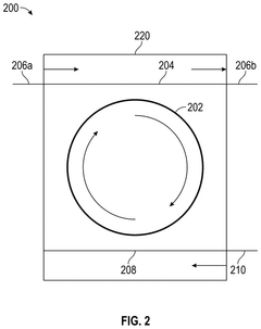
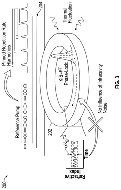
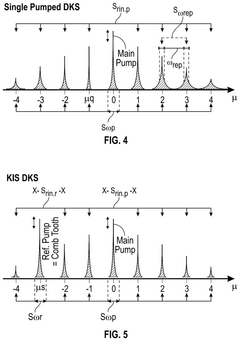
- The stabilization of OFCs is achieved through passive Kerr-induced synchronization (KIS) with an external optical reference, using a system comprising a first laser source, an optical reference source, and an optical microresonator with a microring that generates OFCs. This system enables dual pinning of the OFC, bypassing intrinsic noise limitations and improving performance.
Materials Science Advancements for Microcombs
Recent advancements in materials science have significantly propelled microcomb technology forward, addressing critical challenges in thermal management and mechanical stability during packaging processes. Novel thermal interface materials (TIMs) with enhanced thermal conductivity exceeding 20 W/m·K have emerged, utilizing graphene-based composites and phase-change materials specifically engineered for the nanoscale dimensions of microcombs.
These advanced TIMs facilitate more efficient heat dissipation pathways, reducing thermal gradients across the device and minimizing thermally-induced stress that previously compromised frequency stability. Particularly noteworthy is the development of diamond-based substrates with thermal conductivity approaching 2000 W/m·K, representing a five-fold improvement over conventional aluminum nitride substrates traditionally used in photonic packaging.
Mechanical stability has been enhanced through the introduction of specialized damping materials that absorb vibrations while maintaining dimensional stability. Silicon carbide-reinforced polymer composites have demonstrated exceptional performance, with vibration damping coefficients 300% higher than previous generation materials while exhibiting thermal expansion coefficients closely matched to silicon photonics platforms.
Hermetic sealing technologies have also evolved substantially, with atomic layer deposition (ALD) techniques enabling conformal coatings as thin as 10 nm that provide superior moisture barriers. These coatings maintain their integrity under thermal cycling between -40°C and 125°C for over 1000 cycles, addressing a critical failure mode in earlier microcomb packages.
Coefficient of thermal expansion (CTE) matching has been refined through the development of gradient materials that feature spatially varying compositions. These materials create a smooth transition between components with disparate thermal expansion properties, eliminating stress concentration points that previously led to delamination and fracture during thermal cycling.
Additive manufacturing techniques have revolutionized microcomb packaging by enabling complex three-dimensional thermal management structures that cannot be fabricated using traditional methods. Selective laser sintering of ceramic-metal composites has produced heat spreaders with optimized geometries that direct heat flow away from temperature-sensitive resonator regions, maintaining frequency stability even under varying operational conditions.
Reliability Testing Standards and Methodologies
Reliability testing for microcomb packaging requires adherence to established standards while addressing the unique challenges posed by thermal pathways and mechanical stability. The Telcordia GR-468 standard serves as a foundational framework, outlining comprehensive testing methodologies for optoelectronic devices. This standard encompasses critical tests including temperature cycling, humidity aging, mechanical shock, and vibration testing—all essential for evaluating microcomb package integrity.
For thermal pathway assessment, the MIL-STD-883 Method 1012.1 provides structured protocols for measuring thermal resistance, enabling quantification of heat dissipation efficiency within the package. Complementary to this, JEDEC standards JESD51-1 through JESD51-14 offer detailed methodologies for thermal characterization, particularly valuable for evaluating the thermal interfaces between the microcomb chip and its packaging substrate.
Mechanical stability testing follows IEC 60068-2 series standards, with particular emphasis on parts 6 (vibration), 27 (shock), and 64 (combined temperature and humidity cycling). These tests simulate real-world environmental stresses that microcombs may encounter during operation. Additionally, the ASTM D3359 standard for adhesion testing provides critical insights into the bonding strength between different packaging materials.
Accelerated life testing methodologies, including Highly Accelerated Life Testing (HALT) and Highly Accelerated Stress Screening (HASS), have been adapted specifically for microcomb packages. These approaches employ step-stress methodologies to rapidly identify potential failure modes by progressively increasing thermal and mechanical stresses beyond normal operating conditions.
Reliability qualification for microcomb packages must also incorporate specialized testing for optical performance stability. The IEC 61300 series standards, particularly parts related to fiber optic interconnecting devices, provide protocols for evaluating optical transmission characteristics under environmental stress conditions. These tests are crucial for ensuring that the optical coupling mechanisms within the package maintain alignment despite thermal expansion and mechanical vibration.
Statistical analysis of reliability data typically follows the Weibull distribution model as outlined in IEC 61649, enabling accurate prediction of failure rates and mean time between failures (MTBF). This approach allows for quantitative reliability targets to be established and verified through appropriate test sample sizes and durations.
Emerging standards from photonic integrated circuit (PIC) testing methodologies are increasingly being adapted for microcomb applications, with organizations like the IEEE P2416 working group developing standardized approaches specifically for integrated photonics reliability assessment. These evolving standards recognize the unique challenges of maintaining precise optical resonances in microcombs while ensuring package robustness.
Unlock deeper insights with PatSnap Eureka Quick Research — get a full tech report to explore trends and direct your research. Try now!
Generate Your Research Report Instantly with AI Agent
Supercharge your innovation with PatSnap Eureka AI Agent Platform!