

Chip-Scale Comb Sources For Microwave Synthesis Applications
AUG 29, 20259 MIN READ
Generate Your Research Report Instantly with AI Agent
PatSnap Eureka helps you evaluate technical feasibility & market potential.
Chip-Scale Comb Technology Background and Objectives
Optical frequency combs have emerged as a revolutionary technology in precision metrology, enabling unprecedented accuracy in frequency measurements. The evolution of this technology has progressed from bulky laboratory setups to chip-scale implementations, marking a significant advancement in miniaturization and integration capabilities. Chip-scale comb sources represent the convergence of photonics, microelectronics, and precision engineering, offering compact solutions for applications requiring precise frequency control.
The historical trajectory of frequency comb technology began with the groundbreaking work of Theodor Hänsch and John Hall, who were awarded the Nobel Prize in Physics in 2005 for their contributions to laser-based precision spectroscopy. Traditional frequency combs relied on mode-locked lasers and complex optical setups, limiting their practical deployment outside specialized laboratories. The transition to chip-scale implementations began in the early 2010s, driven by advances in integrated photonics and microfabrication techniques.
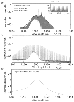
Microresonator-based frequency combs, particularly those utilizing Kerr nonlinear optical processes, have emerged as a promising approach for chip-scale integration. These devices leverage high-quality factor optical resonators to enhance nonlinear interactions, enabling comb generation with reduced power requirements and footprint. Parallel developments in materials science, particularly in silicon nitride, silicon, and III-V semiconductors, have further accelerated the miniaturization process.
The primary objective of chip-scale comb technology for microwave synthesis applications is to develop compact, energy-efficient, and cost-effective frequency comb sources capable of generating stable and low-noise microwave signals. These sources aim to replace traditional electronic oscillators in various applications, including telecommunications, radar systems, and scientific instrumentation, offering superior phase noise performance and frequency stability.
Additional technical goals include achieving wider comb spacing for direct microwave generation, enhancing power efficiency to enable battery-powered operation, improving thermal stability for field deployment, and developing robust packaging solutions for environmental protection. Integration with electronic components through CMOS-compatible processes represents another critical objective, facilitating seamless incorporation into existing technological ecosystems.
The long-term vision encompasses the development of fully integrated photonic-electronic systems where chip-scale frequency combs serve as the core timing and frequency reference. This integration would enable new capabilities in portable atomic clocks, high-precision navigation systems, terahertz spectroscopy, and quantum information processing. As the technology matures, we anticipate a transition from specialized applications to widespread commercial adoption, potentially revolutionizing fields ranging from telecommunications to healthcare diagnostics.
The historical trajectory of frequency comb technology began with the groundbreaking work of Theodor Hänsch and John Hall, who were awarded the Nobel Prize in Physics in 2005 for their contributions to laser-based precision spectroscopy. Traditional frequency combs relied on mode-locked lasers and complex optical setups, limiting their practical deployment outside specialized laboratories. The transition to chip-scale implementations began in the early 2010s, driven by advances in integrated photonics and microfabrication techniques.
Microresonator-based frequency combs, particularly those utilizing Kerr nonlinear optical processes, have emerged as a promising approach for chip-scale integration. These devices leverage high-quality factor optical resonators to enhance nonlinear interactions, enabling comb generation with reduced power requirements and footprint. Parallel developments in materials science, particularly in silicon nitride, silicon, and III-V semiconductors, have further accelerated the miniaturization process.
The primary objective of chip-scale comb technology for microwave synthesis applications is to develop compact, energy-efficient, and cost-effective frequency comb sources capable of generating stable and low-noise microwave signals. These sources aim to replace traditional electronic oscillators in various applications, including telecommunications, radar systems, and scientific instrumentation, offering superior phase noise performance and frequency stability.
Additional technical goals include achieving wider comb spacing for direct microwave generation, enhancing power efficiency to enable battery-powered operation, improving thermal stability for field deployment, and developing robust packaging solutions for environmental protection. Integration with electronic components through CMOS-compatible processes represents another critical objective, facilitating seamless incorporation into existing technological ecosystems.
The long-term vision encompasses the development of fully integrated photonic-electronic systems where chip-scale frequency combs serve as the core timing and frequency reference. This integration would enable new capabilities in portable atomic clocks, high-precision navigation systems, terahertz spectroscopy, and quantum information processing. As the technology matures, we anticipate a transition from specialized applications to widespread commercial adoption, potentially revolutionizing fields ranging from telecommunications to healthcare diagnostics.
Market Analysis for Microwave Synthesis Applications
The global market for microwave synthesis applications utilizing chip-scale comb sources is experiencing robust growth, driven by increasing demands for high-precision frequency generation in telecommunications, radar systems, and scientific instrumentation. Current market valuations indicate that the microwave synthesis sector reached approximately 3.2 billion USD in 2022, with projections suggesting a compound annual growth rate of 7.8% through 2028.
The telecommunications segment represents the largest market share, accounting for nearly 42% of total demand. This dominance stems from the critical need for precise frequency references in 5G infrastructure deployment and the ongoing development of 6G technologies. Network operators and equipment manufacturers are increasingly seeking compact, energy-efficient solutions that can deliver superior phase noise performance while reducing overall system complexity.
Defense and aerospace applications constitute the second-largest market segment at 28%, where chip-scale comb sources are revolutionizing radar systems, electronic warfare capabilities, and satellite communications. The inherent advantages of integrated photonic solutions—including reduced size, weight, and power consumption—make them particularly attractive for deployment in space-constrained environments such as unmanned aerial vehicles and compact satellite platforms.
Scientific and metrology applications represent a smaller but rapidly growing segment at 17% of the market. Research institutions and national laboratories are adopting chip-scale frequency comb technology for applications ranging from high-precision spectroscopy to quantum information processing. This segment is expected to grow at the fastest rate over the next five years as the technology matures and becomes more accessible to a broader range of scientific disciplines.
Regional analysis reveals North America leading with 38% market share, followed by Europe (29%) and Asia-Pacific (24%). However, the Asia-Pacific region is projected to exhibit the highest growth rate, driven by substantial investments in telecommunications infrastructure and defense modernization programs in countries like China, South Korea, and Japan.
Customer requirements are evolving toward solutions offering greater integration density, lower power consumption, and enhanced environmental stability. Market surveys indicate that 76% of potential customers prioritize reliability and performance consistency across varying operational conditions, while 64% emphasize the importance of seamless integration with existing systems.
The competitive landscape features both established photonics companies and emerging startups, with increasing collaboration between chip manufacturers, system integrators, and end-users. This ecosystem approach is accelerating commercialization timelines and expanding addressable markets through customized solutions tailored to specific application requirements.
Technical Challenges in Chip-Scale Frequency Comb Development
Despite significant advancements in chip-scale frequency comb technology, several critical technical challenges continue to impede widespread implementation in microwave synthesis applications. The primary obstacle remains achieving reliable and efficient nonlinear optical processes within the confined dimensions of integrated photonic platforms. The generation of stable frequency combs requires precise control of dispersion characteristics, which becomes increasingly difficult at the microscale where material properties and fabrication tolerances significantly impact performance.
Power efficiency presents another substantial hurdle. Current chip-scale comb sources typically require pump powers in the range of tens to hundreds of milliwatts to initiate and sustain the comb generation process. This power requirement limits their integration into portable or power-constrained systems, particularly for applications requiring battery operation or deployment in remote locations.
Thermal management constitutes a critical challenge that directly affects frequency stability. The high optical power densities within waveguides generate significant heat, creating thermal gradients that alter the refractive index and resonance conditions. These thermal effects can destabilize the comb, causing frequency drift and phase noise degradation that severely impact microwave synthesis performance.
The spectral coverage of chip-scale combs remains limited compared to their bulk counterparts. While applications in microwave synthesis primarily require combs spanning tens to hundreds of gigahertz, achieving broader bandwidths with uniform power distribution across comb lines continues to challenge researchers. This limitation restricts the frequency range and flexibility of synthesized microwave signals.
Phase noise performance represents perhaps the most significant barrier to adoption in precision microwave applications. Current chip-scale combs exhibit phase noise levels that, while improving, still fall short of requirements for advanced radar, communication systems, and metrology applications. The intrinsic noise of the pump laser, thermorefractive noise, and various technical noise sources contribute to this limitation.
Integration with electronic components presents additional challenges. Efficient interfaces between photonic and electronic domains require careful design to minimize conversion losses and maintain signal integrity. Furthermore, packaging solutions must address thermal management, mechanical stability, and protection from environmental factors while maintaining optical coupling efficiency.
Fabrication reproducibility remains problematic, with device-to-device variations affecting comb initiation thresholds, spectral characteristics, and overall performance. These variations stem from nanoscale imperfections in lithography, etching processes, and material deposition, highlighting the need for more robust designs and improved manufacturing techniques to enable commercial-scale production.
Current Chip-Scale Comb Architectures for Microwave Generation
01 Integrated photonic chip-scale comb sources
Integrated photonic platforms enable the miniaturization of optical frequency comb sources to chip scale. These designs incorporate microresonators, waveguides, and other photonic components directly on semiconductor substrates to generate broadband optical frequency combs. The integration allows for compact, stable, and power-efficient comb generation suitable for various applications including telecommunications, spectroscopy, and sensing.- Integrated Photonic Frequency Comb Sources: Chip-scale photonic frequency comb sources integrate optical frequency comb generation capabilities onto semiconductor chips. These devices typically use microresonators or other photonic structures to generate multiple, equally spaced frequency lines from a single laser source. The integration enables compact, power-efficient comb sources suitable for applications in telecommunications, spectroscopy, and precision metrology.
- Semiconductor Packaging for Optical Comb Sources: Advanced packaging technologies for chip-scale comb sources focus on integrating optical components with electronic control circuitry. These packaging solutions address thermal management, optical coupling efficiency, and mechanical stability challenges. Techniques include flip-chip bonding, through-silicon vias, and specialized substrate materials to enable reliable operation of miniaturized comb sources in various environmental conditions.
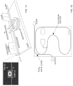
- Microresonator-Based Comb Generation: Microresonator structures are fundamental to chip-scale comb sources, utilizing high-Q optical cavities to enhance nonlinear optical effects. These structures can be fabricated using various materials including silicon nitride, silicon dioxide, or III-V semiconductors. The design parameters of the microresonator, such as free spectral range, quality factor, and dispersion characteristics, determine the properties of the generated frequency comb.
- Integration with Silicon Photonics: Silicon photonics platforms enable the integration of comb sources with other optical components such as modulators, filters, and photodetectors on a single chip. This integration approach leverages CMOS-compatible fabrication processes to create complex photonic integrated circuits that incorporate frequency comb generation. The silicon photonics approach offers advantages in terms of scalability, cost-effectiveness, and compatibility with electronic integrated circuits.
- Novel Materials and Structures for Enhanced Comb Performance: Advanced materials and novel structural designs are being developed to improve the performance of chip-scale comb sources. These innovations include heterogeneous integration of III-V materials with silicon, use of 2D materials like graphene, and engineered nonlinear optical materials. Such approaches aim to enhance key performance metrics including spectral bandwidth, power efficiency, phase noise, and stability of the generated frequency combs.
02 Semiconductor packaging for comb source devices
Advanced packaging technologies are essential for chip-scale comb sources to ensure proper thermal management, electrical connectivity, and optical coupling. These packaging solutions include flip-chip bonding, through-silicon vias, and specialized optical interfaces that maintain the performance of the comb source while providing protection from environmental factors. The packaging architecture also facilitates integration with other electronic and photonic components in compact systems.Expand Specific Solutions03 Nonlinear optical materials for comb generation
Specialized nonlinear optical materials are incorporated into chip-scale platforms to enhance frequency comb generation. These materials exhibit strong third-order nonlinearities necessary for four-wave mixing and other nonlinear processes that create and stabilize frequency combs. The selection and engineering of these materials, including silicon nitride, aluminum nitride, and lithium niobate thin films, are crucial for achieving desired comb characteristics such as bandwidth, stability, and power efficiency.Expand Specific Solutions04 Microelectronic fabrication techniques for comb sources
Advanced microelectronic fabrication methods are employed to create the precise structures needed for chip-scale comb sources. These techniques include high-precision lithography, etching processes, and material deposition methods that enable the creation of nanoscale features with the required dimensional accuracy. The fabrication processes are optimized to produce low-loss waveguides, high-Q resonators, and other critical components while ensuring compatibility with standard semiconductor manufacturing flows.Expand Specific Solutions05 Pump laser integration and control systems
Efficient pump laser integration and precise control systems are essential components of chip-scale comb sources. These systems include on-chip or hybrid-integrated pump lasers, thermal control elements, and electronic feedback circuits that maintain the stability of the comb generation process. Advanced control algorithms and sensing mechanisms are implemented to adjust operating parameters in real-time, ensuring consistent comb performance despite environmental variations or aging effects.Expand Specific Solutions
Leading Companies and Research Institutions in Photonic Integration
Chip-scale comb sources for microwave synthesis applications are currently in an early growth phase, with the market expanding as technology matures. The competitive landscape features academic institutions (Columbia University, Caltech, EPFL) driving fundamental research alongside established industrial players (IMRA America, Raytheon, Applied Materials) commercializing solutions. Huawei and ETRI are investing heavily in integrated photonics platforms, while specialized companies like Toptica Photonics focus on precision laser systems. Government research entities (CSIR, US Government) provide funding support. The technology is transitioning from laboratory demonstrations to commercial viability, with key challenges in integration density, power consumption, and phase noise performance still being addressed by leading players.
IMRA America, Inc.
Technical Solution: IMRA America has developed proprietary chip-scale frequency comb technology based on their expertise in ultrafast fiber lasers and integrated photonics. Their approach utilizes lithium niobate on insulator (LNOI) platform to create highly efficient electro-optic frequency comb generators. The technology features periodically poled lithium niobate (PPLN) waveguides with engineered dispersion profiles that enable broadband comb generation with flat spectral envelopes. For microwave synthesis applications, IMRA's solution incorporates on-chip optical filters and high-speed photodetectors to extract ultra-stable microwave signals directly from the optical domain. Their implementation achieves frequency combs spanning over 100 nm with line spacing precisely controlled by RF drive signals (typically 10-40 GHz). Recent innovations include hybrid integration with semiconductor optical amplifiers to boost optical power and improve signal-to-noise ratio in the generated microwave signals, achieving phase noise performance below -140 dBc/Hz at 10 kHz offset for a 10 GHz carrier.
Strengths: Exceptional electro-optic efficiency enabling low-power operation; precise control over comb line spacing; mature manufacturing process leveraging telecom industry infrastructure. Weaknesses: Temperature sensitivity of lithium niobate requiring active stabilization; limited optical power handling compared to some competing platforms; higher propagation losses than silicon nitride waveguides.
California Institute of Technology
Technical Solution: Caltech has pioneered chip-scale optical frequency comb technology based on high-Q silicon nitride microresonators. Their approach utilizes the Kerr nonlinear effect in these resonators to generate broadband frequency combs from a single continuous-wave laser source. The technology features integrated photonic circuits that combine microresonators with on-chip waveguides, photodetectors, and control electronics. Caltech's implementation achieves octave-spanning frequency combs with line spacing in the microwave range (typically 10-100 GHz), enabling direct microwave synthesis through optical-to-electrical conversion. Their recent advancements include soliton microcomb generation with enhanced stability and phase noise characteristics suitable for precision timing applications. The integrated nature of their solution allows for significant miniaturization compared to traditional microwave sources, with devices measuring only a few square millimeters while maintaining performance comparable to benchtop systems.
Strengths: Exceptional frequency stability and low phase noise performance; high level of integration enabling true chip-scale implementation; mature fabrication process compatible with CMOS manufacturing. Weaknesses: Requires precise temperature control for stable operation; power consumption challenges for portable applications; limited output power compared to conventional microwave oscillators.
Key Patents and Breakthroughs in Integrated Photonic Combs
Signal processing apparatus and method for transmitting and receiving coherent parallel optical signals
PatentActiveUS20180083599A1
Innovation
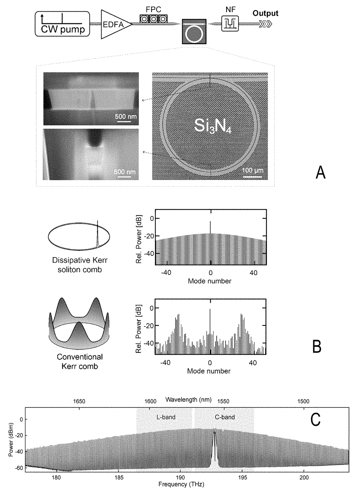
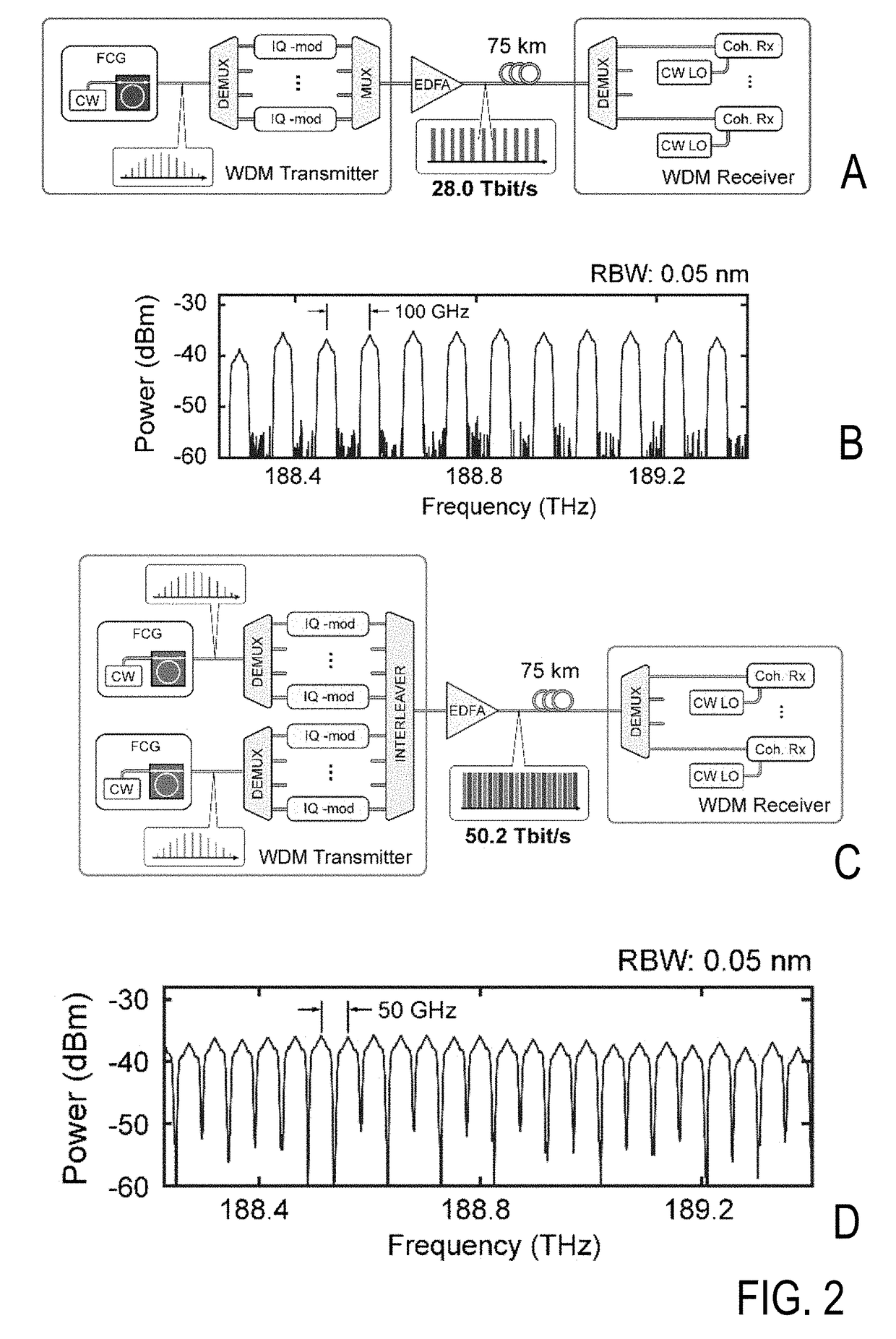
- The use of dissipative Kerr soliton (DKS) micro-resonator-based frequency combs, which generate smooth and broadband spectral envelopes, enabling the creation of multiple equidistant optical carriers and reference signals, thereby increasing data rates and simplifying receiver complexity through interleaved Kerr combs at both transmitter and receiver sides.
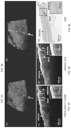
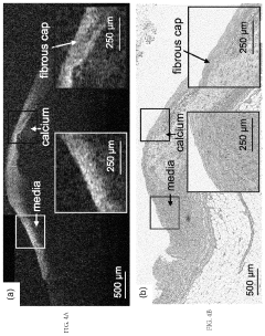
Microresonator-frequency-comb-based platform for clinical high-resolution optical coherence tomography
PatentActiveUS11859972B2
Innovation
- A microresonator-frequency-comb-based platform using high-Q silicon nitride resonators and distributed feedback lasers generates broadband frequency combs, overcoming the bandwidth-power trade-off and enabling sub-micrometer axial resolution and deeper tissue penetration, compatible with standard OCT systems.
Integration Strategies for Photonic-Electronic Systems
The integration of photonic and electronic systems represents a critical challenge in realizing practical chip-scale comb sources for microwave synthesis applications. Current integration strategies focus on three primary approaches: monolithic integration, hybrid integration, and heterogeneous integration, each offering distinct advantages and limitations for different application scenarios.
Monolithic integration, where both photonic and electronic components are fabricated on the same substrate, offers the highest level of miniaturization and reliability. Silicon photonics platforms have emerged as the leading approach, allowing for the co-integration of optical frequency combs with electronic control circuitry. Recent advances in CMOS-compatible processes have enabled the fabrication of nonlinear optical resonators alongside electronic components, significantly reducing parasitic effects and improving overall system performance.
Hybrid integration techniques involve the assembly of separately fabricated photonic and electronic chips, typically using flip-chip bonding or wire bonding technologies. This approach allows for the optimization of each subsystem independently, utilizing the most appropriate material platform for each function. For microwave synthesis applications, hybrid integration permits the combination of high-Q optical resonators made from materials like silicon nitride or lithium niobate with specialized electronic circuits for comb stabilization and control.
Heterogeneous integration represents a middle ground, where different material systems are combined during the fabrication process. Techniques such as wafer bonding and epitaxial growth enable the integration of III-V gain materials with silicon photonics, addressing the challenge of incorporating active optical components. This approach has shown particular promise for self-referenced frequency combs that require both passive nonlinear elements and active components.
Packaging considerations play a crucial role in system integration, particularly for applications requiring thermal stability and low phase noise. Advanced thermal management solutions, including microchannel cooling and thermoelectric controllers, have been developed to maintain precise operating conditions for nonlinear optical resonators. Additionally, RF signal integrity must be preserved through careful design of electrical interconnects and shielding.
Interface optimization between photonic and electronic domains represents another key challenge. High-speed photodetectors with bandwidths exceeding 100 GHz are being developed to efficiently convert optical signals to the electrical domain, while specialized electronic circuits for phase-locked loops and servo control systems enable precise comb stabilization. Novel co-design methodologies that simultaneously consider both optical and electronic performance metrics are emerging as essential tools for system optimization.
Performance Metrics and Standardization Requirements
To establish a robust framework for evaluating chip-scale comb sources in microwave synthesis applications, standardized performance metrics are essential. Phase noise represents a critical parameter, with industry standards typically requiring levels below -120 dBc/Hz at 10 kHz offset for high-precision applications. Frequency stability metrics must address both short-term stability (Allan deviation <10^-12 at 1-second integration) and long-term drift (typically <1 ppm/year). These specifications ensure reliable operation in demanding environments such as radar systems and telecommunications infrastructure.
Spectral purity metrics require quantification of spurious emissions, with standards typically mandating levels below -70 dBc across the operational bandwidth. Power efficiency standards are increasingly important, with current benchmarks targeting conversion efficiencies exceeding 20% for integrated solutions. Size constraints for chip-scale implementations generally specify maximum dimensions of 10×10 mm² with heights under 2 mm to facilitate integration into compact systems.
Temperature stability represents another crucial metric, with performance variations typically required to remain within ±0.5 ppm across operational temperature ranges (-40°C to +85°C for commercial applications, -55°C to +125°C for military-grade systems). Tuning range specifications generally demand at least 10% of the center frequency with sub-microsecond settling times for agile applications.
Standardization efforts are being led by several organizations including the IEEE Microwave Theory and Techniques Society (MTT-S), which has established working groups specifically addressing integrated photonic microwave sources. The International Telecommunication Union (ITU) has published recommendations G.8262 and G.8264 that provide synchronization requirements applicable to comb-based clock sources. Additionally, the National Institute of Standards and Technology (NIST) has developed test procedures for characterizing optical frequency combs that are gradually being adapted for chip-scale implementations.
Industry consortia such as the Photonic Systems Integration Technical Advisory Board (PSI-TAB) are working to establish interoperability standards for integrated photonic components, including specifications for comb sources. These standardization efforts are crucial for market adoption, as they provide system designers with guaranteed performance parameters and facilitate comparison between competing technologies. The Joint Electron Device Engineering Council (JEDEC) has also begun incorporating photonic components into their qualification standards, recognizing the growing importance of integrated photonics in electronic systems.
Unlock deeper insights with PatSnap Eureka Quick Research — get a full tech report to explore trends and direct your research. Try now!
Generate Your Research Report Instantly with AI Agent
Supercharge your innovation with PatSnap Eureka AI Agent Platform!