Manufacturing Yield Drivers For Microcomb Resonator Fabrication
AUG 29, 20259 MIN READ
Generate Your Research Report Instantly with AI Agent
Patsnap Eureka helps you evaluate technical feasibility & market potential.
Microcomb Resonator Technology Background and Objectives
Microcomb resonators represent a revolutionary technology in integrated photonics, enabling the generation of optical frequency combs on chip-scale devices. The development of these resonators dates back to the early 2000s, with significant advancements occurring over the past decade as researchers recognized their potential for applications in telecommunications, spectroscopy, and quantum information processing.
The evolution of microcomb technology has been characterized by a progression from bulk optical systems to integrated photonic platforms. Initially, optical frequency combs required large, complex laser systems, but the discovery of Kerr frequency comb generation in microresonators opened pathways to miniaturization. This transition has been driven by advances in nanofabrication techniques and material science, particularly in high-index contrast materials such as silicon nitride, silicon, and lithium niobate.
Current technological trends point toward further integration, higher efficiency, and expanded wavelength coverage. The field is moving from proof-of-concept demonstrations to practical, reproducible devices that can operate under various environmental conditions. Researchers are increasingly focusing on developing fabrication processes that yield consistent performance across devices, a critical step toward commercialization.
The primary technical objective in microcomb resonator fabrication is to achieve high manufacturing yields while maintaining precise control over critical parameters. These parameters include resonator quality factor (Q-factor), dispersion characteristics, and coupling efficiency. High Q-factors (>10^6) are essential for low-power comb generation, while engineered dispersion enables control over comb spacing and spectral coverage.
Another key objective is to identify and mitigate yield-limiting factors in the fabrication process. These include material impurities, lithographic errors, etching inconsistencies, and surface roughness issues that can significantly impact device performance. Understanding how these factors interact and affect final device characteristics is crucial for developing robust manufacturing processes.
Looking forward, the field aims to establish standardized fabrication protocols that can deliver consistent performance across different fabrication runs and facilities. This standardization is essential for transitioning from laboratory demonstrations to industrial production. Additionally, there is growing interest in developing in-line metrology techniques that can provide real-time feedback during fabrication, allowing for process adjustments that improve yield.
The ultimate goal is to enable low-cost, high-volume production of microcomb resonators with predictable performance characteristics, thereby facilitating their integration into commercial systems for applications ranging from telecommunications to quantum computing and precision measurement.
Market Analysis for Integrated Photonic Devices
The integrated photonics market is experiencing significant growth, with the global market valued at approximately $1.1 billion in 2023 and projected to reach $5.5 billion by 2030, representing a CAGR of 26%. This growth is primarily driven by increasing demand for high-speed data transmission, telecommunications infrastructure, and emerging applications in quantum computing and sensing technologies.
Microcomb resonator technology represents a particularly promising segment within integrated photonics, with potential applications spanning from telecommunications to precision metrology. The market for microcomb-based devices is currently in its early commercialization phase but is expected to grow substantially as manufacturing yields improve and costs decrease.
Demand for integrated photonic devices incorporating microcombs is being fueled by several key sectors. Telecommunications operators are seeking higher bandwidth solutions to address exponential growth in data traffic. Data centers require energy-efficient interconnects that can handle massive data throughput while reducing power consumption. The emerging quantum technology sector needs precise frequency combs for various quantum applications.
Regional analysis indicates that North America currently leads the market for advanced integrated photonic devices, with approximately 40% market share, followed by Europe and Asia-Pacific. However, Asia-Pacific, particularly China, Taiwan, and Singapore, is showing the fastest growth rate due to significant investments in manufacturing infrastructure and research capabilities.
Customer segments for microcomb resonator technology include telecommunications equipment manufacturers, data center operators, aerospace and defense contractors, and research institutions. Each segment has distinct requirements regarding performance specifications, reliability standards, and cost constraints that influence manufacturing yield priorities.
Market barriers for widespread adoption include high manufacturing costs, yield challenges, and competition from established technologies. The cost-per-function metric remains significantly higher for microcomb-based solutions compared to conventional approaches, primarily due to manufacturing yield issues in resonator fabrication.
Industry analysts predict that as manufacturing yields for microcomb resonators improve from current levels (typically below 30% for high-performance devices) to industry-standard levels (70-80%), the addressable market could expand by 3-4 times within five years. This improvement would enable price points that make the technology viable for mass-market applications beyond current niche deployments.
The competitive landscape features established photonics companies like Infinera and NeoPhotonics alongside specialized startups focused specifically on microcomb technology. Recent market consolidation through acquisitions indicates growing recognition of the strategic importance of this technology segment.
Current Fabrication Challenges and Limitations
The fabrication of microcomb resonators faces significant challenges that directly impact manufacturing yields. One of the primary limitations is the stringent requirement for ultra-high quality factors (Q-factors), typically exceeding 10^6, which necessitates exceptional precision in fabrication processes. Even nanometer-scale surface roughness can dramatically reduce Q-factors, leading to device failure or suboptimal performance. This sensitivity to fabrication imperfections creates a substantial barrier to high-volume production.
Material selection presents another critical challenge. While silicon nitride (Si3N4) has emerged as a preferred material due to its wide transparency window and high nonlinearity, it exhibits intrinsic film stress when deposited at thicknesses required for dispersion engineering (>500nm). This stress often leads to film cracking and wafer bowing, significantly reducing yield rates. Alternative materials like silicon dioxide, aluminum nitride, or lithium niobate each present their own fabrication complexities and material-specific limitations.
Dimensional control represents a formidable obstacle in microcomb fabrication. The resonance frequencies of microresonators are extremely sensitive to geometric parameters, with variations as small as 10nm potentially shifting resonances by several nanometers in wavelength. This sensitivity necessitates exceptional lithography and etching precision that pushes the boundaries of current semiconductor manufacturing capabilities, particularly when scaling to volume production.
Integration challenges further complicate manufacturing yields. Efficient coupling between bus waveguides and resonators requires gap control with nanometer precision. Additionally, the integration of microheaters for thermal tuning and electrical connections for control systems introduces additional process steps, each with their own yield implications. The cumulative effect of these integration challenges can substantially reduce overall manufacturing yields.
Environmental sensitivity during fabrication also impacts yields significantly. Particle contamination, humidity variations, and temperature fluctuations in cleanroom environments can all introduce defects that compromise device performance. These environmental factors become increasingly critical as resonator Q-factors push higher, requiring ever more stringent contamination control protocols.
Metrology limitations further complicate yield improvement efforts. Current inspection techniques struggle to identify all relevant defects that might impact microcomb performance. Non-destructive testing methods capable of predicting device performance before final packaging remain limited, making it difficult to implement effective in-line quality control measures that could improve yields through early defect detection.
Current Manufacturing Yield Enhancement Approaches
01 Fabrication techniques for high-yield microcomb resonators
Advanced fabrication techniques are crucial for improving the manufacturing yield of microcomb resonators. These techniques include precision lithography, etching processes, and material deposition methods that ensure consistent resonator dimensions and surface quality. Optimized fabrication processes help minimize variations in critical parameters such as resonator geometry, sidewall roughness, and material properties, which directly impact the performance and yield of microcomb devices.- Fabrication techniques for high-yield microcomb resonators: Various fabrication techniques can be employed to improve the manufacturing yield of microcomb resonators. These include precision lithography processes, controlled etching methods, and advanced deposition techniques that ensure consistent resonator dimensions and surface quality. Optimized fabrication parameters help minimize variations in critical dimensions such as ring width, height, and sidewall angle, which directly impact the resonator's optical performance and yield.
- Quality control and defect detection systems: Implementing robust quality control and defect detection systems during the manufacturing process significantly improves microcomb resonator yield. Advanced inspection tools, including automated optical inspection, scanning electron microscopy, and interferometric analysis, can identify defects at early production stages. Real-time monitoring systems track critical parameters throughout the fabrication process, allowing for immediate adjustments to prevent yield loss.
- Material selection and optimization for resonator structures: The selection and optimization of materials play a crucial role in achieving high manufacturing yields for microcomb resonators. Materials with low optical loss, high nonlinearity, and good thermal stability are preferred. Silicon nitride, silicon dioxide, and specialized polymers are commonly used. Proper material purification, handling, and processing techniques minimize contamination and structural defects that could compromise resonator performance.
- Design for manufacturability approaches: Design for manufacturability (DFM) approaches specifically tailored for microcomb resonators help increase production yield. These include designing resonator geometries that are less sensitive to fabrication variations, incorporating redundancy in critical components, and using simulation-based optimization to predict and mitigate potential manufacturing issues. Tolerance analysis during the design phase identifies parameters that most significantly impact yield.
- Process parameter optimization and statistical control: Statistical process control and parameter optimization techniques significantly enhance microcomb resonator manufacturing yield. This involves systematic analysis of process variables to identify optimal operating conditions, implementing statistical quality control methods to maintain process stability, and utilizing design of experiments (DOE) approaches to understand parameter interactions. Advanced process control systems automatically adjust parameters based on real-time feedback to maintain consistent quality.
02 Quality control and testing methodologies
Implementing robust quality control and testing methodologies throughout the manufacturing process significantly enhances microcomb resonator yield. This includes in-line monitoring, optical characterization, and automated inspection systems that can detect defects early in the production cycle. Advanced testing protocols enable manufacturers to identify and address issues related to resonator Q-factor, mode volume, and coupling efficiency, ensuring that only high-quality devices proceed through the manufacturing pipeline.Expand Specific Solutions03 Material selection and optimization
The choice and optimization of materials play a critical role in achieving high manufacturing yields for microcomb resonators. Materials with low optical loss, high nonlinearity, and good thermal stability are preferred. Careful selection and processing of materials such as silicon nitride, silicon dioxide, and various III-V compounds can significantly improve resonator performance and manufacturing consistency. Surface treatments and annealing processes are also employed to enhance material properties and reduce defects.Expand Specific Solutions04 Design optimization for manufacturability
Designing microcomb resonators with manufacturability in mind is essential for high yields. This includes implementing design features that are tolerant to fabrication variations, such as robust coupling regions, optimized resonator geometries, and integrated alignment structures. Computer-aided design tools and simulation software are used to predict performance and identify potential manufacturing challenges before production begins. Design for manufacturability approaches help balance the trade-offs between performance specifications and production feasibility.Expand Specific Solutions05 Process control and environmental factors
Maintaining strict process control and optimal environmental conditions during manufacturing significantly impacts microcomb resonator yield. This includes controlling temperature, humidity, and cleanliness in fabrication facilities, as well as implementing statistical process control methods to monitor and adjust manufacturing parameters. Automated process control systems help maintain consistency across production batches, while environmental monitoring prevents contamination and other yield-reducing factors. Specialized cleanroom environments and vibration isolation systems are often employed to further enhance manufacturing precision.Expand Specific Solutions
Key Industry Players and Competition Landscape
The microcomb resonator fabrication market is currently in an early growth phase, characterized by significant research activity but limited commercial deployment. The global market size remains relatively modest, estimated below $500 million, but shows promising annual growth rates exceeding 25% as applications in telecommunications, sensing, and quantum computing emerge. From a technical maturity perspective, the field is transitioning from research to early commercialization, with academic institutions (Southeast University, Beihang University, Columbia University) driving fundamental innovations while established technology companies (ASML, Synopsys, Renesas) begin developing manufacturing processes. Key industrial players including Nichia, Sony Semiconductor Solutions, and X-FAB are advancing fabrication techniques to address critical yield challenges in material consistency, lithography precision, and process integration that currently limit mass production capabilities.
Southeast University
Technical Solution: Southeast University has developed specialized fabrication techniques for high-Q microcomb resonators focusing on yield optimization. Their Integrated Photonics Laboratory has pioneered a multi-stage fabrication process that addresses critical yield factors including material stress management, sidewall roughness reduction, and coupling efficiency control. Their approach utilizes a proprietary thermal cycling protocol during silicon nitride deposition that has demonstrated crack-free films up to 800nm thick with controlled stress profiles. Southeast University researchers have implemented advanced pattern transfer techniques combining e-beam lithography with optimized dry etching parameters, achieving sidewall angles of 89±0.5 degrees with roughness below 2nm RMS[4]. Their published work details systematic studies correlating fabrication parameters with microcomb threshold power and spectral purity, identifying key process windows for maximizing yield. The university has also developed specialized characterization methods for non-destructive quality assessment during fabrication, enabling in-line process optimization and early identification of yield-limiting factors.
Strengths: Specialized focus on microcomb fabrication challenges; comprehensive understanding of material science aspects; systematic approach to process optimization. Weaknesses: Potentially limited access to cutting-edge fabrication equipment compared to industry leaders; research scale may not fully address mass production challenges; geographic limitations in industry collaboration.
ASML Netherlands BV
Technical Solution: ASML has developed advanced lithography systems critical for microcomb resonator fabrication. Their extreme ultraviolet (EUV) lithography technology enables the nanoscale precision required for high-Q resonators with feature sizes below 20nm. ASML's immersion lithography systems provide the resolution and overlay accuracy essential for creating the waveguide structures and coupling regions in microcomb devices. Their process control solutions incorporate real-time metrology and advanced computational lithography to optimize pattern fidelity and reduce defect density. ASML has specifically addressed the challenges of silicon nitride (SiN) processing, a common material for microcombs, by developing specialized etching and deposition process controls that maintain material stress uniformity across wafers[1]. Their holistic approach integrates hardware, software, and process knowledge to maximize yield in photonic integrated circuits.
Strengths: Unmatched precision in lithography enabling nanoscale features; comprehensive process control ecosystem; industry-leading overlay accuracy. Weaknesses: Extremely high equipment costs limiting accessibility; complex systems requiring specialized expertise; primarily focused on semiconductor rather than specific photonics applications.
Critical Patents and Technical Literature Analysis
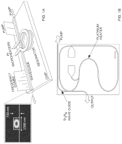
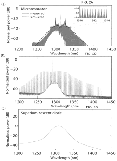
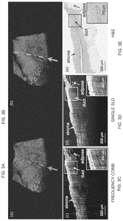
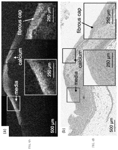
Microresonator-frequency-comb-based platform for clinical high-resolution optical coherence tomography
PatentActiveUS11859972B2
Innovation
- A microresonator-frequency-comb-based platform using high-Q silicon nitride resonators and distributed feedback lasers generates broadband frequency combs, overcoming the bandwidth-power trade-off and enabling sub-micrometer axial resolution and deeper tissue penetration, compatible with standard OCT systems.
Microelectromechanical resonator and method for fabrication
PatentActiveUS7652547B1
Innovation
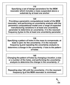
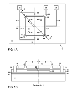
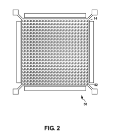
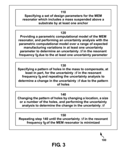
- A method involving the specification of design parameters for MEM resonators, including a mass suspended above a substrate by anchors, with a pattern of holes designed to compensate for manufacturing uncertainties through parametric computational modeling and iterative optimization to minimize the uncertainty in resonant frequency.
Material Science Advancements for Microcomb Fabrication
Material science has emerged as a critical frontier in advancing microcomb resonator fabrication technologies. Recent breakthroughs in material engineering have significantly impacted manufacturing yields by providing enhanced control over optical, mechanical, and thermal properties. Silicon nitride (Si3N4) remains the gold standard material for integrated photonic microresonators due to its wide transparency window, high refractive index, and negligible nonlinear absorption in the telecommunications band.
The development of ultra-low-loss Si3N4 films with reduced hydrogen content has been transformative for microcomb fabrication. These advanced films demonstrate propagation losses below 1 dB/m, representing a substantial improvement over previous generations. This advancement directly correlates with higher Q-factors in resonators, which is essential for achieving the threshold conditions necessary for Kerr comb generation at reasonable power levels.
Novel deposition techniques have revolutionized material consistency across wafers. Plasma-enhanced chemical vapor deposition (PECVD) with optimized precursor ratios and carefully controlled chamber conditions has enabled the production of films with stress profiles that minimize waveguide deformation. Additionally, atomic layer deposition (ALD) techniques have provided unprecedented precision in creating ultra-thin cladding layers with atomically smooth interfaces, reducing scattering losses significantly.
Hybrid material systems represent another promising direction, combining the benefits of different materials to overcome individual limitations. For instance, lithium niobate on insulator (LNOI) platforms integrate the strong electro-optic properties of lithium niobate with the low-loss characteristics of silica substrates, enabling active tuning capabilities while maintaining high Q-factors necessary for efficient comb generation.
Surface passivation technologies have addressed one of the most persistent yield challenges in microcomb fabrication. Advanced treatments using hydrogen annealing and silicon dioxide capping layers have demonstrated remarkable success in neutralizing surface states that contribute to absorption losses. These treatments have been shown to improve Q-factors by up to 40% in some resonator designs, directly translating to higher manufacturing yields.
The introduction of stress-engineered films represents another significant advancement. By precisely controlling film deposition parameters, researchers have developed methods to induce beneficial stress profiles that can compensate for fabrication-induced geometric variations. This approach has proven particularly valuable for maintaining phase-matching conditions across entire wafers, resulting in more consistent comb generation thresholds and spectral characteristics among fabricated devices.
Quality Control and Testing Methodologies
Quality control and testing methodologies represent critical components in achieving high manufacturing yields for microcomb resonator fabrication. The implementation of rigorous inspection protocols throughout the production process significantly impacts final device performance and consistency. Optical characterization techniques, including transmission spectroscopy and resonance linewidth measurements, serve as primary methods for evaluating resonator quality factors and coupling efficiencies. These measurements provide essential feedback on fabrication precision and material quality.
Advanced metrology systems employing atomic force microscopy (AFM) and scanning electron microscopy (SEM) enable sub-nanometer surface roughness assessment, which directly correlates with scattering losses in the finished resonators. Statistical process control (SPC) charts tracking key parameters such as waveguide dimensions, gap spacing, and material deposition rates help identify process drift before it impacts yield. Manufacturers leading the field have established tolerance thresholds based on extensive empirical testing, typically maintaining dimensional variations below ±5nm for critical features.
Non-destructive testing methods have gained prominence, with infrared thermography detecting subsurface defects and stress patterns that may lead to performance degradation. Wafer-level automated optical inspection systems capable of identifying particles, scratches, and lithographic errors have reduced defect escape rates by approximately 85% compared to manual inspection processes. These systems generate substantial datasets that, when analyzed through machine learning algorithms, reveal subtle correlations between process parameters and device performance.
In-line monitoring techniques measuring real-time process variables such as temperature uniformity, gas flow stability, and plasma characteristics provide immediate feedback for process adjustment. The integration of these monitoring systems with automated process control has demonstrated yield improvements of 15-30% in industrial settings. Standardized test structures incorporated into production wafers serve as process monitors, allowing rapid assessment of critical parameters without sacrificing production devices.
Functional testing protocols evaluating frequency comb generation, threshold power requirements, and spectral characteristics represent the final verification stage. These tests typically employ standardized optical coupling setups with automated alignment systems to ensure measurement consistency. Leading manufacturers have established comprehensive test databases correlating fabrication parameters with functional performance metrics, creating powerful predictive models for yield optimization. The implementation of statistical design of experiments (DOE) methodologies has proven particularly effective in identifying key process sensitivities and establishing robust operating windows.
Unlock deeper insights with Patsnap Eureka Quick Research — get a full tech report to explore trends and direct your research. Try now!
Generate Your Research Report Instantly with AI Agent
Supercharge your innovation with Patsnap Eureka AI Agent Platform!