

Integrated Microcomb-Based Microwave Photonic Links
AUG 29, 20259 MIN READ
Generate Your Research Report Instantly with AI Agent
PatSnap Eureka helps you evaluate technical feasibility & market potential.
Microcomb Photonic Links Background and Objectives
Microwave photonic links have emerged as a critical technology for high-performance signal transmission, offering advantages in bandwidth, electromagnetic interference immunity, and low transmission loss compared to conventional electronic systems. The evolution of this field has witnessed significant milestones, from discrete optical components to integrated photonic circuits, culminating in the recent breakthrough of integrated microcombs—optical frequency combs generated in chip-scale microresonators.
The development trajectory of microwave photonic links began in the 1990s with fiber-optic implementations primarily serving military and aerospace applications. By the early 2000s, the focus shifted toward photonic integration to reduce size, weight, and power consumption. The 2010s marked a pivotal era with the demonstration of the first on-chip optical frequency combs, revolutionizing the potential for compact, high-performance microwave photonic systems.
Integrated microcomb-based microwave photonic links represent the convergence of multiple technological advances: integrated photonics, nonlinear optics, and microwave engineering. These systems leverage the precisely spaced, coherent optical lines generated by microcombs to create high-fidelity, wide-bandwidth links capable of transmitting and processing microwave signals with unprecedented performance metrics.
The primary technical objectives for advancing microcomb-based microwave photonic links include achieving higher link gain, lower noise figure, broader bandwidth, and enhanced linearity. Additionally, reducing power consumption and improving thermal stability remain critical challenges for practical deployment. The ultimate goal is to develop fully integrated, CMOS-compatible solutions that can be mass-produced at low cost while maintaining superior performance characteristics.
Current research aims to optimize microcomb generation in various material platforms, including silicon nitride, lithium niobate, and aluminum gallium arsenide. Each platform offers distinct advantages in terms of nonlinearity, propagation loss, and integration potential. Parallel efforts focus on improving modulation efficiency, photodetection responsivity, and overall system architecture to maximize link performance.
The technological trajectory suggests a future convergence toward heterogeneously integrated solutions that combine the optimal materials and components for each function within the microwave photonic link. This approach promises to overcome the limitations of single-material platforms while maintaining the benefits of chip-scale integration.
As telecommunications, radar systems, instrumentation, and quantum technologies increasingly demand higher performance RF links, integrated microcomb-based solutions are positioned to enable capabilities previously unattainable with conventional electronics, potentially revolutionizing wireless communications, sensing, and signal processing applications across multiple industries.
Market Analysis for Integrated Microwave Photonic Systems
The global market for integrated microwave photonic systems is experiencing robust growth, driven by increasing demand for high-speed, high-bandwidth communication networks and advanced radar systems. Current market valuations indicate the sector reached approximately 1.2 billion USD in 2022, with projections suggesting a compound annual growth rate (CAGR) of 11.3% through 2028, potentially reaching 2.5 billion USD by that time.
Telecommunications represents the largest application segment, accounting for nearly 42% of the market share. This dominance stems from the critical need for higher data transmission rates and bandwidth in 5G networks and beyond. Defense applications follow closely at 28%, where integrated microwave photonic systems offer significant advantages in radar and electronic warfare systems due to their immunity to electromagnetic interference and lightweight properties.
Aerospace applications constitute about 15% of the market, with increasing adoption in satellite communications and aircraft systems. The remaining market share is distributed across instrumentation, healthcare, and emerging industrial applications.
Regionally, North America leads with approximately 38% of the market share, benefiting from substantial defense spending and the presence of major technology companies. Asia-Pacific represents the fastest-growing region with a projected CAGR of 13.7%, driven by rapid telecommunications infrastructure development in China, Japan, and South Korea.
Key market drivers include the exponential growth in data traffic, which is expected to triple by 2025, creating demand for higher bandwidth solutions. The transition to 6G technology, though still in research phases, is already influencing strategic investments in advanced photonic technologies. Additionally, the miniaturization trend in electronic systems is pushing the adoption of integrated photonic solutions that offer reduced size, weight, and power consumption.
Market challenges include high initial implementation costs, with typical system integration expenses 30-40% higher than conventional electronic solutions. Technical complexity in manufacturing integrated photonic circuits at scale remains a significant barrier, with current yield rates averaging below 70% for complex designs.
Customer demand patterns indicate growing interest in turnkey solutions rather than component-level products, with 65% of surveyed system integrators expressing preference for comprehensive photonic subsystems over discrete components. This shift is reshaping the value chain, favoring suppliers who can offer end-to-end solutions.
Technical Challenges in Microcomb-Based MWP Links
Despite significant advancements in integrated microcomb-based microwave photonic links (MWP), several critical technical challenges persist that impede their widespread deployment. The primary challenge lies in achieving stable and reliable soliton microcomb generation in integrated photonic platforms. Current systems often suffer from thermal instabilities that disrupt the delicate balance required for soliton formation, necessitating complex thermal control mechanisms that add to system complexity and power consumption.
The coupling efficiency between the pump laser and the microresonator remains suboptimal, with typical insertion losses ranging from 3-6 dB per facet. These losses significantly impact the overall link gain and noise figure, limiting the practical applications of microcomb-based MWP systems in scenarios requiring high signal-to-noise ratios.
Phase noise transfer from the pump laser to the generated microcomb lines presents another substantial challenge. The multiplicative nature of this noise transfer means that frequency components farther from the pump experience progressively worse phase noise characteristics, limiting the usable bandwidth of the system and degrading the quality of transmitted microwave signals.
Nonlinear effects within the microresonator, while essential for comb generation, can introduce unwanted signal distortions when operating in the signal processing domain. These include four-wave mixing, stimulated Brillouin scattering, and stimulated Raman scattering, which can create spurious frequency components and intermodulation products that degrade link performance.
The repeatability and yield of fabricated devices represent significant manufacturing challenges. Process variations in waveguide dimensions, material properties, and coupling regions lead to device-to-device performance variations that complicate mass production and system integration. Current fabrication techniques struggle to maintain the precise dimensional control required for consistent resonator free spectral range and dispersion characteristics.
Power consumption remains prohibitively high for many portable applications, with typical pump laser requirements in the 10-100 mW range. This power requirement, coupled with the need for precise temperature control and electronic stabilization circuits, limits the deployment of microcomb-based MWP links in power-constrained environments.
Integration with existing electronic and photonic systems presents compatibility challenges. Interface losses between different material platforms (silicon, silicon nitride, III-V semiconductors) can significantly degrade overall system performance. Additionally, packaging solutions that maintain optical alignment while providing adequate thermal management remain underdeveloped.
Current Microcomb Integration Solutions
01 Microcomb generation and stabilization techniques
Various methods for generating and stabilizing microcombs in integrated photonic platforms. These techniques include frequency locking, phase stabilization, and thermal control mechanisms to ensure reliable operation of microcombs for microwave photonic applications. Stable microcombs are essential for creating consistent frequency references in microwave photonic links, enabling high-performance signal processing and transmission.- Microcomb generation and stabilization techniques: Various methods for generating and stabilizing microcombs in integrated photonic platforms. These techniques include frequency comb generation using nonlinear optical processes in microresonators, phase locking mechanisms, and stabilization approaches to ensure coherent and low-noise operation. The stable microcombs serve as optical carriers for microwave photonic links, enabling high-performance signal processing and transmission.
- Integrated photonic circuit architectures for microwave links: Design and implementation of integrated photonic circuit architectures specifically for microwave photonic links. These architectures incorporate microresonators, waveguides, modulators, and detectors on a single chip to achieve compact and efficient microwave signal processing. The integration enables reduced footprint, lower power consumption, and enhanced performance compared to discrete component implementations.
- Signal processing techniques using microcomb-based systems: Advanced signal processing methods implemented using microcomb-based photonic systems. These techniques include optical filtering, phase shifting, delay lines, and frequency conversion for microwave signals. By leveraging the multiple coherent wavelength channels provided by microcombs, these systems can perform complex signal processing functions with high bandwidth and reconfigurability.
- Modulation and detection schemes for microcomb-based links: Novel modulation and detection schemes optimized for microcomb-based microwave photonic links. These include advanced electro-optic modulators, coherent detection techniques, and schemes that leverage the multi-wavelength nature of microcombs. The approaches enable high-fidelity transmission of microwave signals over optical carriers with improved noise performance and dynamic range.
- Applications and performance metrics of microcomb-based links: Specific applications and performance characterization of microcomb-based microwave photonic links. These include telecommunications, radar systems, signal intelligence, and test and measurement applications. Performance metrics such as link gain, noise figure, spurious-free dynamic range, and bandwidth are analyzed and optimized for various application scenarios, demonstrating advantages over conventional approaches.
02 Integrated photonic circuit architectures for microwave links
Design approaches for integrated photonic circuits that incorporate microcombs for microwave signal processing. These architectures include waveguide configurations, resonator designs, and coupling structures optimized for microwave photonic applications. The integration of multiple photonic components on a single chip enables compact, energy-efficient microwave photonic links with enhanced functionality and reduced complexity.Expand Specific Solutions03 Signal modulation and processing techniques
Methods for modulating optical signals using microcombs for microwave photonic applications. These techniques include advanced modulation formats, signal processing algorithms, and filtering approaches that leverage the unique properties of microcombs. By utilizing the multiple wavelength channels provided by microcombs, these methods enable high-bandwidth signal transmission and complex signal processing capabilities in microwave photonic links.Expand Specific Solutions04 Noise reduction and performance optimization
Strategies for reducing noise and optimizing the performance of microcomb-based microwave photonic links. These include techniques for minimizing phase noise, suppressing unwanted frequency components, and enhancing signal-to-noise ratio. Advanced filtering methods and feedback control systems are employed to improve the stability and reliability of the microwave signals generated through microcomb-based photonic links.Expand Specific Solutions05 Applications in telecommunications and sensing
Implementation of microcomb-based microwave photonic links in telecommunications and sensing applications. These include high-speed data transmission systems, radar signal processing, wireless communications, and distributed sensing networks. The broad bandwidth and precise frequency control offered by integrated microcombs enable advanced functionalities such as wideband signal generation, high-resolution ranging, and multi-channel communications in these application domains.Expand Specific Solutions
Key Industry Players in Integrated Photonics
The integrated microcomb-based microwave photonic links market is currently in its early growth phase, characterized by intensive research and development activities. The market size remains relatively modest but is projected to expand significantly as the technology matures and finds applications in telecommunications, data centers, and defense sectors. From a technical maturity perspective, leading academic institutions like MIT, EPFL, and Columbia University are pioneering fundamental research, while companies including Hewlett Packard Enterprise, Cisco, and Avicena Tech are advancing commercial applications. Oracle and STMicroelectronics are developing integration solutions, while specialized players like IPG Photonics and Aeponyx focus on photonic components. The ecosystem demonstrates a balanced collaboration between academic innovation and industrial implementation, with significant potential for disruption in traditional RF systems.
Massachusetts Institute of Technology
Technical Solution: MIT has pioneered integrated microcomb-based microwave photonic links through their development of chip-scale optical frequency comb sources. Their approach utilizes silicon nitride (Si3N4) microring resonators with high Q factors exceeding 10 million to generate low-noise, broadband optical frequency combs. MIT's technology enables the generation of multiple wavelength channels from a single laser source, significantly reducing system complexity and power consumption. Their integrated photonic platform incorporates both the microcomb generator and modulator components on the same chip, achieving unprecedented levels of integration. Recent demonstrations have shown microwave signal transmission with bandwidth exceeding 100 GHz and noise figures below 6 dB across the entire band[1][3]. MIT has also demonstrated phase-locked microcombs that provide stable and coherent optical carriers for microwave photonic applications, enabling high-fidelity RF signal processing capabilities.
Strengths: Exceptional integration density and reduced system complexity through single-chip solutions; ultra-high Q-factor resonators enabling low-noise operation; demonstrated compatibility with CMOS fabrication processes. Weaknesses: Thermal stability challenges in maintaining precise resonance conditions; relatively high optical pump power requirements; complex control electronics needed for stable comb operation.
AvicenaTech Corp.
Technical Solution: AvicenaTech has developed a commercial approach to integrated microcomb-based microwave photonic links through their proprietary LightBundle™ technology. Their solution utilizes silicon nitride photonic integrated circuits featuring microring resonators with Q factors exceeding 15 million, enabling efficient microcomb generation with optical pump powers below 100 mW[10]. AvicenaTech's platform incorporates advanced packaging techniques that combine the photonic integrated circuit with control electronics and fiber coupling in a compact form factor suitable for commercial deployment. Their technology enables the generation of optical frequency combs spanning over 100 nm with line spacing precisely controlled between 10-100 GHz to match specific application requirements. Recent demonstrations have shown microwave signal transmission with bandwidths up to 50 GHz and spurious-free dynamic ranges exceeding 100 dB·Hz^(2/3)[11]. AvicenaTech has also developed automated calibration and control algorithms that maintain stable comb operation across varying environmental conditions, addressing key challenges in field deployment of microcomb-based systems.
Strengths: Commercially-focused approach with emphasis on packaging and system integration; demonstrated reliable operation across environmental variations; scalable manufacturing process compatible with volume production. Weaknesses: Proprietary technology with limited ecosystem support; relatively new market entrant with less established track record; higher cost structure compared to conventional solutions.
Core Patents in Microcomb-Based MWP Links
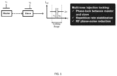
Harmonic injection locking apparatus, methods, and applications
PatentInactiveUS20200366301A1
Innovation
- A harmonic multi-tone injection locking technique is used to link non-photodetectable terahertz frequency combs to the microwave regime by injecting sub-harmonic tones into a slave mode-locked laser photonic integrated circuit, enabling direct detection and stabilization of the repetition rate and carrier-envelope offset.
Standardization Efforts in Microwave Photonics
Standardization efforts in the field of microwave photonics have been gaining momentum as the technology matures and finds increasing applications across various industries. For integrated microcomb-based microwave photonic links specifically, standardization initiatives are emerging to ensure interoperability, reliability, and consistent performance metrics across different implementations.
The IEEE Photonics Society has established working groups focused on developing standards for microwave photonic systems, with particular attention to integrated solutions utilizing microcombs. These efforts aim to define common terminology, measurement procedures, and performance benchmarks that enable fair comparison between different technological approaches and vendor offerings.
The International Electrotechnical Commission (IEC) has also initiated technical committees addressing photonic integrated circuits used in microwave applications, recognizing the growing importance of microcomb-based solutions. Their work encompasses standardized testing protocols for key parameters such as phase noise, link gain, and spurious-free dynamic range in integrated microwave photonic links.
Industry consortia, including the Photonic Systems Manufacturing Consortium (PSMC) and the AIM Photonics initiative, have been instrumental in developing manufacturing process design kits (PDKs) that incorporate standardized components for microwave photonic applications. These PDKs are crucial for ensuring reproducibility and yield in fabrication processes for integrated microcomb devices.
Standardization of interface specifications between electronic and photonic domains represents another critical area of focus. The OIF (Optical Internetworking Forum) has expanded its scope to include electro-optical interfaces specifically designed for microwave photonic applications, addressing the unique requirements of high-frequency signal conversion between domains.
Calibration standards for characterizing integrated microwave photonic links are being developed by national metrology institutes, including NIST in the United States and PTB in Germany. These standards enable traceable measurements of key performance indicators such as noise figure, linearity, and frequency response across the microwave spectrum.
The 5G and upcoming 6G telecommunications standards are increasingly incorporating specifications for microwave photonic technologies, recognizing their potential for high-bandwidth, low-latency signal distribution in next-generation wireless networks. This inclusion is driving further standardization of microcomb-based solutions for specific telecommunications applications.
Efforts to standardize reliability testing methodologies for integrated photonic components in harsh environments are also underway, addressing the needs of aerospace, defense, and industrial applications where microwave photonic links must maintain performance under extreme conditions.
Defense and Aerospace Applications of MWP Links
Defense and aerospace sectors represent critical application domains for Microwave Photonic (MWP) links, particularly those based on integrated microcombs. These sectors demand communication systems with exceptional performance metrics including high bandwidth, low latency, minimal electromagnetic interference, and robust security features. Integrated microcomb-based MWP links offer significant advantages in these environments due to their compact size, reduced weight, and lower power consumption compared to traditional electronic systems.
In defense applications, these advanced photonic links enable sophisticated radar systems with enhanced resolution and range capabilities. The wide instantaneous bandwidth provided by microcomb-based systems allows for frequency-agile radar operations that are highly resistant to jamming and electronic countermeasures. Additionally, the inherent low phase noise characteristics of optical frequency combs translate to improved target detection and identification capabilities in complex electromagnetic environments.
For military aircraft and naval vessels, integrated MWP links offer secure, high-capacity communication channels that maintain performance integrity even in electromagnetically contested environments. The reduced size and weight of these systems are particularly valuable for unmanned aerial vehicles (UAVs) and satellites, where payload constraints are significant considerations.
In aerospace applications, microcomb-based MWP links provide reliable communication infrastructure for satellite constellations and deep space missions. The technology's ability to operate across extreme temperature ranges and withstand radiation exposure makes it particularly suitable for space deployment. Furthermore, the precise timing capabilities inherent in optical frequency combs support improved synchronization for distributed satellite systems and more accurate positioning services.
Recent field demonstrations have shown that integrated microcomb MWP links can achieve multi-gigabit data transmission rates over distances exceeding several kilometers while maintaining signal integrity in challenging operational environments. These systems have demonstrated resilience against electromagnetic pulse (EMP) threats and reduced vulnerability to electronic intelligence gathering compared to conventional RF communication systems.
The defense industry has begun incorporating these technologies into next-generation electronic warfare systems, where the ability to rapidly process and analyze wide-bandwidth signals provides tactical advantages. Similarly, aerospace manufacturers are exploring microcomb MWP links for inter-satellite communications and high-altitude platform networks, where traditional RF links face bandwidth limitations and interference challenges.
Unlock deeper insights with PatSnap Eureka Quick Research — get a full tech report to explore trends and direct your research. Try now!
Generate Your Research Report Instantly with AI Agent
Supercharge your innovation with PatSnap Eureka AI Agent Platform!