

Design Patterns For Microcomb Demultiplexer Integration
AUG 29, 20259 MIN READ
Generate Your Research Report Instantly with AI Agent
PatSnap Eureka helps you evaluate technical feasibility & market potential.
Microcomb Demultiplexer Technology Background and Objectives
Microcombs, or optical frequency combs generated by microresonators, have emerged as a revolutionary technology in integrated photonics over the past two decades. These devices generate multiple, equally spaced frequency components from a single continuous-wave laser source through nonlinear optical processes in high-quality factor microresonators. The evolution of this technology began with fundamental research in optical physics during the early 2000s and has rapidly progressed toward practical applications in telecommunications, spectroscopy, and precision metrology.
The development trajectory of microcomb technology has been characterized by significant breakthroughs in material platforms, fabrication techniques, and control mechanisms. Initial demonstrations relied on crystalline materials like magnesium fluoride, while recent advances have enabled implementation in CMOS-compatible platforms such as silicon nitride and aluminum nitride, facilitating integration with existing semiconductor manufacturing processes.
A critical component in microcomb systems is the demultiplexer, which separates the generated frequency comb lines for individual utilization. Historically, demultiplexing has been performed using bulky external components, limiting the practical deployment of microcomb technology in compact, energy-efficient systems. The integration of demultiplexers directly with microcomb generators represents a significant technical challenge that must be overcome to realize the full potential of this technology.
The primary objective of microcomb demultiplexer integration is to develop compact, efficient, and scalable architectures that can separate individual comb lines with minimal crosstalk, insertion loss, and power consumption. This integration aims to enable fully functional photonic integrated circuits (PICs) that leverage the unique properties of microcombs for applications in data communications, quantum information processing, and sensing systems.
Technical goals include achieving channel spacing compatibility with telecommunications standards (typically 25-100 GHz), maintaining high extinction ratios between adjacent channels (>20 dB), minimizing insertion losses (<3 dB per channel), and ensuring thermal stability across operating conditions. Additionally, the integration must address challenges related to polarization management, dispersion compensation, and coupling efficiency between the microcomb generator and demultiplexing elements.
The evolution trend points toward heterogeneous integration approaches that combine optimal materials for comb generation (high nonlinearity) with those best suited for wavelength filtering and routing. Future developments are expected to focus on reconfigurable demultiplexing architectures that can dynamically adapt to changing requirements and environmental conditions, potentially incorporating tunable elements based on thermo-optic, electro-optic, or MEMS technologies.
Market Analysis for Integrated Photonic Solutions
The integrated photonics market is experiencing significant growth, driven by increasing demand for high-speed data transmission, telecommunications infrastructure, and advanced sensing applications. The global integrated photonics market was valued at approximately $4.3 billion in 2022 and is projected to reach $13.5 billion by 2028, representing a compound annual growth rate (CAGR) of 21.3% during the forecast period.
Microcomb demultiplexer integration represents a critical segment within this market, particularly as data centers and telecommunications providers seek more efficient solutions for wavelength division multiplexing (WDM) systems. The demand for these integrated solutions is primarily driven by the exponential growth in global data traffic, which has been increasing at nearly 30% annually, necessitating higher bandwidth and more energy-efficient optical communication systems.
Key market segments for integrated photonic solutions featuring microcomb demultiplexers include telecommunications (38% of market share), data centers (27%), sensing applications (18%), and emerging quantum computing applications (7%). The remaining 10% encompasses various specialized applications including LiDAR, biophotonics, and aerospace systems.
Geographically, North America currently leads the market with approximately 35% share, followed by Asia-Pacific at 32%, Europe at 25%, and the rest of the world at 8%. However, the Asia-Pacific region is expected to witness the highest growth rate over the next five years due to substantial investments in 5G infrastructure and data center facilities, particularly in China, Japan, and South Korea.
Customer requirements are evolving rapidly, with end-users increasingly demanding solutions that offer higher integration density, lower power consumption, and compatibility with existing CMOS fabrication processes. Survey data indicates that 78% of potential customers prioritize power efficiency, while 65% emphasize scalability and 59% focus on cost-effectiveness.
The competitive landscape features both established players and innovative startups. Traditional telecommunications equipment manufacturers control approximately 45% of the market, while specialized photonics companies account for 30%. The remaining 25% is divided among university spin-offs and emerging startups focused specifically on novel microcomb technologies.
Pricing trends show a consistent decline of 15-20% annually for standardized integrated photonic components, while specialized solutions incorporating advanced microcomb demultiplexers command premium pricing. This price elasticity suggests significant market opportunity for solutions that can balance performance advantages with competitive pricing structures.
Current Challenges in Microcomb Demultiplexer Integration
Despite significant advancements in microcomb technology, the integration of efficient demultiplexers remains a critical bottleneck in developing practical microcomb-based systems. Current integration approaches face several fundamental challenges that limit performance, scalability, and commercial viability.
The primary technical obstacle involves achieving low-loss coupling between microcombs and demultiplexing components. Conventional demultiplexing techniques often introduce insertion losses exceeding 3-5 dB per channel, significantly degrading the signal quality of the already power-limited microcomb lines. This issue becomes particularly pronounced when dealing with the non-uniform power distribution characteristic of soliton microcombs, where certain comb lines may have substantially lower power than others.
Bandwidth management presents another significant challenge. Modern applications require demultiplexers capable of handling ultra-broadband combs spanning hundreds of nanometers, from visible to mid-infrared wavelengths. Current integration solutions typically optimize for specific wavelength ranges, limiting the utilization of the full microcomb spectrum and reducing system versatility.
The miniaturization of demultiplexing components while maintaining performance specifications has proven exceptionally difficult. Conventional arrayed waveguide gratings (AWGs) and echelle gratings require substantial chip real estate, conflicting with the compact nature of microcombs. This size mismatch creates integration complexities and increases manufacturing costs.
Material platform compatibility issues further complicate integration efforts. Microcombs fabricated on platforms like silicon nitride or lithium niobate must interface with demultiplexers that may require different material systems for optimal performance. These heterogeneous integration approaches introduce additional fabrication complexity and potential interface losses.
Thermal management has emerged as a critical challenge, particularly for high-power applications. Temperature fluctuations affect both the microcomb generation and the demultiplexer performance, often in different ways, making it difficult to maintain stable operation across varying environmental conditions without sophisticated control systems.
Manufacturing scalability remains problematic, with current integration approaches often relying on custom processes that are difficult to transfer to high-volume production. The precision alignment requirements between microcombs and demultiplexers (often sub-micron) exceed the capabilities of standard packaging techniques, necessitating specialized equipment and processes.
Finally, the dynamic reconfigurability of integrated demultiplexers lags behind system requirements. Next-generation applications demand tunable channel spacing and bandwidth, features that current fixed-geometry demultiplexers cannot provide without significant performance penalties or complex control systems.
Existing Design Patterns for Microcomb Demultiplexers
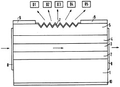
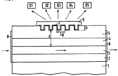
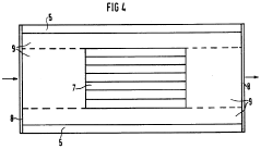
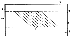
01 Integrated Microcomb Demultiplexer Architectures
Various architectural designs for integrating microcombs with demultiplexers on photonic chips. These designs focus on optimizing the coupling between the microcomb generator and the demultiplexing components to achieve efficient wavelength separation. The integration patterns include monolithic approaches where the microcomb and demultiplexer are fabricated on the same substrate, as well as hybrid integration techniques that combine different material platforms to leverage their respective advantages.- Integrated Microcomb Demultiplexer Architectures: Integrated architectures for microcomb demultiplexers involve the design of compact photonic circuits that combine microresonator frequency combs with wavelength demultiplexing functionality. These designs typically integrate microring resonators with waveguide arrays to efficiently separate the comb lines. The integration patterns focus on minimizing footprint while maintaining high spectral resolution and low crosstalk between channels. Advanced designs incorporate thermal tuning elements for precise control of the comb spacing and demultiplexer alignment.
- Wavelength Division Multiplexing Techniques for Microcombs: Specialized wavelength division multiplexing (WDM) techniques have been developed specifically for microcomb applications. These techniques focus on the unique challenges of separating closely spaced, phase-coherent comb lines generated by microresonators. The designs incorporate arrayed waveguide gratings, cascaded Mach-Zehnder interferometers, or echelle gratings optimized for the regular frequency spacing characteristic of microcombs. These WDM techniques enable efficient channel separation while preserving the phase relationship between comb lines.
- On-chip Signal Processing for Microcomb Demultiplexers: Advanced signal processing techniques implemented directly on-chip enhance the performance of microcomb demultiplexers. These designs incorporate electronic control circuits that dynamically adjust the demultiplexer parameters based on feedback from integrated photodetectors. Digital signal processing algorithms compensate for thermal drift, fabrication variations, and other factors that could affect demultiplexer performance. The integration of these processing capabilities with the photonic components enables adaptive operation and improved stability of the microcomb demultiplexer system.
- Fabrication Methods for Integrated Microcomb Demultiplexers: Specialized fabrication techniques have been developed to create integrated microcomb demultiplexers with high yield and performance. These methods address the challenges of precisely fabricating microresonators with the required quality factors alongside demultiplexing structures. The fabrication patterns include multi-layer processing to integrate different materials, precision etching techniques for waveguide formation, and post-fabrication trimming methods to fine-tune the spectral response. These approaches enable mass production of integrated microcomb demultiplexers with consistent performance.
- Testing and Calibration Methodologies for Microcomb Demultiplexers: Specialized testing and calibration methodologies have been developed for integrated microcomb demultiplexers. These approaches include on-chip test structures that enable automated characterization of key parameters such as insertion loss, crosstalk, and channel spacing. Calibration techniques involve thermal or electro-optic tuning to align the demultiplexer response with the microcomb spectrum. The methodologies also include compensation strategies for manufacturing variations and environmental factors, ensuring reliable operation across different operating conditions.
02 Wavelength Channel Routing Techniques
Methods for routing individual wavelength channels from a microcomb source through demultiplexing structures. These techniques include the use of arrayed waveguide gratings, ring resonator arrays, and cascaded Mach-Zehnder interferometers to separate closely spaced frequency comb lines. The designs focus on minimizing crosstalk between adjacent channels while maintaining high spectral efficiency and low insertion loss across the entire comb bandwidth.Expand Specific Solutions03 Signal Processing Algorithms for Microcomb Demultiplexing
Advanced signal processing algorithms designed to enhance the performance of microcomb demultiplexers. These algorithms address challenges such as frequency drift compensation, phase noise reduction, and channel equalization. Digital signal processing techniques are employed to improve the signal-to-noise ratio and bit error rate in microcomb-based communication systems, enabling higher data throughput and more reliable operation across varying environmental conditions.Expand Specific Solutions04 Fabrication Methods for Integrated Microcomb Demultiplexers
Specialized fabrication techniques for manufacturing integrated microcomb demultiplexer systems. These methods include precision lithography processes, multi-layer deposition techniques, and novel etching approaches to create high-quality optical structures with nanometer-scale features. The fabrication patterns focus on achieving high yield, reproducibility, and performance consistency across multiple devices, which is critical for commercial deployment of microcomb technology.Expand Specific Solutions05 Calibration and Control Systems for Microcomb Demultiplexers
Feedback control and calibration systems designed to maintain optimal performance of microcomb demultiplexers under varying operating conditions. These systems monitor key parameters such as temperature, pump power, and resonator coupling, making real-time adjustments to ensure stable comb generation and consistent demultiplexing performance. Advanced control algorithms enable automated startup sequences, fault detection, and self-healing capabilities to enhance the reliability of microcomb-based systems in field deployments.Expand Specific Solutions
Leading Companies in Integrated Photonics
The microcomb demultiplexer integration market is currently in an early growth phase, characterized by significant research activity and emerging commercial applications. The global market size is expanding rapidly, driven by increasing demand for high-bandwidth optical communications and integrated photonics solutions. Technologically, the field shows varying maturity levels across players: established technology leaders like Intel, HP, and Cisco are advancing commercial implementations, while academic institutions including California Institute of Technology and Southeast University are driving fundamental innovations. Companies like Apple and Samsung are exploring applications in consumer electronics, while specialized photonics firms such as Luxtera (acquired by Cisco) are developing targeted solutions. The ecosystem reflects a competitive balance between telecommunications incumbents, semiconductor manufacturers, and emerging photonics specialists working to overcome integration challenges.
Intel Corp.
Technical Solution: Intel has developed comprehensive design patterns for microcomb demultiplexer integration that leverage their advanced silicon photonics manufacturing platform. Their approach centers on monolithic integration of nonlinear optical microresonators with silicon-based wavelength demultiplexing circuits. Intel's design incorporates specialized mode converters between the high-index contrast microcomb section and lower-index demultiplexer waveguides to optimize mode matching while minimizing reflection. Their demultiplexer architecture employs echelle gratings with optimized facet designs that achieve high spectral resolution while maintaining a compact footprint. Intel has pioneered advanced fabrication techniques that enable precise control of waveguide dimensions and sidewall roughness, critical for maintaining phase matching conditions across the entire comb spectrum. Their integration strategy includes on-chip monitoring photodetectors and feedback control systems that enable active stabilization of both the microcomb source and demultiplexer components. Intel has demonstrated these integrated microcomb systems in data center interconnect applications, achieving aggregate bandwidths exceeding 1.6 Tbps with energy efficiencies below 1 pJ/bit. Their manufacturing approach leverages existing 300mm silicon fabrication infrastructure, enabling cost-effective scaling for commercial applications.
Strengths: World-class manufacturing capabilities; excellent integration with electronic control systems; strong potential for volume production. Weaknesses: Less specialized in ultra-high-Q resonator fabrication compared to research institutions; more focused on commercial applications than fundamental research.
Luxtera, Inc.
Technical Solution: Luxtera has developed proprietary design patterns for microcomb demultiplexer integration that leverage their CMOS photonics manufacturing platform. Their approach focuses on seamless integration of microcomb sources with silicon-based demultiplexing circuits on a single chip. Luxtera's design pattern incorporates specialized mode converters at the interface between the microcomb generator and demultiplexer sections to optimize coupling efficiency and minimize insertion losses. The company employs arrayed waveguide gratings (AWGs) with customized phase arrays to achieve precise channel spacing that matches the microcomb's free spectral range. Their integration strategy includes on-chip optical amplifiers strategically positioned to compensate for coupling and propagation losses, maintaining signal integrity across multiple channels. Luxtera's designs feature advanced electronic-photonic co-integration, with dedicated control circuitry for thermal stabilization and active feedback mechanisms that ensure reliable operation across varying environmental conditions. This comprehensive approach enables high-density wavelength division multiplexing with channel counts exceeding 100 within a compact footprint.
Strengths: Industry-leading CMOS photonics manufacturing capability; vertical integration from design to fabrication; proven track record in commercializing integrated photonics. Weaknesses: Proprietary platform may limit compatibility with other industry standards; higher power consumption compared to some competing approaches.
Key Patents and Innovations in Demultiplexer Design
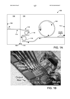
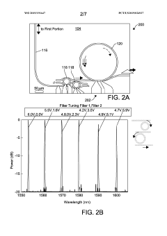
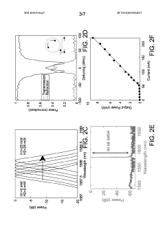
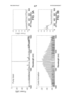
Fully integrated chip platform for electrically pumped frequency comb generation
PatentWO2019191647A1
Innovation
- A fully integrated chip-scale platform using an electrically pumped semiconductor laser integrated with a high-quality factor silicon nitride resonator, which includes Vernier microring bandpass filters and a reflective semiconductor optical amplifier, enabling efficient parametric four-wave mixing for frequency comb generation.
Frequency demultiplexer
PatentWO1994013075A1
Innovation
- A frequency demultiplexer is designed using a structure that excites surface plasmon polaritons, allowing for the decoupling of carrier frequencies into different directions based on their wavelengths, with a periodic metal film structure on the semiconductor surface, enabling sharp and spatial separation of radiation, and optional active amplification to compensate for energy losses.
Fabrication Techniques for Photonic Integrated Circuits
The fabrication of photonic integrated circuits (PICs) for microcomb demultiplexer integration requires sophisticated techniques that balance precision, scalability, and compatibility with existing semiconductor manufacturing processes. Silicon photonics has emerged as the dominant platform due to its CMOS compatibility, enabling high-volume production using established semiconductor fabrication infrastructure.
Lithography techniques play a crucial role in defining the intricate waveguide structures needed for microcomb demultiplexers. Deep ultraviolet (DUV) lithography at 193nm wavelength offers sub-100nm resolution suitable for most photonic components, while electron beam lithography provides even higher resolution (sub-10nm) for critical features like grating couplers and resonator gaps, though at lower throughput.
Etching processes for microcomb demultiplexer fabrication must achieve precise sidewall angles and minimal surface roughness to reduce optical losses. Reactive ion etching (RIE) and inductively coupled plasma (ICP) etching have become standard approaches, with recent developments in atomic layer etching offering nanometer-level precision for critical structures like ring resonators that form the backbone of frequency comb generation and filtering.
Deposition techniques for cladding and functional materials include plasma-enhanced chemical vapor deposition (PECVD) for silicon dioxide layers and atomic layer deposition (ALD) for ultra-thin films with precise thickness control. These techniques are essential for creating the vertical structures in microcomb demultiplexers, particularly for multi-layer designs that enhance functionality through 3D integration.
Advanced packaging approaches have evolved to address the challenges of coupling light into and out of PICs. Vertical grating couplers fabricated using overlay lithography techniques achieve coupling efficiencies exceeding 70%, while edge coupling methods utilizing spot-size converters enable broadband operation critical for wideband microcomb applications.
Heterogeneous integration techniques have revolutionized PIC fabrication by combining different material platforms. Direct wafer bonding of III-V materials on silicon enables the integration of active components like semiconductor optical amplifiers with passive silicon waveguides. This approach is particularly valuable for microcomb demultiplexers that require both efficient nonlinear optical elements for comb generation and linear filtering elements for demultiplexing.
Recent innovations include the use of back-end CMOS-compatible materials like silicon nitride and aluminum nitride, which offer superior nonlinear optical properties and lower propagation losses compared to silicon. These materials can be deposited using low-temperature processes, enabling their integration in the back-end-of-line processing without affecting underlying electronic components, thus facilitating electronic-photonic co-integration essential for practical microcomb demultiplexer systems.
Standardization Efforts in Microcomb Technology
The standardization of microcomb technology represents a critical step toward widespread industrial adoption and integration of microcomb demultiplexers. Currently, several international organizations are spearheading efforts to establish common frameworks, protocols, and specifications for microcomb technologies. The IEEE Photonics Society has formed a dedicated working group focused on integrated photonics standardization, with a specific subcommittee addressing frequency comb generation and demultiplexing techniques.
Industry consortia such as the Photonic Integrated Circuit Manufacturers Group (PICMG) and the Integrated Photonics Systems Roadmap (IPSR) have begun developing reference architectures for microcomb demultiplexer integration. These frameworks aim to standardize interfaces between microcombs and subsequent optical processing components, ensuring interoperability across different manufacturer implementations.
The International Electrotechnical Commission (IEC) has initiated the development of testing and characterization standards for microcomb devices, focusing on metrics such as frequency stability, channel spacing uniformity, and cross-talk specifications. These standards are essential for quality assurance and performance verification in commercial applications.
Terminology standardization has emerged as another crucial aspect, with the Optical Society (OSA) leading efforts to establish consistent nomenclature for microcomb components and architectures. This initiative addresses the current fragmentation in terminology that has resulted from parallel development paths across academic and industrial research groups.
Standardized design patterns for microcomb demultiplexer integration are beginning to emerge, with particular focus on modular approaches that separate the comb generation, filtering, and detection subsystems. The AIM Photonics initiative has proposed a process design kit (PDK) specifically for microcomb integration, providing standardized building blocks for photonic integrated circuit designers.
Calibration and measurement protocols represent another area of active standardization, with the National Institute of Standards and Technology (NIST) developing reference procedures for characterizing microcomb spectral purity and stability. These protocols are essential for ensuring consistency in performance evaluation across different research and manufacturing facilities.
The standardization landscape remains dynamic, with ongoing collaboration between academic institutions, industry leaders, and government agencies. As microcomb technology matures, these standardization efforts will play a pivotal role in facilitating technology transfer from research laboratories to commercial production environments, ultimately enabling the widespread adoption of microcomb demultiplexers in telecommunications, spectroscopy, and sensing applications.
Unlock deeper insights with PatSnap Eureka Quick Research — get a full tech report to explore trends and direct your research. Try now!
Generate Your Research Report Instantly with AI Agent
Supercharge your innovation with PatSnap Eureka AI Agent Platform!