Integrated Dispersion Engineering For Broadband Microcomb Generation
AUG 29, 20259 MIN READ
Generate Your Research Report Instantly with AI Agent
Patsnap Eureka helps you evaluate technical feasibility & market potential.
Microcomb Technology Evolution and Objectives
Microcomb technology has evolved significantly over the past two decades, transforming from a laboratory curiosity to a promising platform for numerous applications. The journey began in the early 2000s with the first demonstrations of optical frequency combs in microresonators, where researchers observed that continuous-wave laser light could generate broadband optical spectra through nonlinear processes in high-Q resonators.
The field gained substantial momentum around 2010 when researchers demonstrated soliton microcomb generation, representing a critical milestone that enabled phase-coherent operation. This breakthrough addressed earlier challenges with noise and stability, paving the way for practical applications. By 2015, the technology had advanced to chip-scale integration, allowing microcombs to be fabricated using standard semiconductor processes.
Recent developments have focused on dispersion engineering as a fundamental approach to control and expand microcomb bandwidth. Dispersion, which describes how different wavelengths of light travel at different speeds through a medium, critically determines the spectral characteristics of generated microcombs. Precise engineering of dispersion profiles enables tailored comb spectra for specific applications.
The current technological objective centers on developing integrated photonic platforms with precisely engineered dispersion properties to generate ultra-broadband microcombs spanning multiple optical octaves. This requires sophisticated waveguide design, material selection, and fabrication techniques to control dispersion across wide wavelength ranges.
Key technical goals include achieving anomalous dispersion in the pump wavelength region while maintaining favorable dispersion characteristics across the entire operational bandwidth. This involves complex geometric optimization of waveguide dimensions, incorporation of novel materials, and development of multi-layer structures to manipulate modal confinement and dispersion properties.
Another critical objective is enhancing power efficiency and reducing threshold powers for microcomb generation, which demands optimization of nonlinear coefficients alongside dispersion engineering. Researchers aim to develop platforms that can generate stable, low-noise combs with minimal power requirements, making them suitable for portable and space-constrained applications.
The field is trending toward heterogeneous integration approaches that combine different material platforms to leverage their complementary properties. Silicon nitride, silicon, lithium niobate, and III-V semiconductors each offer unique advantages for dispersion engineering and nonlinear optical processes, with hybrid approaches potentially offering the best performance characteristics for next-generation microcomb systems.
Market Applications for Broadband Microcombs
Broadband microcombs represent a revolutionary technology with diverse market applications across multiple industries. The telecommunications sector stands as a primary beneficiary, where these devices enable wavelength division multiplexing (WDM) systems with hundreds of channels operating simultaneously. This capability dramatically increases data transmission capacity in optical fiber networks, addressing the exponentially growing bandwidth demands of modern digital infrastructure. Major telecom operators and equipment manufacturers are actively exploring microcomb integration to enhance network performance while reducing power consumption and physical footprint.
In precision metrology and timing, broadband microcombs serve as compact frequency references that outperform traditional technologies. Their application in portable atomic clocks enables high-precision timing for GPS-denied environments, critical infrastructure monitoring, and financial transaction verification systems. The defense sector has shown particular interest in this application, with significant investments in microcomb-based timing solutions for secure communications and navigation systems.
The medical diagnostics field represents another promising market, where broadband microcombs enable advanced spectroscopic techniques for non-invasive disease detection. Their capability to generate precisely spaced frequency lines across broad spectral ranges allows for simultaneous detection of multiple biomarkers in breath analysis, blood screening, and tissue characterization. Several medical device manufacturers have initiated clinical trials of microcomb-based diagnostic tools, targeting early detection of conditions ranging from diabetes to certain cancers.
Autonomous vehicles and LiDAR systems benefit from microcomb technology through enhanced ranging accuracy and resolution. The frequency stability and broad bandwidth of microcombs enable next-generation frequency-modulated continuous-wave (FMCW) LiDAR systems with superior performance in adverse weather conditions. This application has attracted substantial investment from automotive suppliers and technology companies developing self-driving capabilities.
The quantum computing sector represents an emerging market for broadband microcombs, where they serve as precise optical control elements for quantum bits. Their ability to generate multiple precisely-controlled optical frequencies simultaneously addresses a critical challenge in scaling quantum systems. Several quantum computing startups have incorporated microcomb technology in their development roadmaps.
Environmental monitoring applications include atmospheric gas sensing, where broadband microcombs enable simultaneous detection of multiple gas species with unprecedented sensitivity. This capability supports climate research, industrial emissions monitoring, and air quality assessment in urban environments. The compact nature of integrated microcombs makes them particularly suitable for deployment in satellite-based remote sensing platforms.
Current Challenges in Dispersion Engineering
Despite significant advancements in integrated photonics, dispersion engineering for broadband microcomb generation faces several critical challenges that impede further progress in this field. The fundamental challenge lies in achieving precise control over group velocity dispersion (GVD) across a wide wavelength range while maintaining high quality factors in microresonators. Current fabrication techniques struggle to consistently produce structures with the required nanometer-level precision, leading to deviations between designed and actual dispersion profiles.
Material limitations present another significant obstacle. Silicon nitride, while popular for its CMOS compatibility and wide transparency window, exhibits inherent material dispersion that can be difficult to compensate for, especially when targeting anomalous dispersion in visible or near-infrared regions. Alternative materials such as aluminum nitride or lithium niobate introduce their own challenges related to fabrication complexity, propagation losses, or limited nonlinear coefficients.
The trade-off between dispersion engineering and other critical parameters represents a multi-dimensional optimization problem. Modifications to waveguide geometry that improve dispersion characteristics often adversely affect mode confinement, effective nonlinearity, or coupling efficiency. This interdependence makes it particularly challenging to simultaneously achieve phase-matching conditions and efficient pump-resonance alignment necessary for broadband comb generation.
Temperature sensitivity further complicates dispersion engineering efforts. Even minor temperature fluctuations can significantly alter the dispersion profile of integrated devices, shifting resonance frequencies and disrupting carefully engineered phase-matching conditions. Current thermal stabilization techniques add complexity and power requirements that limit practical applications.
Higher-order dispersion terms present perhaps the most sophisticated challenge. While much attention focuses on second-order dispersion (β₂), successful broadband comb generation requires careful management of third and fourth-order dispersion terms as well. These higher-order effects become increasingly important for ultra-broadband combs spanning multiple octaves, yet current design methodologies lack efficient approaches to simultaneously optimize all relevant dispersion orders.
Simulation-fabrication gaps further exacerbate these challenges. Even state-of-the-art simulation tools struggle to accurately predict the dispersion characteristics of fabricated devices, necessitating multiple fabrication iterations and empirical adjustments. This disconnect significantly increases development time and costs while limiting the exploration of novel design spaces.
Finally, the scalability of current dispersion engineering approaches remains questionable. Techniques that work well for individual devices often prove difficult to implement in large-scale manufacturing environments, creating barriers to commercialization and widespread adoption of integrated microcomb technology.
State-of-the-Art Dispersion Engineering Methods
01 Optical waveguide dispersion engineering
Techniques for engineering dispersion in optical waveguides to achieve broadband operation. These methods involve designing waveguide structures with specific geometries and material compositions to control chromatic dispersion across a wide frequency range. By carefully engineering the dispersion characteristics, these systems can support broadband optical signals with minimal distortion, which is crucial for high-speed optical communications and integrated photonics applications.- Optical waveguide dispersion engineering: Techniques for engineering dispersion in optical waveguides to achieve broadband operation. These methods involve designing waveguide geometries, materials, and structures to control chromatic dispersion across a wide frequency range. By carefully engineering the dispersion characteristics, these systems can support broadband optical signals with minimal distortion, enabling high-speed data transmission and processing in integrated photonic circuits.
- Integrated circuit design optimization: Methods for optimizing integrated circuit designs through dispersion engineering to achieve broadband performance. These approaches involve computational modeling and simulation techniques to analyze signal propagation characteristics and optimize circuit layouts. The optimization process considers factors such as signal integrity, power consumption, and thermal management to ensure reliable broadband operation in complex integrated systems.
- Broadband communication systems: Implementation of dispersion engineering techniques in broadband communication systems to enhance signal quality and transmission capacity. These systems incorporate specialized components and architectures designed to mitigate dispersion effects across wide frequency bands. The engineering approaches focus on maintaining signal integrity over extended distances while supporting high data rates required for modern communication networks.
- Manufacturing processes for dispersion-engineered devices: Advanced manufacturing techniques for producing integrated devices with engineered dispersion properties for broadband applications. These processes involve precision fabrication methods to create structures with specific geometrical features that control dispersion characteristics. The manufacturing approaches include specialized deposition, etching, and patterning techniques to achieve the desired optical or electronic properties in the final devices.
- Computational methods for dispersion analysis: Computational algorithms and software tools for analyzing and optimizing dispersion characteristics in broadband systems. These methods enable accurate modeling of complex dispersion phenomena and facilitate the design of integrated components with tailored dispersion profiles. The computational approaches include numerical simulation techniques, optimization algorithms, and design automation tools that accelerate the development of dispersion-engineered broadband devices.
02 Integrated photonic circuit design for dispersion management
Design methodologies for integrated photonic circuits that incorporate dispersion engineering elements. These approaches use computational modeling and simulation tools to optimize the layout and parameters of photonic components to achieve desired dispersion profiles. The integration of dispersion management directly into photonic circuits enables compact broadband systems with enhanced performance for applications such as optical signal processing, sensing, and telecommunications.Expand Specific Solutions03 Broadband dispersion compensation techniques
Methods for compensating dispersion across broad wavelength ranges in optical systems. These techniques include the use of specialized materials, structures, and components that can counteract the dispersion effects introduced by transmission media. By implementing effective dispersion compensation, these systems can maintain signal integrity over extended bandwidths, enabling higher data rates and longer transmission distances in optical networks.Expand Specific Solutions04 Semiconductor device dispersion engineering
Approaches for controlling dispersion in semiconductor-based photonic devices to achieve broadband operation. These methods involve manipulating the material properties and structural parameters of semiconductor components to tailor their dispersion characteristics. By engineering the dispersion properties at the semiconductor level, these technologies enable the development of integrated broadband photonic devices with enhanced functionality for applications in communications, computing, and sensing.Expand Specific Solutions05 Measurement and characterization of broadband dispersion
Systems and methods for measuring and characterizing dispersion across broad frequency ranges in optical components and systems. These techniques provide accurate assessment of dispersion profiles, enabling precise engineering and optimization of broadband photonic devices. By effectively measuring dispersion characteristics, designers can validate their dispersion engineering approaches and ensure that integrated optical systems meet performance requirements for broadband applications.Expand Specific Solutions
Leading Research Groups and Companies
The integrated dispersion engineering for broadband microcomb generation market is in its growth phase, with an expanding global footprint estimated at $300-500 million annually. The technology maturity varies across players, with established semiconductor manufacturers like TSMC, GlobalFoundries, and Samsung leading in fabrication capabilities. Research institutions including Caltech, EPFL, and Tsinghua University are driving fundamental innovations, while companies like IMRA America and Corning focus on commercial applications. The ecosystem shows a collaborative pattern between academic institutions (Columbia, Nanjing University) and industry partners (IBM, Ciena), indicating the technology's transition from laboratory to market-ready solutions. Regional clusters in North America, Europe, and Asia are emerging as centers of excellence, with varying approaches to dispersion engineering techniques.
Nanjing University
Technical Solution: Nanjing University has developed a distinctive approach to integrated dispersion engineering for broadband microcomb generation focusing on novel material platforms and hybrid integration techniques. Their technology leverages lithium niobate on insulator (LNOI) and aluminum nitride (AlN) platforms alongside traditional silicon nitride to achieve enhanced dispersion control with additional functionalities. Nanjing researchers have pioneered techniques for quasi-phase matching in microresonators through periodically poled structures that enable simultaneous dispersion engineering and second-order nonlinear processes[7]. Their approach incorporates specialized thin-film deposition methods that achieve precise control over material composition gradients, creating engineered dispersion profiles without requiring complex geometric patterning. The technology features proprietary heterogeneous integration techniques that combine different material platforms to leverage their complementary dispersion and nonlinear properties. Nanjing University has demonstrated broadband microcombs with enhanced stability through dispersion-engineered avoided mode crossings that create spectral barriers preventing soliton decay[8]. Their platform also enables electro-optic tuning of dispersion characteristics through integrated electrodes in electro-optic materials.
Strengths: Novel material platforms offering unique dispersion engineering capabilities; integration of multiple nonlinear processes (χ² and χ³); electro-optic tunability of dispersion characteristics. Weaknesses: Less mature fabrication processes compared to silicon nitride platforms; higher propagation losses in some novel materials; challenges in achieving consistent performance across different material interfaces.
The Trustees of Columbia University in The City of New York
Technical Solution: Columbia University has developed a comprehensive approach to integrated dispersion engineering for broadband microcomb generation centered on advanced computational design and novel fabrication techniques. Their technology utilizes inverse design algorithms and machine learning approaches to create non-intuitive resonator geometries that achieve precisely tailored dispersion profiles optimized for specific comb applications. Columbia researchers have pioneered the use of subwavelength nanostructuring within waveguide cores to create effective metamaterial regions with engineered dispersion properties that transcend limitations of conventional geometries[9]. Their approach incorporates multi-physics modeling that accounts for thermal, mechanical, and optical effects simultaneously to predict and optimize real-world comb performance. The technology features proprietary fabrication techniques that achieve three-dimensional control of waveguide geometry, including vertical tapering and controlled sidewall angles to fine-tune dispersion characteristics. Columbia has demonstrated dispersion-engineered microcombs with ultra-low noise performance through careful optimization of avoided mode crossings and suppression of higher-order dispersion terms that typically limit coherence[10]. Their platform also enables integration with active components including on-chip lasers and detectors to create fully integrated comb systems.
Strengths: Advanced computational design capabilities enabling non-intuitive optimized geometries; comprehensive multi-physics modeling approach; innovative 3D fabrication techniques for enhanced dispersion control. Weaknesses: Highly complex designs may face fabrication yield challenges; computational design approaches require extensive validation; potential for unexpected behaviors in non-conventional geometries.
Key Patents in Integrated Microcomb Technology
Frequency comb generator
PatentActiveUS11791808B1
Innovation
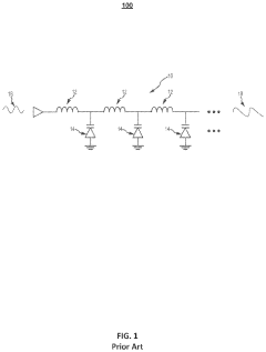
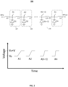
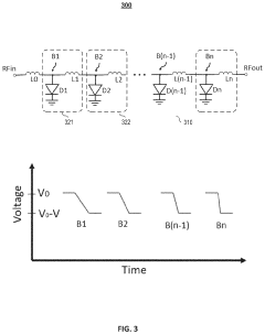
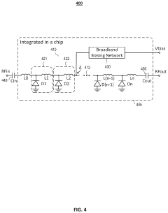
- The integration of a broadband biasing circuit and output DC blocking capacitor within a single chip, using a series of segments with non-linear shunt capacitors and series inductors, allows for improved impedance matching and generation of broadband harmonics, preventing RF signal leakage through the use of low-pass filters.
Mid-infrared optical frequency comb generation system and method based on manipulation of multi-photon absorption effect
PatentInactiveUS20210318591A1
Innovation
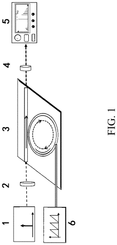
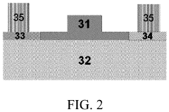
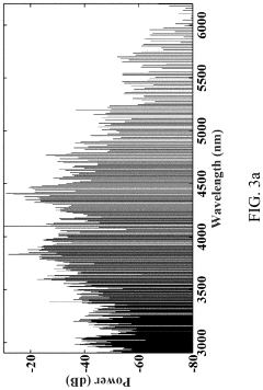
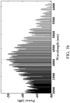
- A mid-infrared soliton-state OFC generation system based on the manipulation of the multi-photon absorption (MPA) effect, utilizing a pump light source unit, a microring resonator (MRR) unit, and an MPA effect control unit, where the MRR cavity is made of germanium to reduce linear loss and enhance nonlinear effects, and an arbitrary waveform generator is used to control free carrier density for generating ultra-broadband soliton-state OFCs.
Fabrication Techniques and Materials Science
The fabrication of integrated photonic devices for broadband microcomb generation requires sophisticated techniques and materials that can precisely control dispersion characteristics. Silicon nitride (Si₃N₄) has emerged as the leading material platform due to its wide transparency window (400-2500 nm), high refractive index (~2.0), and negligible nonlinear absorption in the telecommunications band. The CMOS compatibility of Si₃N₄ further enhances its appeal for large-scale manufacturing.
Advanced deposition techniques are critical for achieving the thick films (>700 nm) necessary for dispersion engineering. Low-pressure chemical vapor deposition (LPCVD) has become the standard approach, allowing for high-quality, low-loss Si₃N₄ films with precisely controlled stoichiometry. However, this process introduces significant film stress, which can cause cracking when depositing the thick layers required for anomalous dispersion in the near-infrared region.
Recent innovations have addressed this challenge through stress-release techniques such as crack barriers, thermal cycling, and photonic Damascene processes. The Damascene approach, pioneered by EPFL researchers, involves etching trenches in silicon dioxide, filling them with Si₃N₄, and then planarizing the surface. This method has enabled the fabrication of waveguides with heights exceeding 1.5 μm while maintaining propagation losses below 1 dB/m.
Alternative material platforms are also being explored, including aluminum nitride (AlN), tantala (Ta₂O₅), and lithium niobate on insulator (LNOI). Each offers unique advantages: AlN provides strong second-order nonlinearity, tantala offers higher refractive index contrast, and LNOI combines strong electro-optic effects with nonlinear properties. However, these materials generally present more complex fabrication challenges compared to Si₃N₄.
Precision lithography and etching processes are equally crucial for dispersion engineering. Electron-beam lithography enables nanometer-scale feature definition but faces throughput limitations for mass production. Deep-UV lithography offers a more scalable alternative while still achieving sub-100 nm resolution. The subsequent etching processes, typically using reactive ion etching (RIE) or inductively coupled plasma (ICP) etching, must maintain vertical sidewalls with minimal roughness to reduce scattering losses.
Surface roughness mitigation has become a key focus area, with techniques such as chemical-mechanical polishing (CMP) and thermal oxidation smoothing being employed to achieve ultra-low propagation losses. Recent demonstrations have achieved losses as low as 0.1 dB/m in Si₃N₄ waveguides, representing a critical advancement for high-Q resonators necessary for low-threshold comb generation.
Standardization Efforts in Integrated Photonics
Standardization efforts in the field of integrated photonics have become increasingly crucial for the advancement of technologies like integrated dispersion engineering for broadband microcomb generation. Several international organizations are actively working to establish common standards, protocols, and measurement techniques to ensure interoperability and reliability across different platforms and manufacturers.
The IEEE Photonics Society has established working groups specifically focused on standardizing key parameters for integrated photonic devices, including microresonators used in microcomb generation. These standards address critical aspects such as coupling efficiency metrics, quality factor measurement protocols, and dispersion characterization methodologies that are essential for reproducible microcomb generation.
Similarly, the International Electrotechnical Commission (IEC) has developed standards for integrated photonic circuits that encompass specifications for waveguide dimensions, material properties, and fabrication tolerances. These standards are particularly relevant for dispersion engineering, as they provide guidelines for achieving consistent dispersion profiles across different manufacturing runs and facilities.
The Photonic Integrated Circuit (PIC) Consortium has been instrumental in creating a standardized Process Design Kit (PDK) framework that includes dispersion engineering tools and models. This initiative enables designers to accurately predict and control dispersion characteristics in various material platforms, including silicon nitride, silicon, and lithium niobate—all critical materials for microcomb applications.
Regional standardization efforts are also noteworthy, with the European Telecommunications Standards Institute (ETSI) developing specifications for integrated photonic devices in telecommunications applications. Their work includes standardized testing procedures for group velocity dispersion measurement and anomalous dispersion verification, which directly impact broadband microcomb generation capabilities.
Industry consortia like AIM Photonics and PIXAPP have established foundry services with standardized design rules and process flows, creating multi-project wafer runs that adhere to consistent specifications. These initiatives have significantly lowered the barrier to entry for researchers and companies working on dispersion-engineered microcombs by providing access to reliable, standardized fabrication processes.
Despite these advances, challenges remain in standardizing novel dispersion engineering techniques, particularly those involving complex geometries or hybrid material systems. Ongoing efforts are focused on developing standards for emerging approaches such as subwavelength gratings, multi-layer waveguides, and heterogeneous integration methods that show promise for next-generation broadband microcomb technologies.
Unlock deeper insights with Patsnap Eureka Quick Research — get a full tech report to explore trends and direct your research. Try now!
Generate Your Research Report Instantly with AI Agent
Supercharge your innovation with Patsnap Eureka AI Agent Platform!
