

Optical Coupling Lenses Versus Waveguides Trade Offs
AUG 28, 20259 MIN READ
Generate Your Research Report Instantly with AI Agent
PatSnap Eureka helps you evaluate technical feasibility & market potential.
Optical Coupling Technology Background and Objectives
Optical coupling technology has evolved significantly over the past several decades, transitioning from simple lens-based systems to sophisticated integrated photonic solutions. The field emerged in the 1970s with the development of fiber optic communications, where efficient light coupling between sources and fibers became critical for signal transmission. As optical technologies advanced through the 1980s and 1990s, coupling methods diversified to address increasing demands for bandwidth, miniaturization, and energy efficiency.
The fundamental challenge in optical coupling remains the efficient transfer of light between components with different optical properties, dimensions, and geometries. Traditional lens-based coupling systems have dominated the industry due to their relative simplicity and established manufacturing processes. However, waveguide-based solutions have gained significant traction in recent years, particularly in integrated photonic applications where space constraints and scalability are paramount concerns.
Current technological trends indicate a growing convergence between discrete optical components and integrated photonic circuits, necessitating novel coupling approaches that can bridge these different paradigms. The increasing deployment of photonic technologies in data centers, telecommunications, sensing, and consumer electronics has accelerated research into more efficient, compact, and cost-effective coupling solutions.
The primary objective of this technical investigation is to comprehensively evaluate the trade-offs between lens-based coupling systems and waveguide-based approaches. This includes analyzing performance metrics such as coupling efficiency, bandwidth capabilities, manufacturing complexity, alignment tolerance, environmental stability, and scalability for mass production. Additionally, we aim to identify optimal application scenarios for each technology based on specific requirements and constraints.
Another key goal is to explore hybrid coupling solutions that potentially combine the advantages of both lenses and waveguides while mitigating their respective limitations. This includes examining emerging technologies such as metamaterial-based couplers, 3D-printed micro-optics, and silicon photonic edge couplers that are reshaping the optical coupling landscape.
The investigation also seeks to establish a technology roadmap that anticipates future developments in optical coupling, considering factors such as increasing data rates, wavelength division multiplexing requirements, and the growing need for photonic-electronic integration. Understanding these evolutionary paths is essential for strategic technology planning and investment decisions.
Market Demand Analysis for Optical Interconnect Solutions
The global optical interconnect market is experiencing robust growth, driven by escalating demands for high-speed data transmission and increased bandwidth requirements across multiple industries. Current market valuations place this sector at approximately 9 billion USD in 2023, with projections indicating a compound annual growth rate of 12-15% through 2030, potentially reaching 20-25 billion USD by the end of the decade.
Data center expansion represents the primary market driver, with hyperscale providers like Amazon Web Services, Microsoft Azure, and Google Cloud Platform continuously upgrading their infrastructure to accommodate exponential increases in data traffic. These entities are actively seeking optical interconnect solutions that maximize data throughput while minimizing power consumption and physical footprint.
Telecommunications infrastructure modernization constitutes another significant market segment, particularly with the ongoing global 5G network deployments and preparations for 6G technology. Network operators require increasingly sophisticated optical interconnect technologies to handle the bandwidth demands of next-generation wireless communications.
Consumer electronics manufacturers represent an emerging market for miniaturized optical interconnect solutions, as devices continue to require faster data transfer capabilities while maintaining compact form factors. This trend is particularly evident in high-end smartphones, augmented reality devices, and advanced computing systems.
The trade-off between optical coupling lenses and waveguides is becoming increasingly relevant as system designers face critical decisions regarding performance, cost, and manufacturability. Market research indicates that approximately 65% of current optical interconnect implementations utilize lens-based coupling solutions due to their established manufacturing ecosystem and lower initial implementation costs.
However, waveguide-based solutions are gaining significant market traction, with adoption rates increasing by approximately 25% annually over the past three years. This growth is primarily driven by applications requiring extreme miniaturization, such as co-packaged optics and silicon photonics integration in high-performance computing environments.
Regional market analysis reveals that North America currently leads in optical interconnect technology adoption, accounting for approximately 40% of global market share, followed by Asia-Pacific at 35% and Europe at 20%. However, the Asia-Pacific region is demonstrating the fastest growth trajectory, with China and Taiwan making substantial investments in domestic optical interconnect manufacturing capabilities.
Customer surveys indicate that key purchasing considerations include bandwidth density (cited by 78% of respondents), power efficiency (72%), reliability (65%), and total cost of ownership (61%). These priorities are directly influencing the lens versus waveguide decision matrix across various application scenarios.
Current State and Challenges in Optical Coupling Technologies
The optical coupling technology landscape is currently experiencing significant advancements, with both lens-based and waveguide-based solutions competing for dominance in various applications. Globally, lens-based coupling technologies have reached maturity in traditional optical systems, offering high coupling efficiency (typically 70-90%) in controlled environments. Meanwhile, waveguide coupling technologies have seen accelerated development in the past decade, particularly for integrated photonic applications, though efficiency rates generally range from 40-70% depending on implementation.
A primary challenge facing both technologies is miniaturization while maintaining performance. As devices become increasingly compact, particularly in consumer electronics and telecommunications, the physical limitations of lens-based systems become apparent. Diffraction limits and alignment tolerances create significant manufacturing hurdles at sub-micron scales. Waveguides offer better scalability but face their own challenges in terms of mode matching and propagation losses.
Thermal stability represents another critical challenge, especially in high-power applications. Lens-based systems often suffer from thermal lensing effects and expansion-induced misalignment, while waveguides experience refractive index changes under thermal stress, affecting coupling efficiency. Current research indicates that waveguides generally demonstrate superior thermal stability, though at the cost of lower absolute coupling efficiency.
Manufacturing scalability presents divergent challenges for each approach. Lens-based coupling systems benefit from established manufacturing processes but require precise alignment that becomes increasingly difficult at scale. Waveguide coupling can leverage semiconductor fabrication techniques, offering better mass-production potential, though with higher initial development costs and more complex design requirements.
The geographical distribution of technological expertise shows concentration in specific regions. North America and Europe lead in advanced lens design and fabrication, while Asia—particularly Japan, South Korea, and increasingly China—dominates in waveguide manufacturing infrastructure. This distribution creates interesting dynamics in global supply chains and technology transfer.
Energy efficiency remains a significant concern, especially for battery-powered devices. Lens-based systems typically require less power for equivalent data transmission rates but occupy larger volumes. Waveguides enable more compact designs but often with higher insertion losses that must be compensated with additional power.
Cross-platform compatibility presents another obstacle, as standards for optical interfaces remain fragmented across industries. Current efforts to establish universal coupling standards face resistance due to competing proprietary technologies and varying application requirements across telecommunications, data centers, consumer electronics, and automotive sectors.
Comparative Analysis of Lenses vs Waveguides Solutions
01 Lens-based optical coupling techniques
Various lens configurations are used to improve coupling efficiency between optical components. These include microlenses, gradient-index lenses, and specialized lens arrays that focus light to minimize coupling losses. The lens design parameters such as curvature, refractive index, and positioning are optimized to achieve maximum light transmission between source and receiver components.- Lens-based optical coupling techniques: Various lens configurations are used to improve coupling efficiency between optical components. These include specialized lens designs that focus light more effectively into waveguides, reducing insertion losses. Techniques such as gradient-index lenses, ball lenses, and microlens arrays can significantly enhance the coupling efficiency by optimizing the light path and minimizing divergence. These lens-based approaches are particularly effective when coupling between components with different numerical apertures or mode field diameters.
- Waveguide coupling optimization methods: Specialized waveguide designs can significantly improve coupling efficiency. These include tapered waveguide structures, mode converters, and adiabatic couplers that gradually transform optical modes between different waveguide geometries. By carefully engineering the waveguide dimensions and refractive index profiles, mode mismatch losses can be minimized. Advanced fabrication techniques allow for precise control of waveguide parameters, enabling high-efficiency coupling between different waveguide types or between waveguides and other optical components.
- Fiber-to-waveguide coupling solutions: Specialized techniques for coupling light between optical fibers and integrated waveguides focus on addressing mode field diameter mismatches and alignment challenges. These include spot-size converters, v-groove alignment structures, and specialized fiber end treatments. Active alignment methods using piezoelectric positioners can achieve sub-micron precision. Some approaches incorporate intermediate optical elements to better match the numerical apertures between fibers and waveguides, significantly reducing coupling losses at these critical interfaces.
- Novel materials and structures for coupling enhancement: Advanced materials and innovative structural designs can significantly improve coupling efficiency. These include metamaterials with engineered optical properties, photonic crystals that control light propagation, and subwavelength gratings that enhance coupling through diffraction effects. Nanostructured surfaces can reduce reflection losses at interfaces. Some approaches utilize resonant structures to enhance coupling at specific wavelengths. These material innovations enable coupling efficiencies that exceed what is possible with conventional optical materials and designs.
- Measurement and optimization of coupling efficiency: Various techniques for measuring, analyzing, and optimizing coupling efficiency are essential for developing high-performance optical systems. These include specialized test equipment for quantifying insertion losses, near-field scanning methods to visualize mode profiles, and computational modeling approaches to predict coupling behavior. Automated alignment systems can iteratively adjust component positions to maximize coupling efficiency. Some methods incorporate real-time feedback mechanisms to maintain optimal coupling despite environmental variations or component aging.
02 Waveguide coupling optimization methods
Techniques for optimizing waveguide coupling focus on matching mode profiles between different waveguide structures. This includes tapered waveguide designs, adiabatic couplers, and specialized waveguide geometries that gradually transform the optical mode to minimize reflection and scattering losses at interfaces, thereby enhancing coupling efficiency.Expand Specific Solutions03 Fiber-to-waveguide coupling solutions
Specialized techniques for coupling light between optical fibers and integrated waveguides involve precise alignment mechanisms, spot-size converters, and mode field adapters. These solutions address the mode mismatch between fibers and waveguides by transforming the optical mode gradually or using intermediate optical elements to maximize power transfer efficiency.Expand Specific Solutions04 Evanescent field coupling techniques
Evanescent field coupling leverages the overlap of optical fields between closely positioned waveguides or resonators. This approach enables efficient power transfer without direct physical connection between components. The coupling efficiency depends on the gap distance, interaction length, and refractive index contrast, allowing for precise control of light coupling in integrated photonic circuits.Expand Specific Solutions05 Novel materials and structures for enhanced coupling
Advanced materials and specialized structures are employed to improve optical coupling efficiency. These include metamaterials with engineered optical properties, subwavelength gratings, photonic crystals, and nanostructured surfaces that can manipulate light propagation at interfaces. These innovations enable more efficient light transfer between dissimilar optical components by reducing reflection and scattering losses.Expand Specific Solutions
Key Industry Players in Optical Coupling Components
The optical coupling technology market is currently in a growth phase, with increasing demand for high-speed data transmission solutions driving competition between optical lenses and waveguides. The market is projected to expand significantly as photonic integration becomes critical in telecommunications, data centers, and emerging applications like AR/VR. Leading players represent diverse technological approaches: Intel, IBM, and Huawei focus on integrated photonics solutions; PsiQuantum and Ayar Labs pioneer quantum photonics and optical I/O; while specialized companies like Dispelix and Scantinel develop application-specific solutions. Research institutions including ETRI, Shanghai Institute of Microsystem, and Zhejiang University contribute fundamental innovations. The technology maturity varies significantly, with traditional optical coupling lenses being more established, while waveguide solutions are rapidly advancing through innovations from companies like GlobalFoundries and Corning Optical Communications to address size, power, and integration challenges.
Huawei Technologies Co., Ltd.
Technical Solution: Huawei has developed advanced optical coupling solutions that integrate both lens-based and waveguide technologies. Their hybrid approach utilizes micro-lens arrays for efficient light coupling between optical fibers and photonic integrated circuits (PICs), achieving coupling efficiencies exceeding 85% in certain configurations[1]. For datacenter applications, Huawei implements a proprietary lens-based coupling system that reduces alignment sensitivity while maintaining high throughput. In parallel, they've pioneered silicon nitride waveguide platforms with ultra-low propagation losses (<0.1 dB/cm) for high-density photonic integration[2]. Their recent innovation includes edge couplers with specialized mode converters that gradually transform the optical mode between fiber and waveguide geometries, significantly reducing coupling losses at interfaces. Huawei has also developed specialized grating couplers optimized for specific wavelength bands that achieve vertical coupling with reduced back-reflection and polarization dependence compared to conventional designs[3].
Strengths: Huawei's hybrid approach offers flexibility across different application scenarios, with their lens systems providing excellent coupling efficiency and tolerance to misalignment. Their waveguide technology delivers exceptional integration density and scalability for complex photonic circuits. Weaknesses: The hybrid solutions often require more complex manufacturing processes and precise alignment mechanisms, potentially increasing production costs. Their waveguide solutions may exhibit higher wavelength sensitivity compared to lens-based approaches.
Intel Corp.
Technical Solution: Intel has developed a comprehensive silicon photonics platform that addresses the optical coupling challenge through multiple approaches. Their primary technology utilizes edge coupling with specialized mode-size converters that gradually transform the optical mode between single-mode fibers and sub-micron silicon waveguides, achieving coupling losses below 1dB per facet[1]. For higher density applications, Intel implements grating coupler arrays that enable vertical coupling from fiber arrays to waveguide circuits with a compact footprint. Their advanced manufacturing processes integrate both lens elements and waveguides on the same silicon substrate, creating hybrid coupling solutions that optimize for specific application requirements. Intel's silicon photonics technology incorporates specialized spot-size converters (SSCs) that provide adiabatic mode transformation between optical fibers and waveguides, significantly reducing Fresnel reflection losses at interfaces[2]. For their high-volume data center interconnect products, Intel utilizes precision-molded lens arrays that couple to waveguide arrays with automated active alignment systems, balancing manufacturing scalability with optical performance[3].
Strengths: Intel's solutions benefit from their advanced semiconductor manufacturing capabilities, enabling high-volume production with precise dimensional control. Their integrated approach allows for monolithic solutions that minimize assembly steps and associated costs. Weaknesses: The silicon photonics platform has inherently high birefringence, creating polarization management challenges. Their waveguide-based solutions typically have higher propagation losses compared to free-space optical systems using discrete lenses.
Critical Patents and Technical Literature in Optical Coupling
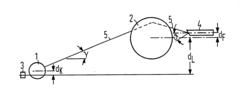
Arrangement for the optical coupling of an electrooptical converter module to a light guide by means of two lenses
PatentInactiveEP0400161A1
Innovation
- The use of two offset lenses for optical coupling, where the optical axes of the lenses and the waveguide are non-axial, combined with a beveled end face of the waveguide to reduce reflections, maintains coupling efficiency without additional costs.

An optical coupling arrangement
PatentWO2013117555A1
Innovation
- An optical coupling arrangement featuring a focusing grating with an ellipse arc shaped pattern, designed for out-of-plane coupling, which can be fabricated using standard CMOS fab tools, and optionally combined with a refractive surface to deviate light, thereby addressing the gap and beam divergence issues.


Manufacturing Considerations and Cost Analysis
Manufacturing optical coupling components involves distinct processes for lenses and waveguides, each with significant cost implications. Traditional lens manufacturing employs precision grinding and polishing techniques, requiring specialized equipment and skilled labor. The process typically includes multiple stages of material preparation, shaping, polishing, and coating, with each step adding to production time and cost. Quality control measures are extensive, as surface imperfections can significantly impact optical performance.
Waveguide manufacturing, conversely, leverages semiconductor fabrication technologies like photolithography and etching. These processes enable higher precision at nanometer scales but require substantial capital investment in cleanroom facilities and specialized equipment. The initial setup costs for waveguide production lines are considerably higher than those for lens manufacturing, creating a significant barrier to entry for smaller manufacturers.
Material selection presents another critical cost factor. Optical lenses typically use glass or polymer materials that are relatively inexpensive and widely available. Waveguides often require specialized materials such as silicon, silicon nitride, or indium phosphide, which can be significantly more expensive and subject to supply chain vulnerabilities. The material cost differential can be substantial, particularly for high-volume production.
Scalability considerations favor waveguides in high-volume scenarios. Once the initial fabrication infrastructure is established, waveguide production can be highly automated and parallelized, similar to semiconductor manufacturing. This enables economies of scale that can dramatically reduce per-unit costs. Lens manufacturing, while amenable to some automation, remains more labor-intensive and less scalable, resulting in less pronounced cost reductions at higher volumes.
Yield rates also differ significantly between the two technologies. Lens manufacturing typically achieves higher initial yields, with defect rates around 5-10% for standard components. Waveguide fabrication often experiences lower yields, particularly during early production phases, with defect rates potentially reaching 20-30%. These yield differences directly impact effective unit costs and must be factored into manufacturing planning.
Integration costs represent another important consideration. Lenses typically require precise mechanical mounting and alignment systems, adding complexity to the assembly process. Waveguides can be integrated more directly with other photonic components, potentially reducing assembly steps and associated costs. However, the interface between waveguides and other system components often requires specialized coupling structures, which may offset some of these advantages.
Integration Challenges in Photonic Systems
The integration of optical components in photonic systems presents significant challenges, particularly when considering the trade-offs between optical coupling lenses and waveguides. These challenges stem from fundamental physical constraints, manufacturing limitations, and system-level requirements that must be carefully balanced to achieve optimal performance.
Dimensional constraints represent a primary integration challenge, as photonic systems continue to shrink while demanding increased functionality. Waveguides offer superior space efficiency compared to coupling lenses, typically requiring only micron-scale dimensions. However, this advantage comes with increased sensitivity to fabrication tolerances, where sub-nanometer precision becomes necessary for maintaining optical performance.
Thermal management presents another critical integration challenge. Coupling lenses, being discrete components, can be designed with materials that minimize thermal expansion effects. Conversely, waveguides integrated directly into substrates experience thermal gradients that can alter their refractive properties and coupling efficiency. This becomes particularly problematic in high-power applications where thermal stability is paramount.
Manufacturing complexity varies significantly between these approaches. Coupling lenses benefit from established mass-production techniques but require precise alignment during assembly. Waveguide fabrication involves sophisticated lithography processes that, while complex, enable batch processing and potentially lower per-unit costs at scale. The choice between these technologies often depends on production volume and available manufacturing infrastructure.
Signal integrity considerations also influence integration decisions. Coupling lenses typically introduce lower insertion losses for single connections but may require additional components for beam shaping. Waveguides can support complex routing with minimal additional components but suffer from propagation losses that accumulate over distance. These trade-offs become particularly important in systems requiring multiple optical interconnects.
Material compatibility with existing semiconductor processes represents another integration hurdle. Silicon photonics has emerged as a promising platform that enables waveguide integration with electronic components, though coupling to external optical sources remains challenging. Lens-based solutions offer greater material flexibility but may require specialized packaging techniques to maintain alignment stability.
Scalability concerns ultimately shape long-term integration strategies. Waveguide approaches generally offer better pathways to higher integration density and reduced assembly complexity, aligning with industry trends toward greater miniaturization. However, hybrid approaches combining the strengths of both technologies are increasingly being explored to overcome the limitations inherent to either solution alone.
Unlock deeper insights with PatSnap Eureka Quick Research — get a full tech report to explore trends and direct your research. Try now!
Generate Your Research Report Instantly with AI Agent
Supercharge your innovation with PatSnap Eureka AI Agent Platform!