

SNSPD Fabrication Process Control For Uniformity Across Chips
AUG 28, 202510 MIN READ
Generate Your Research Report Instantly with AI Agent
PatSnap Eureka helps you evaluate technical feasibility & market potential.
SNSPD Technology Evolution and Fabrication Goals
Superconducting Nanowire Single Photon Detectors (SNSPDs) have undergone remarkable evolution since their initial demonstration in the early 2000s. The technology originated from basic superconducting thin film research, evolving through several critical phases to become one of the most promising single-photon detection technologies available today. Early SNSPDs suffered from limited detection efficiency and significant non-uniformity issues, with performance varying dramatically across fabricated devices.
The technological progression of SNSPDs has been characterized by continuous improvements in material science, nanofabrication techniques, and cryogenic integration methods. Initial devices utilized simple straight nanowire geometries fabricated from niobium nitride (NbN) films, while modern designs incorporate complex meandering patterns, optical cavities, and advanced superconducting materials such as tungsten silicide (WSi) and molybdenum silicide (MoSi) to enhance performance metrics.
A pivotal advancement came with the transition from electron-beam lithography to more sophisticated nanofabrication techniques, enabling precise control over nanowire dimensions at the sub-10nm scale. This evolution has been crucial for addressing the fundamental challenge of fabrication uniformity, which directly impacts device yield and performance consistency across chips.
The current technological frontier focuses on achieving unprecedented uniformity in critical device parameters including nanowire width, film thickness, and superconducting properties across entire wafers. This represents a significant shift from earlier research paradigms that prioritized performance optimization of individual devices toward manufacturing scalability and reproducibility.
Key fabrication goals for next-generation SNSPDs include achieving less than 5% variation in critical current across all devices on a single chip, maintaining nanowire width uniformity within ±1nm tolerance, and ensuring homogeneous superconducting transition temperatures with variations below 0.1K. These stringent requirements are driven by emerging applications in quantum information processing, where system-level performance depends critically on the uniformity of component detectors.
The technology roadmap also emphasizes the development of non-destructive testing methodologies that can be integrated into the fabrication workflow, enabling real-time process control and adaptive manufacturing techniques. This includes advanced metrology systems for in-situ monitoring of film deposition parameters and post-processing characterization tools that can identify non-uniformities before final device packaging.
Ultimately, the evolution of SNSPD fabrication technology is converging toward industrial-scale production capabilities that can deliver consistent, high-performance devices with predictable characteristics. This transition from laboratory curiosity to engineered system component represents both the greatest challenge and opportunity in the field, with significant implications for quantum technologies, astronomical instrumentation, and advanced sensing applications.
Market Analysis for High-Uniformity SNSPD Applications
The global market for Superconducting Nanowire Single-Photon Detectors (SNSPDs) with high uniformity across chips is experiencing significant growth, driven by increasing demands in quantum computing, quantum communication, and advanced scientific research applications. The current market size for high-performance photon detection systems is estimated at $450 million, with SNSPDs representing a rapidly expanding segment projected to grow at a compound annual rate of 23% through 2028.
Quantum information processing represents the largest application segment, accounting for approximately 42% of the SNSPD market. The critical requirement for highly uniform detection efficiency across large arrays is particularly pronounced in quantum computing applications, where error rates directly impact computational fidelity. Commercial quantum computing companies are increasingly investing in high-uniformity SNSPD technology as a key enabling component for scalable quantum systems.
Quantum communication networks, particularly quantum key distribution (QKD) systems, constitute the second-largest market segment at 28%. These applications demand consistent detection performance across multiple channels to maintain secure communication protocols. The deployment of satellite-based quantum communication systems by several nations has further accelerated demand for highly uniform SNSPDs capable of operating in space environments.
Scientific research applications, including advanced spectroscopy, LIDAR systems, and deep-space optical communication, represent 18% of the current market. These specialized applications often require customized SNSPD arrays with specific uniformity parameters, creating premium-priced market opportunities for manufacturers capable of delivering consistent performance metrics.
Geographically, North America leads the market with 39% share, followed by Asia-Pacific (33%) and Europe (24%). China has emerged as the fastest-growing regional market, with government investments in quantum technologies exceeding $15 billion over the next five years. Japan and South Korea are similarly expanding their quantum infrastructure, creating substantial demand for high-uniformity SNSPDs.
Industry analysis indicates that customers are willing to pay premium prices (30-50% above standard detectors) for SNSPDs demonstrating less than 5% variation in critical parameters across chips. This price sensitivity reflects the downstream costs associated with non-uniform detection in complex quantum systems, where recalibration and error correction impose significant operational overhead.
Market forecasts suggest that achieving consistent fabrication processes for uniform SNSPDs could unlock an additional $180 million in market value by 2026, primarily by enabling larger detector arrays suitable for more complex quantum applications currently constrained by uniformity limitations.
Current Fabrication Challenges and Uniformity Limitations
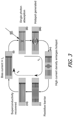
Superconducting Nanowire Single-Photon Detectors (SNSPDs) fabrication faces significant challenges in achieving uniform performance across chips. The primary limitation stems from the extreme sensitivity of these devices to nanoscale variations in geometry. Even minor fluctuations in nanowire width (on the order of 1-2 nm) can dramatically alter critical current density and detection efficiency, resulting in inconsistent performance between devices on the same chip.
Lithography precision represents a fundamental challenge, particularly when fabricating nanowires with widths below 100 nm. Electron beam lithography, while offering high resolution, suffers from proximity effects and beam stability issues that introduce variations across large-area exposures. These variations become more pronounced when scaling to wafer-level production, where beam drift and focus inconsistencies create non-uniform feature sizes.
Film deposition uniformity presents another critical challenge. The superconducting thin films (typically NbN, NbTiN, or WSi) must maintain consistent thickness and composition across the entire substrate. Current sputtering and atomic layer deposition techniques struggle to achieve thickness variations below ±2% across a 4-inch wafer, which directly impacts the superconducting properties of the nanowires.
Etching processes further compound uniformity issues. Reactive ion etching and other plasma-based techniques exhibit loading effects and chamber conditions that vary spatially, resulting in different etch rates and profiles across the substrate. This leads to inconsistent nanowire widths and sidewall quality, which directly affects detector performance.
Environmental control during fabrication represents an often-overlooked challenge. Temperature fluctuations, humidity variations, and airborne particulates can all impact critical process steps. Even minor contamination can create localized defects that serve as weak points in the nanowires, leading to premature switching or reduced critical currents.
Substrate quality and preparation significantly influence device uniformity. Surface roughness, crystal defects, and chemical residues can affect film adhesion and growth characteristics. These substrate-related variations often manifest as inconsistent superconducting properties across the chip, even when other process parameters remain constant.
Metrology limitations further complicate process control efforts. Current inspection techniques struggle to provide accurate, high-throughput measurements of nanowire dimensions and film properties across entire chips. This makes it difficult to implement effective feedback loops for process optimization and quality control.
The cumulative effect of these challenges results in yield issues that severely limit commercial viability. Typical SNSPD fabrication processes achieve only 30-60% yield of devices meeting performance specifications on a single chip, with significant variations in detection efficiency, dark count rate, and timing jitter between devices. This inconsistency necessitates extensive post-fabrication testing and selection, substantially increasing production costs and limiting scalability.
State-of-the-Art Process Control Methodologies
01 Fabrication techniques for uniform SNSPDs
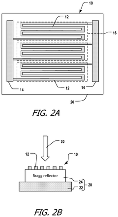
Various fabrication techniques are employed to enhance the uniformity of Superconducting Nanowire Single Photon Detectors (SNSPDs). These include precise deposition methods for superconducting films, advanced lithography processes to ensure consistent nanowire dimensions, and controlled etching procedures. These techniques help minimize variations in critical current density and thickness across the detector, resulting in more uniform detection efficiency and reduced timing jitter.- Fabrication methods for uniform SNSPDs: Various fabrication techniques are employed to enhance the uniformity of Superconducting Nanowire Single Photon Detectors. These include precise deposition methods for superconducting films, controlled etching processes, and advanced lithography techniques that ensure consistent nanowire dimensions across the detector area. Uniform fabrication reduces variations in critical current and detection efficiency, leading to more reliable SNSPD performance.
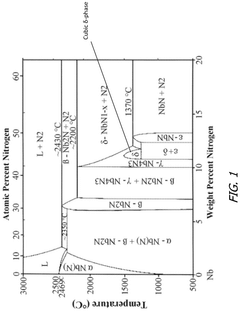
- Material selection and composition for uniform SNSPDs: The choice of superconducting materials and their composition significantly impacts SNSPD uniformity. Researchers have explored various superconducting materials including niobium nitride (NbN), niobium titanium nitride (NbTiN), and amorphous materials that offer improved homogeneity. Careful control of film stoichiometry, thickness, and crystalline structure helps achieve uniform superconducting properties across the nanowire, resulting in consistent photon detection performance.
- Design optimization for SNSPD uniformity: Innovative design approaches are implemented to enhance SNSPD uniformity. These include optimized meandering patterns, variable nanowire widths, and novel geometric configurations that distribute current density more evenly. Some designs incorporate parallel nanowire structures or segmented designs to mitigate the impact of local defects. Advanced modeling and simulation techniques help predict and optimize detector uniformity before fabrication.
- Testing and characterization methods for SNSPD uniformity: Specialized testing and characterization techniques are developed to assess and verify SNSPD uniformity. These include spatially-resolved detection efficiency mapping, critical current distribution measurements, and advanced imaging techniques that can identify nanoscale variations. Real-time monitoring during operation helps identify non-uniform regions, while statistical analysis methods quantify uniformity across large detector arrays.
- Post-fabrication treatments to improve SNSPD uniformity: Various post-fabrication treatments are employed to enhance SNSPD uniformity after initial production. These include thermal annealing processes, surface passivation techniques, and controlled aging procedures that stabilize superconducting properties. Some approaches utilize targeted laser or ion beam treatments to adjust local properties of the nanowires, while others implement protective coatings to prevent environmental degradation that could lead to non-uniformities over time.
02 Material selection and optimization for SNSPD uniformity
The choice and optimization of superconducting materials significantly impact SNSPD uniformity. Materials such as NbN, NbTiN, WSi, and MoSi are carefully selected and processed to achieve consistent superconducting properties. Techniques like alloying, doping, and precise control of stoichiometry help achieve uniform superconducting gap energy and critical temperature across the nanowire, enhancing detection uniformity and reducing dark count rates.Expand Specific Solutions03 Design optimization for spatial uniformity
Innovative design approaches are implemented to improve the spatial uniformity of SNSPDs. These include meandering patterns with consistent bend radii, parallel nanowire configurations, and optimized fill factors. Advanced designs incorporate gradient-thickness structures and variable-width nanowires to compensate for current crowding effects at bends. These design optimizations ensure uniform photon detection efficiency across the entire active area of the detector.Expand Specific Solutions04 Testing and characterization methods for uniformity assessment
Specialized testing and characterization techniques are developed to assess and verify SNSPD uniformity. These include spatially-resolved detection efficiency mapping, critical current distribution analysis, and timing jitter measurements across different detector regions. Advanced imaging techniques such as scanning electron microscopy and atomic force microscopy are employed to correlate physical characteristics with detection performance, enabling targeted improvements in uniformity.Expand Specific Solutions05 Post-fabrication treatments to enhance uniformity
Various post-fabrication treatments are applied to improve SNSPD uniformity. These include thermal annealing processes to homogenize material properties, passivation layers to protect against environmental degradation, and controlled aging procedures to stabilize performance. Techniques such as ion irradiation and laser trimming are also employed to fine-tune local properties of the nanowires, resulting in more uniform detection characteristics across the entire device.Expand Specific Solutions
Leading Research Groups and Commercial SNSPD Manufacturers
The SNSPD fabrication process control market is currently in a growth phase, with increasing demand for uniform superconducting nanowire single-photon detectors across various quantum applications. The market size is expanding as quantum technologies gain commercial traction, estimated to reach several hundred million dollars by 2025. Technologically, the field shows moderate maturity with significant room for advancement. Leading semiconductor manufacturers like TSMC, Samsung Electronics, and GlobalFoundries possess advanced fabrication capabilities applicable to SNSPD production, while specialized equipment providers including Tokyo Electron, Lam Research, and Applied Materials offer critical process control solutions. Companies like IBM and Infineon Technologies are driving innovation in superconducting device fabrication, focusing on improving yield and uniformity across chips - a key challenge that remains for widespread commercial adoption of SNSPD technology.
Taiwan Semiconductor Manufacturing Co., Ltd.
Technical Solution: TSMC has developed a sophisticated SNSPD fabrication process control system focused on achieving nanometer-scale uniformity across chips. Their approach leverages advanced 300mm wafer processing techniques adapted specifically for superconducting materials. TSMC's process begins with ultra-clean substrate preparation using proprietary surface conditioning methods that reduce defect density to less than 0.1 defects/cm². For superconducting film deposition, they employ modified physical vapor deposition (PVD) systems with rotating substrate holders and multiple sensors that ensure thickness uniformity within ±1% across entire wafers. Their nanowire patterning utilizes advanced immersion lithography combined with specialized etching processes that maintain critical dimension control within 1nm across the chip. TSMC has implemented an integrated metrology system that performs measurements at over 20 points across each wafer after critical process steps, feeding data into a statistical process control system that automatically adjusts process parameters to maintain uniformity. Additionally, they've developed non-destructive testing methods that can evaluate superconducting properties at room temperature, allowing for 100% inspection before cryogenic testing.
Strengths: TSMC's world-leading semiconductor fabrication expertise provides unparalleled process control capabilities and quality management systems. Their extensive experience with high-volume manufacturing enables consistent results across large production runs. Weaknesses: Their processes may be optimized for traditional CMOS fabrication rather than the specific requirements of superconducting materials, potentially requiring significant adaptation for optimal SNSPD performance.
Lam Research Corp.
Technical Solution: Lam Research has developed specialized SNSPD fabrication process control solutions focused on achieving uniformity across chips. Their approach centers on advanced thin film deposition and etching technologies specifically optimized for superconducting materials. Lam's VECTOR® platform has been adapted for superconducting thin film deposition with enhanced temperature control systems that maintain substrate temperatures within ±0.3°C across 300mm wafers, critical for uniform nucleation and growth of materials like NbN and WSi. Their process incorporates real-time monitoring using spectroscopic ellipsometry that provides feedback on film thickness and composition during deposition, enabling dynamic adjustments to maintain uniformity. For nanowire patterning, Lam has developed specialized plasma etching processes with advanced endpoint detection that prevents over-etching while ensuring complete pattern transfer. Their Sense.i® platform includes proprietary algorithms that analyze process data across multiple wafers to identify drift patterns before they impact device performance. Lam's approach also includes specialized cleaning processes designed to remove contaminants without damaging sensitive superconducting films, a critical factor in maintaining uniform performance across devices.
Strengths: Lam Research's deep expertise in etch and deposition technologies provides highly specialized solutions for the most critical steps in SNSPD fabrication. Their equipment includes advanced process control systems that can be specifically tuned for superconducting materials. Weaknesses: As primarily an equipment provider rather than a device manufacturer, their solutions require integration with other process steps and may not address all aspects of SNSPD fabrication uniformity challenges.
Critical Patents in SNSPD Fabrication Uniformity
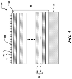
SNSPD with integrated aluminum nitride seed or waveguide layer
PatentActiveUS12317758B2
Innovation
- The implementation of a seed layer of metal nitride, such as aluminum nitride, below the superconductive wire in the SNSPD device, which improves the critical temperature of the niobium nitride layer and enhances the material quality and light absorption efficiency.
Method and systems for fabricating superconducting nanowire single photon detector (SNSPD)
PatentPendingUS20230031577A1
Innovation
- A method and system for fabricating superconducting nanowire single photon detectors using high temperature superconductors with pulsed laser deposition, eliminating post-processing of superconducting thin films and gold encapsulation to maintain material quality and enable operation above 4 K.
Material Science Innovations for SNSPD Performance
Material science innovations have been pivotal in advancing Superconducting Nanowire Single Photon Detector (SNSPD) performance. The traditional NbN-based SNSPDs have been complemented by alternative materials such as WSi, MoSi, and NbTiN, each offering unique advantages for specific applications. These material innovations have directly addressed critical performance parameters including detection efficiency, dark count rates, and timing resolution.
Recent breakthroughs in amorphous superconducting materials have demonstrated superior uniformity across larger areas compared to their crystalline counterparts. WSi, in particular, has shown exceptional promise with its lower energy gap and higher kinetic inductance, enabling higher detection efficiencies at longer wavelengths. However, these amorphous materials typically operate at sub-1K temperatures, presenting significant cryogenic challenges for practical deployment.
Multilayer heterostructures represent another frontier in SNSPD material science. By engineering superconducting-normal metal interfaces, researchers have achieved enhanced control over superconducting properties. These structures facilitate precise manipulation of the superconducting order parameter, critical for optimizing detector performance while maintaining fabrication uniformity across chips.
Surface passivation techniques have emerged as crucial for maintaining SNSPD performance stability. Thin oxide or nitride layers applied post-fabrication protect the superconducting nanowires from environmental degradation while minimizing impact on optical absorption and superconducting properties. Advanced passivation methods using atomic layer deposition have shown particular promise for creating uniform protective barriers.
Substrate engineering has also proven essential for SNSPD performance optimization. Materials such as sapphire, silicon, and silicon dioxide offer varying degrees of thermal conductivity and optical properties. Recent innovations include suspended nanowire structures that minimize substrate-induced thermal effects and enhance reset times through improved heat dissipation pathways.
The integration of optical cavity structures with carefully selected superconducting materials has led to significant enhancements in absorption efficiency. These structures, when precisely engineered, can achieve near-unity absorption at target wavelengths while maintaining the critical superconducting properties necessary for detection. This approach has proven particularly valuable for achieving uniformity in spectral response across multiple devices on a single chip.
Strain engineering represents a promising direction for further material innovation. By controlling the strain state of superconducting thin films through substrate lattice matching or post-deposition treatments, researchers can fine-tune critical current densities and transition temperatures across entire wafers, addressing one of the fundamental challenges in achieving chip-scale uniformity in SNSPD fabrication.
Metrology Techniques for Nanoscale Quality Assurance
Metrology techniques play a crucial role in ensuring the uniformity and quality of Superconducting Nanowire Single Photon Detectors (SNSPDs) during fabrication. Advanced measurement tools and methodologies are essential for characterizing nanoscale features that directly impact device performance and yield rates across chips.
Atomic Force Microscopy (AFM) represents one of the primary metrology techniques for SNSPD fabrication, offering sub-nanometer resolution for surface topology analysis. This capability allows manufacturers to verify nanowire width consistency and detect potential defects that could lead to non-uniform superconducting properties. AFM measurements can be performed at multiple stages of the fabrication process to track dimensional changes and ensure adherence to design specifications.
Scanning Electron Microscopy (SEM) provides complementary capabilities by enabling high-resolution imaging of nanowire patterns and edge definition. The non-contact nature of SEM makes it particularly valuable for inspecting delicate SNSPD structures without risking damage. Modern SEM systems equipped with automated pattern recognition can rapidly scan entire wafers to identify deviations in critical dimensions across multiple chips.
Spectroscopic ellipsometry has emerged as an essential technique for monitoring film thickness uniformity, a parameter directly linked to SNSPD detection efficiency. This optical method allows for non-destructive measurement of ultrathin superconducting films with precision in the sub-nanometer range. Mapping thickness variations across wafers helps identify process inconsistencies that may affect device-to-device uniformity.
X-ray Photoelectron Spectroscopy (XPS) and Auger Electron Spectroscopy (AES) provide critical information about material composition and potential contamination at interfaces. These techniques can detect subtle variations in stoichiometry or the presence of oxidation that might compromise superconducting properties. Depth profiling capabilities allow for analysis of multilayer structures common in advanced SNSPD designs.
Electrical testing methodologies complement physical metrology by directly measuring superconducting properties. Four-point probe measurements of sheet resistance at room temperature serve as early indicators of film quality, while low-temperature characterization provides critical information about transition temperature uniformity across chips. Resistance mapping techniques can identify potential "hot spots" where device performance might deviate from specifications.
Real-time monitoring systems are increasingly being integrated into SNSPD fabrication lines, allowing for in-situ measurement during critical process steps. These systems enable immediate feedback for process adjustment, reducing the likelihood of producing non-uniform devices. Machine learning algorithms are being developed to analyze metrology data streams and predict potential uniformity issues before they manifest in completed devices.
Unlock deeper insights with PatSnap Eureka Quick Research — get a full tech report to explore trends and direct your research. Try now!
Generate Your Research Report Instantly with AI Agent
Supercharge your innovation with PatSnap Eureka AI Agent Platform!