

SNSPD Integration On Photonic Integrated Circuits Techniques
AUG 28, 202510 MIN READ
Generate Your Research Report Instantly with AI Agent
PatSnap Eureka helps you evaluate technical feasibility & market potential.
SNSPD-PIC Integration Background and Objectives
Superconducting Nanowire Single-Photon Detectors (SNSPDs) have emerged as a revolutionary technology in quantum photonics, offering unprecedented detection efficiency, low dark count rates, and picosecond timing resolution. The integration of SNSPDs with Photonic Integrated Circuits (PICs) represents a critical frontier in quantum information processing, quantum communication, and quantum computing applications. This technological convergence aims to overcome the limitations of traditional bulk optical systems by enabling scalable, miniaturized quantum photonic platforms.
The evolution of SNSPD technology began in the early 2000s with the demonstration of superconducting nanowires as efficient single-photon detectors. Initially developed as standalone devices requiring complex cryogenic setups, SNSPDs have progressively evolved toward integration with waveguide structures. Concurrently, photonic integrated circuit technology has advanced significantly, with platforms based on silicon, silicon nitride, and III-V semiconductors achieving remarkable capabilities in manipulating light at the chip scale.
The integration of these two technologies addresses several critical challenges in quantum photonics. Traditional approaches involving fiber-coupled SNSPDs suffer from coupling losses, alignment complexities, and fundamental limitations in scalability. By directly integrating SNSPDs onto photonic chips, researchers aim to achieve near-unity detection efficiency, minimal optical losses, and the ability to scale to complex multi-detector configurations necessary for advanced quantum applications.
Current technical objectives for SNSPD-PIC integration focus on several key areas: achieving high coupling efficiency between waveguides and nanowires, maintaining detector performance metrics (efficiency, timing resolution, dark count rate) in the integrated environment, developing fabrication processes compatible with both superconducting materials and photonic structures, and ensuring reliable operation within cryogenic environments.
The field is witnessing a convergence of multiple disciplines, including superconducting physics, nanofabrication, integrated photonics, and quantum information science. This interdisciplinary nature has accelerated innovation but also introduced complex technical challenges requiring coordinated research efforts across traditionally separate domains.
Looking forward, the technology roadmap for SNSPD-PIC integration aims toward fully integrated quantum photonic systems incorporating multiple components—sources, detectors, and processing elements—on a single chip. This vision aligns with broader quantum technology initiatives worldwide, which recognize integrated quantum photonics as a promising platform for practical quantum information processing systems.
The ultimate goal extends beyond mere component integration to realizing complete quantum photonic systems capable of addressing applications in secure communication, quantum simulation, and eventually fault-tolerant quantum computing, positioning SNSPD-PIC integration as a foundational technology for the emerging quantum industry.
Market Analysis for Integrated Quantum Photonic Devices
The global market for integrated quantum photonic devices is experiencing unprecedented growth, driven by advancements in quantum computing, secure communications, and sensing applications. The integration of Superconducting Nanowire Single-Photon Detectors (SNSPDs) on Photonic Integrated Circuits (PICs) represents a critical enabling technology for this emerging market. Current market valuations place the quantum photonics sector at approximately $650 million in 2023, with projections indicating a compound annual growth rate of 29.8% through 2030.
The demand for integrated quantum photonic solutions is primarily fueled by government initiatives in quantum technologies, with the United States, China, and European Union collectively allocating over $30 billion in funding over the next decade. This substantial investment reflects the strategic importance of quantum technologies for national security and economic competitiveness.
Commercial demand is emerging across multiple sectors. Financial institutions are exploring quantum-secured communications for transaction security, while pharmaceutical companies are investigating quantum computing applications for drug discovery processes. The telecommunications industry represents another significant market segment, with major providers investing in quantum key distribution networks that rely heavily on integrated single-photon detection capabilities.
Market segmentation reveals distinct application categories for SNSPD-integrated photonic circuits. Quantum computing applications currently represent 42% of market demand, followed by quantum communications at 38%, and quantum sensing at 20%. This distribution is expected to shift as quantum sensing applications mature, potentially capturing up to 35% of the market by 2028.
Regional analysis shows North America leading with 41% market share, followed by Asia-Pacific at 32%, Europe at 24%, and other regions at 3%. China's aggressive investments in quantum technologies are rapidly closing the gap with Western markets, with domestic companies like Origin Quantum and SpinQ Technologies gaining significant traction.
The customer landscape is currently dominated by research institutions and government agencies, accounting for 73% of current purchases. However, enterprise adoption is accelerating, with private sector procurement expected to reach 45% of the market by 2027. This transition from research to commercial applications represents a critical inflection point for market growth.
Supply chain considerations reveal potential bottlenecks in specialized materials and fabrication capabilities. The limited number of facilities capable of producing high-quality superconducting nanowires integrated with photonic circuits represents a significant constraint on market expansion. Companies that can successfully address these manufacturing challenges stand to capture substantial market share.
SNSPD-PIC Integration Challenges and Global Development Status
The integration of Superconducting Nanowire Single-Photon Detectors (SNSPDs) with Photonic Integrated Circuits (PICs) represents a significant technological frontier in quantum photonics. Globally, this integration faces substantial challenges that have shaped development trajectories across different regions. These challenges primarily stem from the fundamental incompatibility between the cryogenic operating requirements of SNSPDs (typically below 4K) and the room-temperature design of most photonic platforms.
Material compatibility presents a critical hurdle, as superconducting materials like NbN, NbTiN, or WSi must maintain their properties when deposited on photonic substrates such as silicon, silicon nitride, or lithium niobate. The thermal expansion coefficient mismatch between these materials often leads to film stress and potential delamination during thermal cycling, compromising device performance and reliability.
Fabrication process integration remains exceptionally challenging, requiring precise nanofabrication techniques to create nanowires with widths of 50-100nm while preserving the optical properties of the underlying waveguides. The sequential processing steps must be carefully orchestrated to prevent cross-contamination or damage to previously fabricated structures.
Coupling efficiency between waveguides and nanowires represents another significant technical barrier. Achieving high optical absorption in the nanowire while maintaining low insertion loss in the photonic circuit demands sophisticated optical design and precise alignment during fabrication, with tolerances often in the nanometer range.
The development status varies significantly across different regions. North America, particularly the United States, leads in fundamental research through institutions like NIST, MIT, and JPL, focusing on high-performance SNSPD-PIC integration for quantum computing applications. Europe has established strong collaborative networks through initiatives like QuantERA and Quantum Flagship, with notable progress in standardized fabrication processes at facilities such as CEA-Leti in France and imec in Belgium.
Asia has demonstrated rapid advancement, with China investing heavily in quantum technologies through initiatives like the Chinese Academy of Sciences' quantum programs. Japan maintains excellence in superconducting materials research through RIKEN and the National Institute for Materials Science. South Korea and Singapore have emerged as significant contributors, leveraging their semiconductor manufacturing expertise.
Industrial participation has accelerated globally, with companies like Single Quantum (Netherlands), Quantum Opus (USA), and Photon Spot (USA) commercializing integrated SNSPD technologies. Recent collaborations between academic institutions and industry partners have yielded promising demonstrations of scalable manufacturing approaches, though full commercial viability remains a medium-term prospect rather than an immediate reality.
Current SNSPD-PIC Integration Methodologies
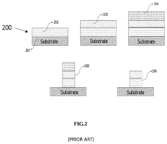
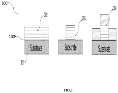
01 Direct integration of SNSPDs on photonic integrated circuits
This approach involves directly fabricating superconducting nanowire single-photon detectors on photonic integrated circuits. The integration process typically includes deposition of superconducting thin films (often niobium nitride or tungsten silicide) directly onto silicon or other photonic waveguide platforms, followed by nanopatterning to create the nanowire structures. This method enables efficient light coupling from waveguides to detectors and minimizes optical losses, resulting in higher detection efficiency and better timing performance.- Direct integration of SNSPDs on photonic integrated circuits: Techniques for directly integrating superconducting nanowire single-photon detectors (SNSPDs) onto photonic integrated circuits (PICs). This approach involves fabricating SNSPDs directly on the same substrate as the photonic waveguides, enabling efficient coupling between the detector and the optical components. The integration process typically includes deposition of superconducting thin films, nanopatterning of the nanowires, and establishing electrical connections while maintaining optical coupling to the waveguides.
- Hybrid integration methods for SNSPDs on PICs: Hybrid integration approaches that combine separately fabricated SNSPDs with photonic integrated circuits. These methods include flip-chip bonding, transfer printing, and pick-and-place techniques to position pre-fabricated SNSPD devices onto PICs. Hybrid integration allows for independent optimization of the superconducting detector and the photonic circuit, overcoming material compatibility challenges while achieving high coupling efficiency between components.
- Waveguide-coupled SNSPD designs: Specialized designs for coupling SNSPDs to optical waveguides in photonic integrated circuits. These designs focus on maximizing the interaction between the evanescent field of the guided optical mode and the superconducting nanowire to achieve high detection efficiency. Various coupling geometries are employed, including U-shaped nanowires wrapped around waveguides, meander patterns on top of waveguides, and tapered waveguide structures to enhance light absorption in the nanowire.
- Cryogenic packaging solutions for integrated SNSPDs: Specialized packaging techniques that enable operation of integrated SNSPDs at cryogenic temperatures while maintaining optical and electrical connections to room-temperature systems. These solutions address thermal isolation, electrical signal integrity, and optical coupling challenges. Approaches include custom cryostat designs with optical windows or fibers, specialized electrical feedthroughs, and thermal management structures to maintain the superconducting state while allowing integration with conventional photonic circuits.
- Materials and fabrication processes for SNSPD-PIC integration: Advanced materials and fabrication processes specifically developed for integrating SNSPDs with photonic integrated circuits. This includes the use of novel superconducting materials compatible with photonic circuit fabrication, such as amorphous superconductors, as well as specialized deposition, etching, and patterning techniques. These processes address challenges related to material compatibility, film quality, and nanoscale patterning required for high-performance integrated single-photon detectors.
02 Hybrid integration techniques for SNSPDs
Hybrid integration involves separately fabricating SNSPDs and photonic integrated circuits, then combining them using various bonding techniques. Methods include flip-chip bonding, transfer printing, and membrane transfer. This approach allows for independent optimization of both the superconducting detector and the photonic circuit, overcoming material compatibility issues. The technique is particularly useful when the optimal fabrication conditions for SNSPDs differ significantly from those for photonic waveguides.Expand Specific Solutions03 Cryogenic packaging solutions for integrated SNSPDs
Specialized cryogenic packaging is essential for SNSPD operation as these devices require extremely low temperatures (typically below 4K). Advanced packaging techniques include development of custom cryogenic housings with efficient thermal interfaces, specialized electrical feedthroughs for signal transmission, and optical fiber coupling mechanisms that maintain alignment during thermal cycling. These packaging solutions address challenges related to thermal contraction, heat load management, and maintaining optical alignment at cryogenic temperatures.Expand Specific Solutions04 Waveguide-coupled SNSPD designs
Specialized waveguide structures are designed to efficiently couple light from photonic integrated circuits to SNSPDs. These designs include evanescent coupling configurations, tapered waveguides, grating couplers, and resonant structures that enhance the interaction between the guided light and the superconducting nanowire. The waveguide geometry is optimized to maximize absorption in the nanowire while maintaining the superconducting properties, resulting in improved detection efficiency and reduced timing jitter.Expand Specific Solutions05 Multi-channel SNSPD arrays on photonic chips
Integration of multiple SNSPD channels on a single photonic chip enables advanced quantum photonic applications requiring coincidence detection or spatial resolution. These designs incorporate multiple nanowire detectors coupled to different waveguide channels, with careful consideration of thermal crosstalk, electrical readout complexity, and uniform performance across channels. Advanced multiplexing schemes and readout electronics are developed to handle the signals from multiple detectors while maintaining the cryogenic temperature requirements.Expand Specific Solutions
Leading Organizations in SNSPD-PIC Integration Research
The integration of Superconducting Nanowire Single Photon Detectors (SNSPDs) on Photonic Integrated Circuits (PICs) is currently in an early growth phase, with significant research momentum but limited commercial deployment. The global market for this technology is expanding, driven by quantum computing and secure communications applications, with projections suggesting substantial growth as quantum technologies mature. Leading academic institutions (MIT, Columbia University, Zhejiang University) are collaborating with specialized companies (PsiQuantum, Single Quantum, Photonic Inc.) to advance technical capabilities. While major challenges remain in cryogenic integration and scalability, recent breakthroughs by Shanghai Institute of Microsystem & Information Technology and ID Quantique demonstrate progress toward practical implementation, with TSMC and IBM exploring manufacturing pathways for larger-scale production.
PsiQuantum Corp.
Technical Solution: PsiQuantum has developed a proprietary integration technique for SNSPDs on silicon photonic platforms specifically optimized for fault-tolerant quantum computing applications. Their approach utilizes molybdenum silicide (MoSi) superconducting nanowires with precisely engineered dimensions (typically 4-6nm thickness) directly integrated with silicon waveguides. PsiQuantum's innovation includes a specialized "traveling-wave" SNSPD design that extends the interaction length between the evanescent field and the superconducting nanowire, achieving detection efficiencies exceeding 95% while maintaining timing jitter below 30ps. Their fabrication process incorporates unique stress-management layers that preserve the superconducting properties of the nanowires during integration with silicon photonics. PsiQuantum has demonstrated large-scale integration with hundreds of SNSPDs on a single chip, connected through sophisticated routing architectures that minimize thermal crosstalk while enabling multiplexed readout schemes.
Strengths: Highly optimized for large-scale quantum computing applications with demonstrated path to thousands of integrated detectors; excellent timing performance enabling high-fidelity quantum operations. Weaknesses: Proprietary process may limit broader adoption; requires ultra-low temperature operation (below 1K) which increases system complexity and operational costs.
Massachusetts Institute of Technology
Technical Solution: MIT has pioneered advanced techniques for integrating Superconducting Nanowire Single-Photon Detectors (SNSPDs) onto photonic integrated circuits (PICs). Their approach utilizes amorphous tungsten silicide (WSi) superconducting nanowires deposited directly onto silicon nitride waveguides, achieving near-unity internal detection efficiency. MIT researchers developed a unique "U-shaped" nanowire geometry that wraps around the waveguide to maximize photon absorption while maintaining superconducting properties. Their integration process includes precise temperature control during deposition (typically below 250°C) to prevent degradation of the superconducting film quality. MIT has also demonstrated successful integration with various photonic circuit components including ring resonators and directional couplers, enabling complex quantum photonic circuits with on-chip detection capabilities.
Strengths: Achieves near-unity internal quantum efficiency with minimal dark count rates; compatible with standard CMOS fabrication processes enabling scalable manufacturing. Weaknesses: Requires sophisticated cryogenic packaging solutions; the amorphous WSi material choice trades higher operating temperature for potentially lower timing performance compared to NbN alternatives.
Key Patents and Breakthroughs in SNSPD-PIC Integration
Superconducting circuit for detecting single photons
PatentWO2025101221A2
Innovation
- The integration of superconducting nanowire single-photon detectors with Josephson electronics and CMOS readout architectures, allowing for local signal integration at each pixel and decoupling detection events from the readout process, thereby enabling scalable and efficient detection of single photons.


Method and systems for fabricating superconducting nanowire single photon detector (SNSPD)
PatentPendingUS20230031577A1
Innovation
- A method and system for fabricating superconducting nanowire single photon detectors using high temperature superconductors with pulsed laser deposition, eliminating post-processing of superconducting thin films and gold encapsulation to maintain material quality and enable operation above 4 K.
Cryogenic Packaging Solutions for Integrated SNSPD Devices
The integration of Superconducting Nanowire Single-Photon Detectors (SNSPDs) with Photonic Integrated Circuits (PICs) presents significant challenges in terms of packaging, primarily due to the cryogenic operating requirements of SNSPDs. Conventional packaging solutions designed for room temperature operation are inadequate for maintaining the necessary sub-Kelvin temperatures required for optimal SNSPD performance.
Current cryogenic packaging solutions employ various approaches to address thermal management challenges. Closed-cycle refrigeration systems, including pulse tube coolers and Gifford-McMahon refrigerators, have emerged as preferred options for laboratory and field deployments, offering temperatures down to 2-4K without liquid cryogens. For applications requiring sub-Kelvin temperatures, adiabatic demagnetization refrigerators (ADRs) and dilution refrigerators provide additional cooling stages.
Thermal isolation represents a critical aspect of cryogenic packaging design. Advanced solutions utilize vacuum-insulated chambers with radiation shields to minimize heat transfer through conduction, convection, and radiation. Materials selection plays a pivotal role, with low thermal conductivity materials like aerogels, multi-layer insulation (MLI), and specialized polymers being employed for structural components.
Electrical interconnects present another significant challenge, as conventional wiring introduces thermal loads. Superconducting wires offer minimal thermal conductivity while maintaining zero electrical resistance, though they require careful design to prevent quenching. High-density electrical feedthroughs with minimal thermal conductance have been developed specifically for cryogenic applications.
Optical coupling solutions have evolved to accommodate the extreme temperature differentials. Fiber-to-chip coupling techniques using specialized fiber arrays with thermal compensation mechanisms help maintain alignment across temperature gradients. Alternatively, free-space coupling approaches utilizing cryostat windows with anti-reflection coatings provide another viable solution, though with increased complexity.
Recent innovations include monolithic integration approaches where SNSPDs are directly fabricated on PIC platforms, significantly reducing packaging complexity. This approach requires compatible material systems and careful process development but offers superior optical coupling efficiency and system miniaturization.
Modular cryogenic packaging platforms have emerged as a promising direction, offering standardized interfaces for both electrical and optical connections. These platforms facilitate rapid prototyping and testing of integrated SNSPD-PIC systems while maintaining the necessary cryogenic environment. Commercial solutions from companies like Montana Instruments, Janis Research, and Oxford Instruments provide turnkey systems with customizable options for research and early commercial applications.
Scalability remains a significant challenge for cryogenic packaging solutions. Current approaches typically accommodate small numbers of devices, but emerging applications in quantum computing and communications demand arrays of hundreds or thousands of integrated SNSPDs. Advanced multiplexing schemes and three-dimensional integration techniques are being explored to address these scaling challenges.
Quantum Computing Applications and Ecosystem Impact
The integration of Superconducting Nanowire Single-Photon Detectors (SNSPDs) on Photonic Integrated Circuits (PICs) represents a transformative advancement for quantum computing applications. This technology enables unprecedented detection efficiency and timing resolution, serving as a critical enabler for quantum information processing, quantum key distribution, and quantum networking.
Quantum computing stands to benefit significantly from integrated SNSPD-PIC platforms. These systems facilitate the precise manipulation and measurement of quantum states necessary for quantum algorithms that can solve complex problems intractable for classical computers. Applications such as Shor's algorithm for factoring large numbers and Grover's search algorithm become more practically implementable with reliable single-photon detection integrated directly into quantum processing units.
The ecosystem impact extends beyond computational advantages. Financial institutions are exploring quantum-resistant cryptography solutions that rely on quantum key distribution systems, where integrated SNSPDs provide the necessary security guarantees. The pharmaceutical industry stands to benefit from quantum simulations of molecular structures, potentially revolutionizing drug discovery processes through more accurate modeling of quantum mechanical interactions.
Material science research will experience acceleration through quantum simulations enabled by these integrated photonic platforms. The ability to model complex quantum systems could lead to the discovery of novel materials with properties optimized for energy storage, superconductivity, or structural applications. This represents a significant economic opportunity, with potential market value estimated in the billions.
The emergence of quantum networks—connecting quantum computers across geographic distances—depends critically on reliable single-photon detection. SNSPD-PIC integration provides the foundation for quantum repeaters and quantum memory interfaces necessary for such networks. This infrastructure could eventually support a quantum internet, enabling distributed quantum computing and secure communications on a global scale.
Supply chains for quantum technologies are evolving rapidly, with specialized fabrication facilities developing capabilities for superconducting device integration with photonic circuits. This ecosystem development is creating new job categories and educational requirements, driving universities to establish quantum engineering programs to meet workforce demands.
Government and private investment in quantum technologies continues to grow, with major initiatives in the US, Europe, China, and Japan. The strategic importance of quantum capabilities is driving national policies aimed at securing technological sovereignty in this domain, further accelerating ecosystem development around integrated quantum photonic technologies.
Unlock deeper insights with PatSnap Eureka Quick Research — get a full tech report to explore trends and direct your research. Try now!
Generate Your Research Report Instantly with AI Agent
Supercharge your innovation with PatSnap Eureka AI Agent Platform!