
A dual-mode ellipse response filter of substrate integration waveguide
A substrate-integrated waveguide and filter technology, applied to waveguide devices, connecting devices, electrical components, etc., can solve the problems of complex design and difficult implementation, and achieve the effects of simple design, convenient grounding and isolation, and high precision
- Summary
- Abstract
- Description
- Claims
- Application Information
AI Technical Summary
Problems solved by technology
Method used
Image

Examples
Embodiment Construction
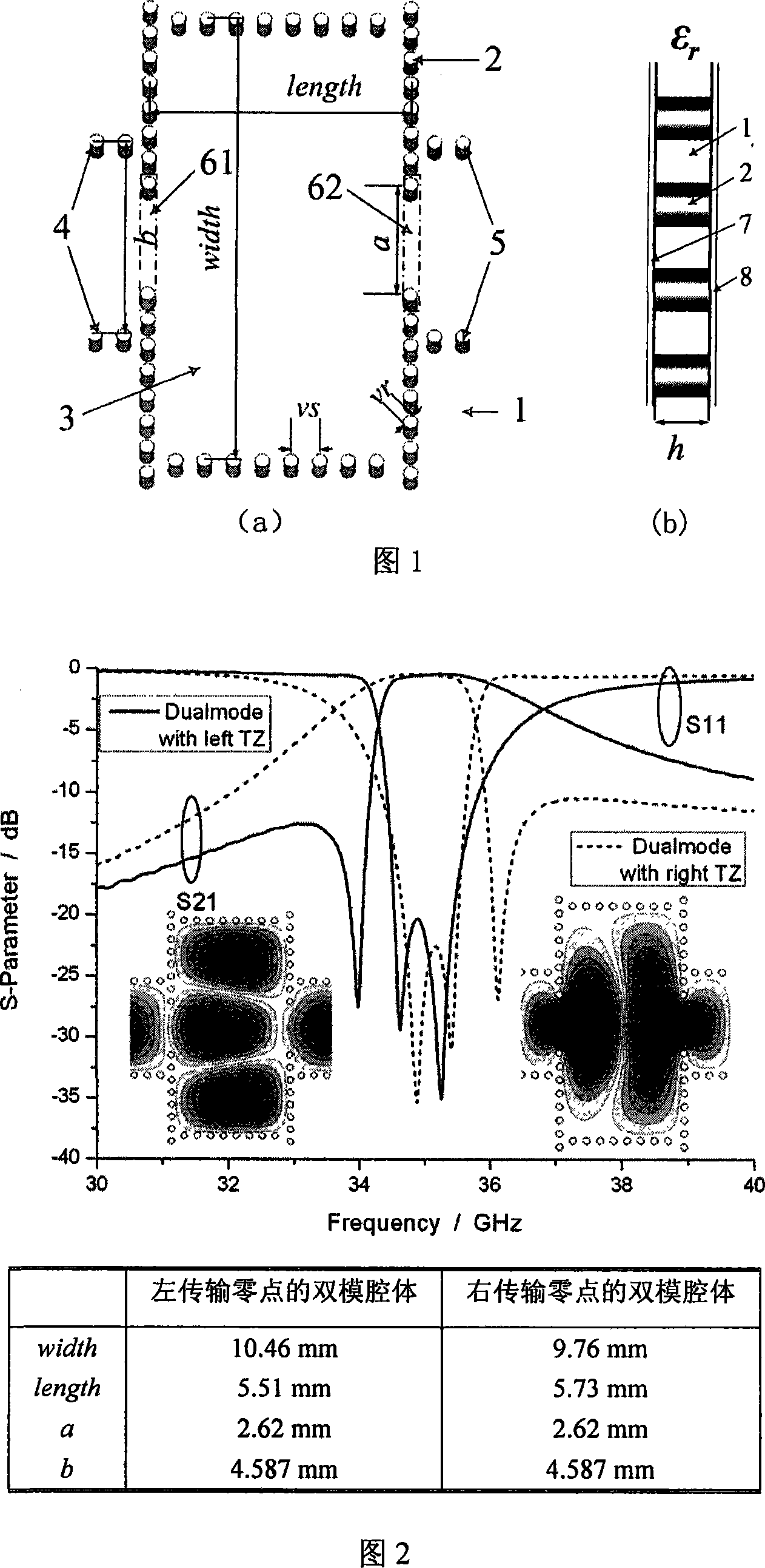
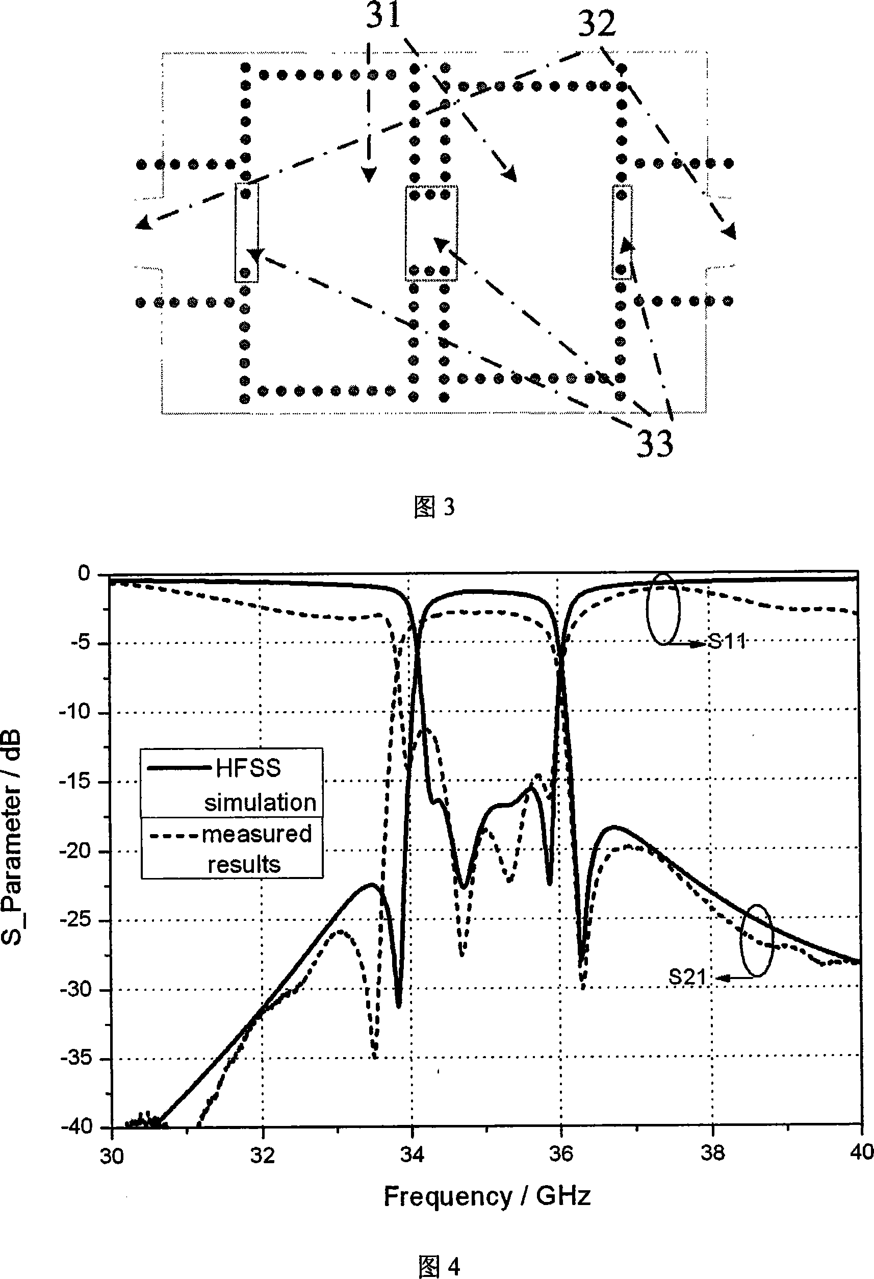
[0021] The dual-mode cavity elliptic response filter uses two dual-mode single cavities with different sizes to obtain an elliptic response with bilateral steep drops, and each single cavity contributes one zero point and two poles. The structure of the single cavity is shown in Figure 1. It adopts the substrate integrated waveguide technology, including the dielectric substrate 1, the upper surface metal layer 7 and the lower surface metal layer 8 coated on the upper and lower surfaces of the dielectric substrate 1, and the The metallized through-hole array 2 of the upper surface metal layer 7 and the lower surface metal layer 8 of the upper and lower metal surfaces. The cavity 3 with a rectangular structure is a standard rectangular structure, and the first inductive coupling hole 61 and the second inductive coupling hole 62 lead energy into and out of the cavity. The first metallized through-hole array 4 and the second metallized through-hole array 5 correspond to the input...
PUM
| Property | Measurement | Unit |
|---|---|---|
| Width | aaaaa | aaaaa |
| Width | aaaaa | aaaaa |
| Diameter | aaaaa | aaaaa |
Abstract
Description
Claims
Application Information