
Detection of low-frequency signal processing chip and low-frequency signal processing circuit
A technology for processing chips and low-frequency signals. It is applied in the direction of adjusting electrical variables, control/regulating systems, instruments, etc., and can solve problems such as false triggering and low-frequency fluctuations in power supply voltages that cannot be effectively suppressed.
Patent Information
- Authority / Receiving Office
- CN · China
- Patent Type
- Applications(China)
- Current Assignee / Owner
- Publication Date
- 2018-10-19
Smart Images
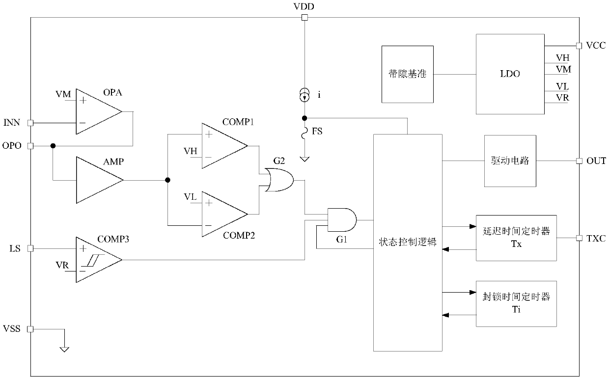
Figure 1 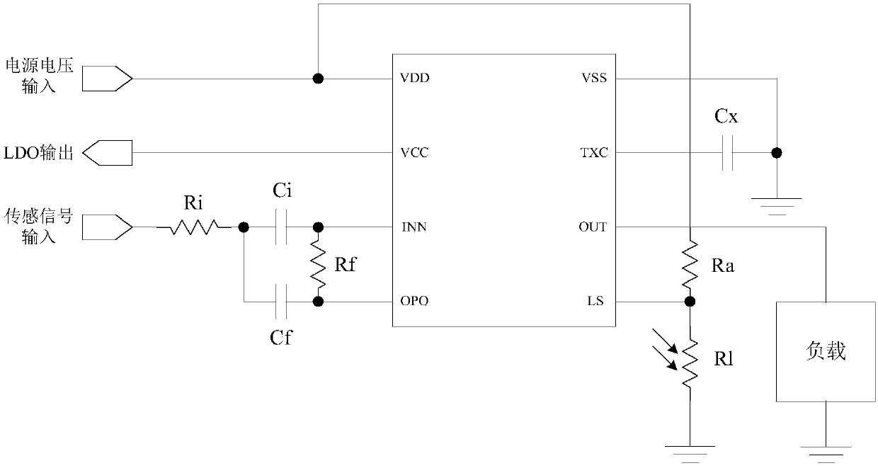
Figure 2 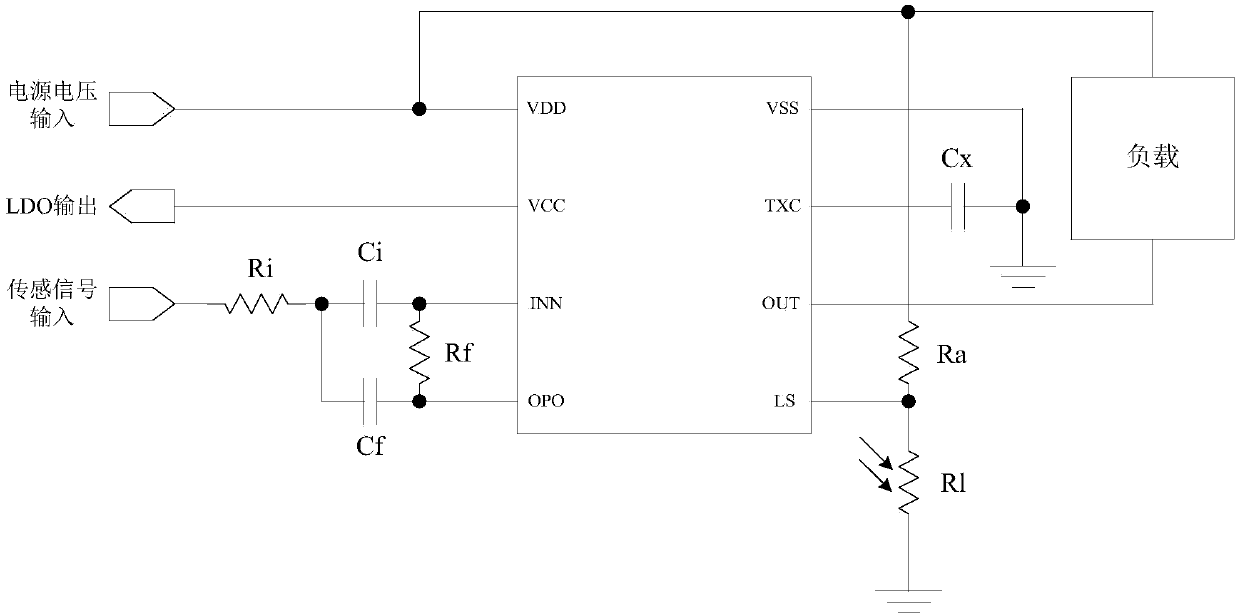
Figure 3
Abstract
Description
technical field
[0001] The invention belongs to the field of integrated circuits, and in particular relates to a detecting low-frequency signal processing chip and a low-frequency signal processing circuit. Background technique
[0002] The early human body sensing chips had many pins and low integration, and more components such as resistors and capacitors were needed around the chip to cooperate with the chip to realize signal processing and control functions.
[0003] In recent years, more integrated human body sensing chips have appeared on the market, with simple peripheral circuits and fewer components. This type of chip retains the second-stage band-pass amplifier of the early chip circuit system as the first-stage amplifier, while the second stage amplifier is fully integrated into the chip. Since the frequency of human body motion signals is very low, generally 0.3Hz to 3Hz, the peripheral capacitors required by the bandpass filter are usually large-capacity electr...
Examples
Embodiment Construction
[0072] To achieve the above object, the technical solution of the present invention is as follows.
[0073] see figure 1 As shown, the present invention provides a detection low-frequency signal processing chip, the processing chip includes VDD pins, VCC pins, OUT pins, TXC pins, VSS pins, LS pins, OPO pins and INN pins ; VDD is electrically connected to the state control logic circuit through the current source, and one end of the fuse FS is electrically connected between the current source i and the state control logic circuit, and the other end of the fuse FS is grounded; the VCC pin passes through a low-dropout linear regulator The LDO (low dropout regulator) circuit is electrically connected to the high-precision bandgap reference circuit; the OUT pin is electrically connected to the state control logic circuit through the drive circuit; the TXC pin is electrically connected to the state control logic circuit through the delay time timer Tx; the state The control logic c...