
Semiconductor device having a molded package
a semiconductor device and package technology, applied in semiconductor devices, semiconductor/solid-state device details, electrical apparatus, etc., can solve the problems of low heat dissipation effect, inability and difficulty in performing electrical grounding and heat dissipation separately from each other, so as to improve high-frequency characteristics and improve heat dissipation effect.
- Summary
- Abstract
- Description
- Claims
- Application Information
AI Technical Summary
Benefits of technology
Problems solved by technology
Method used
Image

Examples
first embodiment
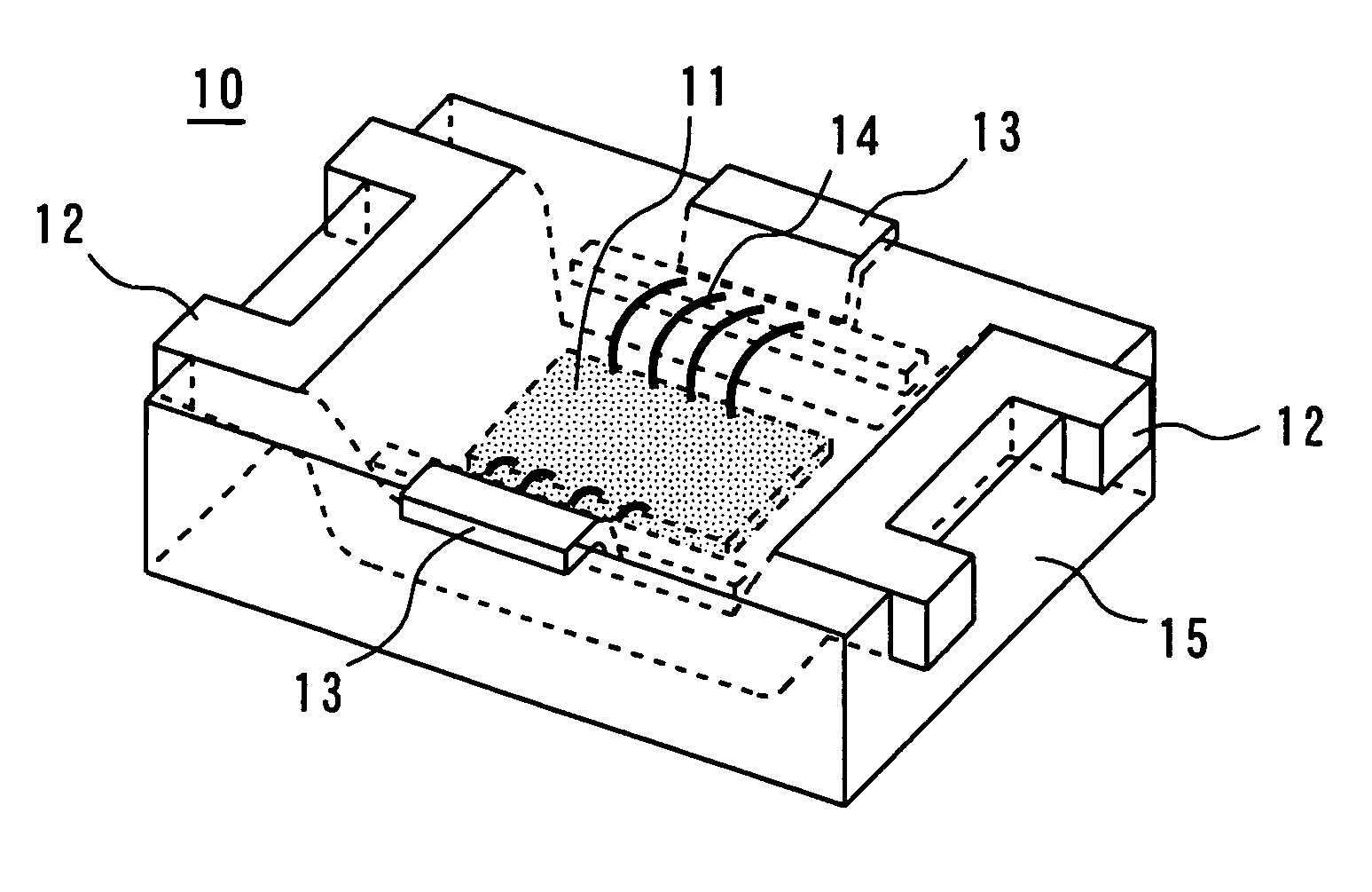
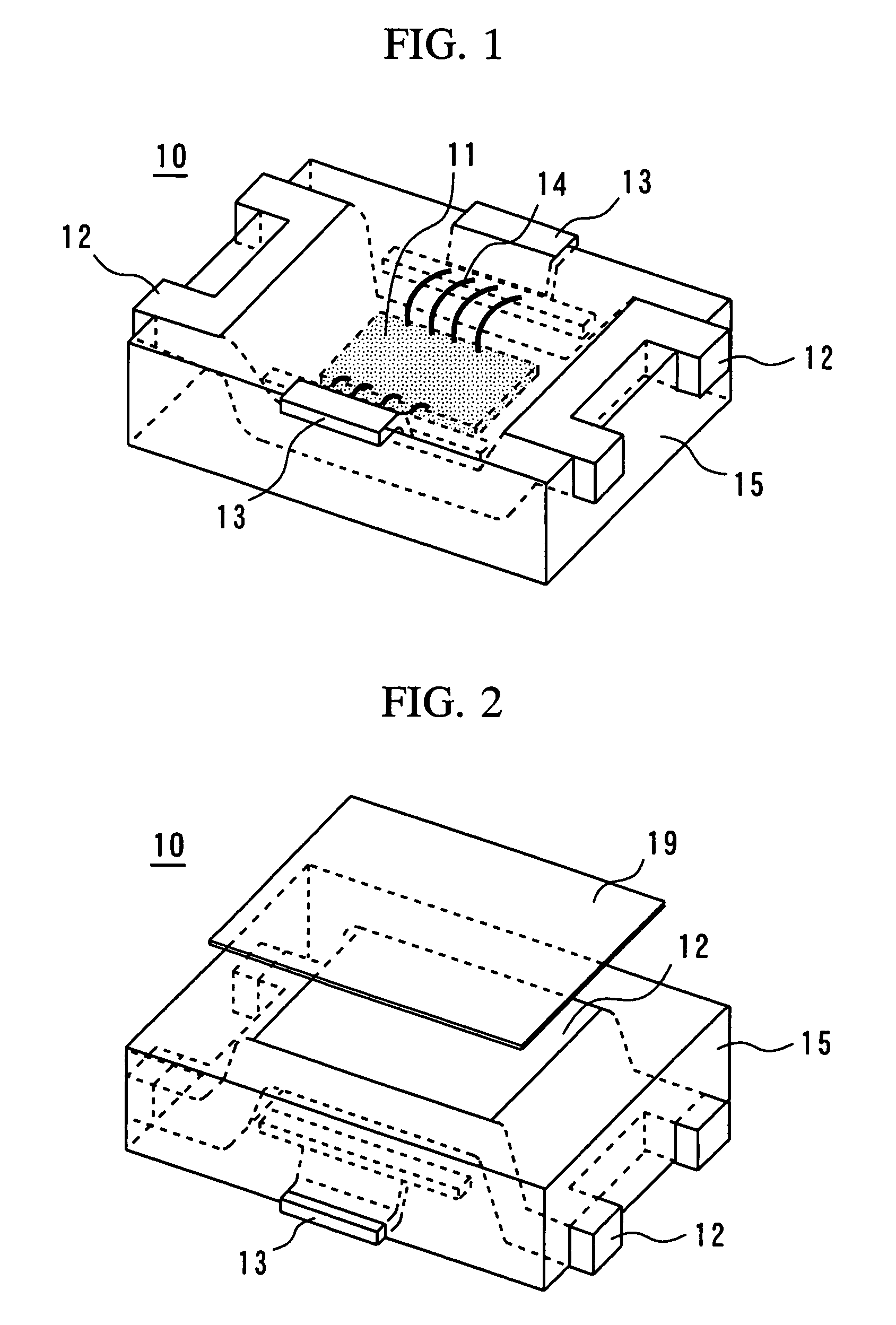
[0030]FIG. 1 is a perspective view showing a molded package according to a first embodiment of the present invention. FIG. 2 shows a state in which the molded package shown in FIG. 1 is placed upside down. As illustrated, a semiconductor chip 11 is die-bonded, for example, by soldering to a recessed portion of a thick-film lead electrode 12 having a thickness of about 0.4 to 1.0 mm. The recessed portion is formed by bending the thick-film lead electrode 12 on opposite sides of a central portion of the thick-film lead electrode 12. Thin-film lead electrodes 13 having a thickness of about 0.05 to 0.2 mm are bent downward so as to be closer to the semiconductor chip 11 and are electrically connected to the semiconductor chip by metal wires 14. The semiconductor chip 11 and the metal wires 14 are encapsulated in a molding material 15 such as a plastic to form a molded package 10.
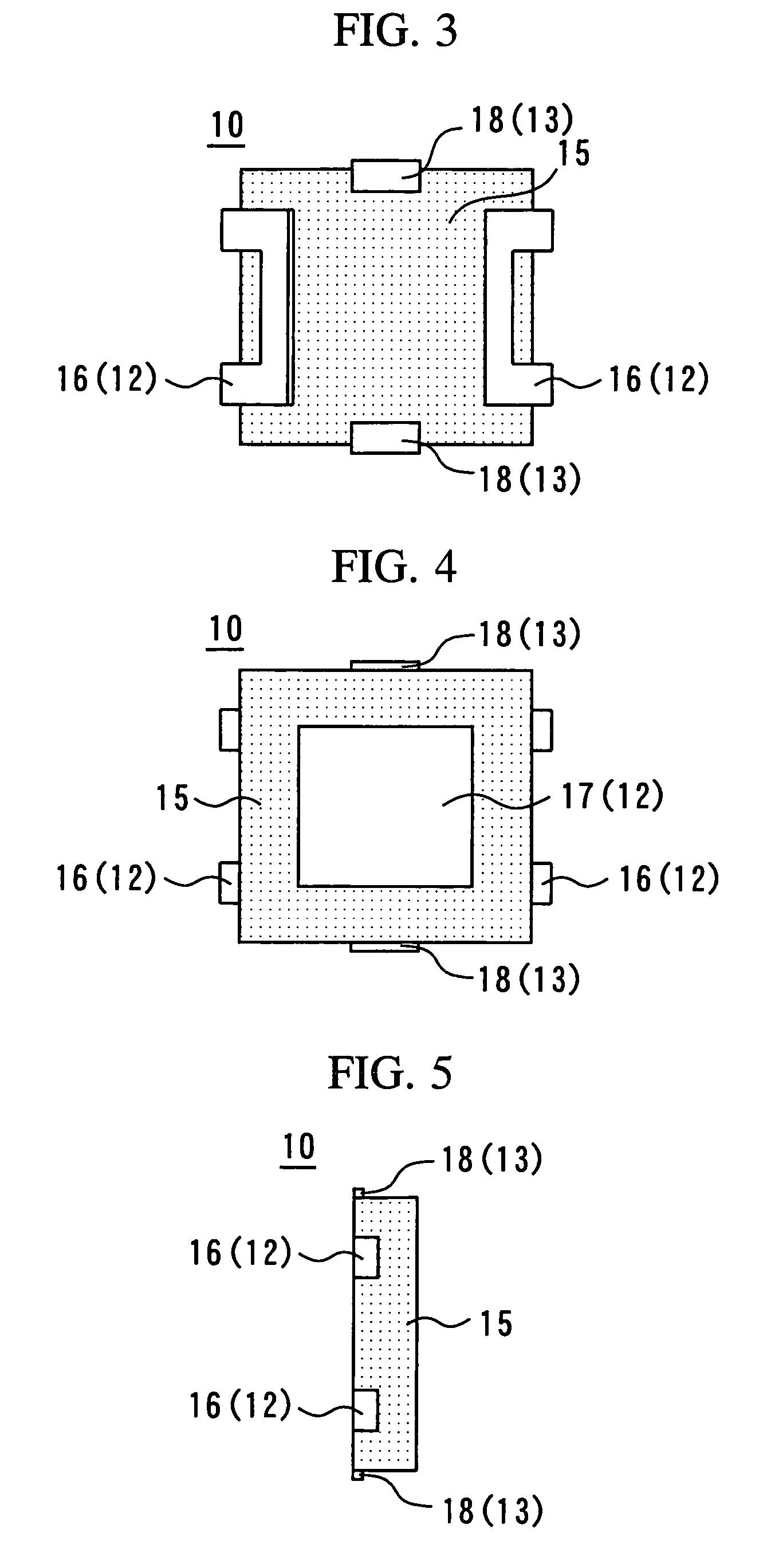
[0031]FIG. 3 shows a top view of this molded package; FIG. 4 a bottom view; and FIG. 5 a side view. As illust...
second embodiment
[0044]FIG. 11 is a sectional view showing a molded package according to a second embodiment of the present invention. Constituents identical or corresponding to those shown in FIGS. 1 through 10 are indicated by the same reference numerals and the description for them will not be made.
[0045]In the molded package according to this embodiment, a copper oxide film 27 is precipitated on a plating layer 24 formed by plating with silver (Ag) for example. The closeness of contact between the thick-film lead electrode 21 and the molding material 15 in the vicinity of the semiconductor chip 11 is thereby improved to further improve the reliability of the semiconductor chip 11.
[0046]As a method for precipitation of the copper oxide film 27 on the plating layer 24, a method may be used in which the surface of the thick-film lead electrode 21 is oxidized in an atmosphere in which the proportion of an inert gas such as nitrogen (N2) is high to cause copper oxide formed on the surface of the thic...
PUM
 Abstract
Description
Claims
Application Information