
Junction field effect transistor
A field effect transistor and junction gate technology, which is applied in the field of microelectronic semiconductors, can solve the problem of device size gate oxide, the thermal electron effect cannot be effectively solved, etc., and is suitable for large-scale integration, cost saving, and good heat dissipation efficiency. Effect
Patent Information
- Authority / Receiving Office
- CN · China
- Patent Type
- Patents(China)
- Current Assignee / Owner
- Publication Date
- 2008-06-25
- Estimated Expiration
- Not applicable · inactive patent
Smart Images
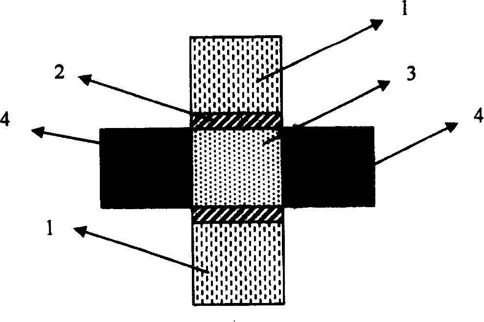
Figure 1 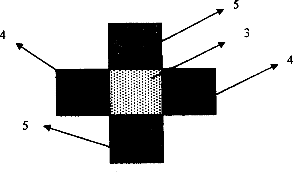
Figure 2 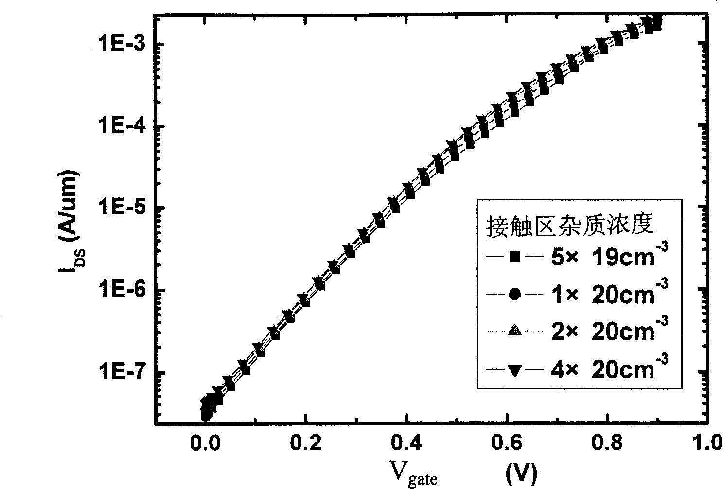
Figure 3
Abstract
Description
technical field
[0001] The invention belongs to the technical field of microelectronics and semiconductors, and in particular relates to a double gate junction gate field effect transistor. Background technique
[0002] With the continuous development of microelectronics technology, the density of circuit integration is increasing, the size of devices is becoming smaller and smaller, and the difficulty of integration is also increasing. Especially after decades of rapid development, the size of microelectronic devices has entered the nanoscale. Many effects that only appear in small sizes seriously threaten the development of devices, and then affect the progress of the entire microelectronics technology. For example, with the continuous shrinking of the device size, the preparation of high-quality thin-layer gate oxide is an insurmountable difficulty in the current process. Although there are many alternative technologies, such as high-K dielectric (Oates et al., IEDM Tec...
Examples
Embodiment Construction
[0020] Specific implementation examples
[0021] refer to figure 2 , the dual gate junction gate field effect transistor of the present invention comprises: source region 4, drain region 4, double control gate 5 and body 3, body 3 is square, control gate 5 is doped monocrystalline silicon, control gate and body are directly connected Form a P-N junction, the body is a square. It can be seen from the figure that the dual-gate junction gate field effect transistor of the present invention is a completely symmetrical structure, so as long as the connecting electrodes between the control gate and the source and drain are changed, the n-type double gate junction gate field effect transistor and the p-type double gate field effect transistor.
[0022] The specific implementation example of the double-gate junction gate field effect transistor of the present invention, taking the side length of the body as an example, its specific design structural parameters are as follows: the l...