
Flat resolution correcting method for image optical system and apparatus thereof
A technology of planar resolution and optical system, which is applied in the parts of TV system, image communication, TV, etc., can solve the problems affecting the accuracy and speed of correction, linear error, and the increase of the complexity of optical system mechanism, etc.
Patent Information
- Authority / Receiving Office
- CN · China
- Patent Type
- Patents(China)
- Current Assignee / Owner
- Publication Date
- 2009-10-21
- Estimated Expiration
- Not applicable · inactive patent
Smart Images
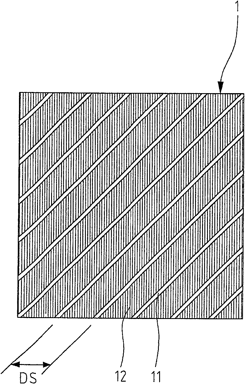
Figure 1 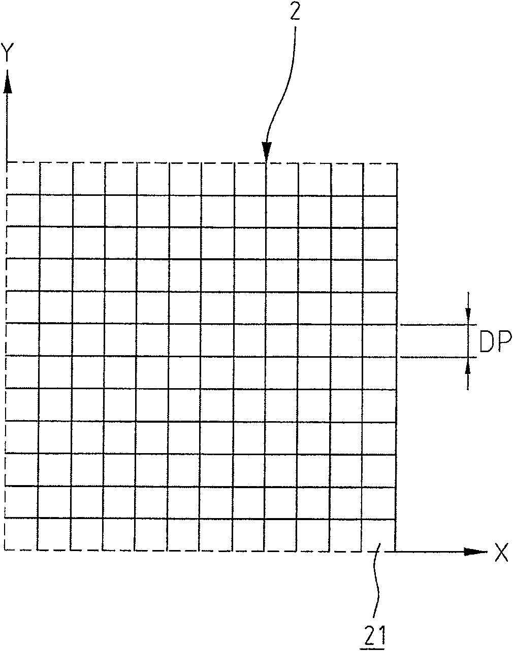
Figure 2 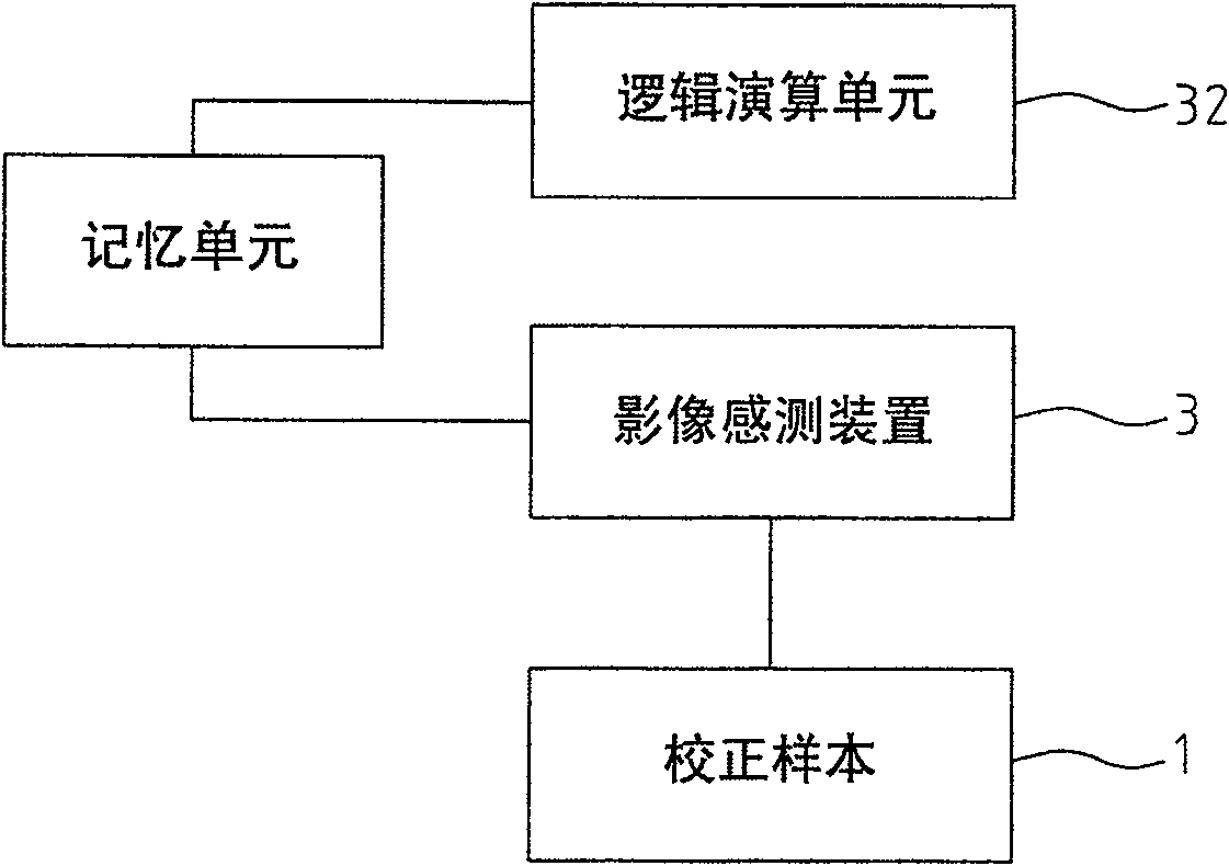
Figure 3
Abstract
Description
technical field
[0001] The present invention relates to a plane resolution calibration method of an image optical system and its device, and in particular provides a calibration method for an image capture device, which is used to correct the image magnification corresponding to the pixels. Background technique
[0002] The known planar resolution calibration method of an image optical system provides calibration for an image capture device to determine the image magnification corresponding to the pixels of a CCD sensor or a CMOS sensor. Usually this kind of technology is to capture the image of the scale scale marked with the size through the image capture device, refer to Figure 7 As shown, the two scale line positions P1 and P2 are selected by image processing or manually, and the pixel distance between them is calculated, and the actual distance between P1 and P2 on the scale 6 is determined by design. By comparing the actual distance size with the pixel distance, the a...
Examples
Embodiment Construction
[0029] figure 1 It is a schematic diagram showing the calibration samples used in the plane resolution calibration method of the imaging optical system of the present invention; figure 2 It is a schematic diagram showing the coordinates of the sensing component of the method for correcting the planar resolution of the image optical system of the present invention. refer to figure 1 As shown, it is the calibration sample 1 used in the present invention. The calibration sample 1 has several bright lines 11 and dark lines 12 alternate stripes, and the bright lines 11 are parallel to each other and have the same width, and the dark lines 12 are also parallel to each other. and have the same width, wherein the actual distance between the bright lines 11 is denoted as DS. Also, refer to figure 2 As shown, it is a schematic diagram of the measurement coordinates 2 not shown in the figure of the image sensing device used in the present invention, wherein each unit cell 21 corre...